
Additive Multiply Module Architecture for Low Power 8-Bit
Multipliers in VLSI
Vasudeva G
1
, Gopal Chandra Sarkar
2
, Aniket Magadum
1
, Mohammed Asif
1
, Adarsh Khot
1
,
and B H M Siddesh
1
1
Department of ECE, Dayananda Sagar Academy of Technology and Management, Bangalore, Karnataka, India
2
Department of EEE, Dayananda Sagar Academy of Technology and Management, Bangalore, Karnataka, India
Keywords: Additive Multiply Module, Low-Power
VLSI, 8-Bit Multiplier, Power Optimization, Xilinx ISE, Cadence
EDA, AMM, Dadda and Wallace Tree.
Abstract: Multipliers are fundamental in digital signal processing and VLSI systems, directly affecting power, area, and
speed. This paper presents the design and FPGA implementation of an 8-bit multiplier using Additive
Multiply Module (AMM) architecture aimed at low-power, high-efficiency applications. The proposed
AMM-based design is developed and verified on an FPGA and its experimental performance is benchmarked
against conventional Wallace Tree and Dadda multipliers. Results confirm that the AMM multiplier not only
reduces power consumption—but also achieves competitive area and delay—making it well-suited for modern
embedded and IoT VLSI design environments.
1
INTRODUCTION
Multiplication is a key arithmetic function in many
VLSI applications, particularly those involving digital
signal processing and embedded computation. The
energy efficiency of these systems largely depends on
the performance and design of hardware multipliers.
(Parameshwara, M C 2021. Conventional multiplier
architectures such as Wallace Tree and Dadda
prioritize speed but often result in increased power
consumption and area (Choppala, P., Gullipalli et al.,
2021). With the advent of portable and IoT devices,
there is a pressing need formultiplier designs that
balance speed, power, and silicon area (Jain, A.,
Bansal et al., 2019).
This research introduces and implements an 8- bit
Additive Multiply Module (AMM) architecture
(Munawar, M., Shinde et al., 2019), focusing on
reducing dynamic power and hardware complexity
while maintaining computation speed. The work
provides a practical evaluation of the AMM approach
(Parameshwara, M. C., et al., 2019) by synthesizing
and benchmarking its performance on FPGA
hardware and comparing it with Wallace Tree and
Dadda multipliers (Tung, C. W et al.,2019; Seo, Y.-
H. et al., 2020).
2
LITERATURE SURVEY
Power and area-efficient multiplier design is a long-
standing research focus in VLSI and digital signal
processing(Marimuthu, C. N etal., 2018), as
multipliers are critical for performance and energy
consumption in embedded and portable
systems(Chen, K. H et al., 2006). Several
architectural innovations and methodologies have
shaped the current landscape for low- power
multipliers*( Lakshmi Narayanan, G et al., 2022).
(Chen, K. H et al., 2022). proposed approximate
full adder (FA) architectures with reduced switching
activity, specifically targeting image processing and
multimedia workloads. Their work demonstrated that
by enabling controlled errors in adder outputs for least
significant bits, significant reductions in energy
consumption could be achieved without perceptible
loss in output quality in error-resilient applications
(Zicari, P et al.,2005). Similarly, reversible logic-
based FAs were investigated for quantum cost
reductions and minimum garbage output Huang, Z et
al., 2024), indicating promise for ultra-low power
digital signal processors Lee, H. (2024).
(Fayed, A., et al 2022). introduced a Gate
Diffusion Input (GDI) based 1-bit hybrid FA,
192
G, V., Sarkar, G. C., Magadum, A., Asif, M., Khot, A. and Siddesh, B. H. M.
Additive Multiply Module Architecture for Low Power 8-Bit Multipliers in VLSI.
DOI: 10.5220/0014379900004848
Paper published under CC license (CC BY-NC-ND 4.0)
In Proceedings of the 2nd International Conference on Advances in Electrical, Electronics, Energy, and Computer Sciences (ICEEECS 2025), pages 192-197
ISBN: 978-989-758-783-2
Proceedings Copyright © 2026 by SCITEPRESS – Science and Technology Publications, Lda.

containing only 14 transistors, and embedded it within
both array and Wallace Tree multipliers(Choi, J.,
Jeon, J., & Choi, K. (2000). The result was a notable
reduction in both silicon area and dynamic power,
while the use of hybrid full adders assisted in
recovering voltage swing lost by prior GDI-only
designs. Hybrid implementations were found to
address some shortcomings of pure-CMOS and pure-
GDI multipliers, and simulation under 250nm
technology showed substantial improvements over
traditional designs (Benini, L et al., 2020). Wallace
Tree-based multipliers specifically benefited from
this arrangement, achieving low area and high-speed
operation for larger bit-widths compared to classical
structures (Elguibaly, F. 2020).
Jain et al. built on this by integrating Vedic
mathematics with Booth and Wallace Tree
algorithms, culminating in hybrid multiplier designs
that exploit the advantages of each approach. Their
Radix-4 Booth and Wallace algorithm fusion led to
reductions in both critical path delay and area. The
resulting architecture suits applications where both
computational speed and hardware optimization are
necessary. Similar combinations of high- speed
arithmetic techniques reflect the industry's direction
toward multipliers tailored to diverse, domain-
specific requirements.
Munawar et al. modified Dadda multipliers with
carry select adders and binary to excess-1 converters,
which delivered additional speed improvements and
power reductions over traditional Dadda Tree and
array multipliers (Fadavi-Ardekani, J. 2022). Their
Cadence-based analysis using 180nm technology
highlighted that judicious adder selection and
architectural modularity can further balance energy,
timing, and layout requirements for custom VLSI
accelerators (Cooper, A. R. 1988).
Finally, Tung and Huang proposed a high-
performance, pipelined multiply-accumulate (MAC)
unit that integrates additions and accumulations
directly into the partial product reduction process,
thus minimizing the delays and switching activity of
conventional accumulation strategies. This approach
is especially beneficial in applications requiring
repeated MAC operations, such as DSP and neural
network inference engines.
In summary, recent literature reflects a strong
progression from conventional, speed-oriented
multiplier architectures (e.g., Wallace, Dadda, Braun)
toward designs that optimize for energy efficiency and
silicon area, often at the architectural, logic, and even
transistor level. Architectural segmentation, selective
approximation, reversible logic, and hybrid CMOS-
GDI implementations are central to these
advancements. The Additive Multiply Module
(AMM) multiplier is developed in this context,
employing operand segmentation and efficient adder
arrangements to capitalize on these trends, making it
highly suitable for modern low-power VLSI systems
where trade- offs between accuracy, power, and area
are key design considerations.
3
METHODOLOGY
3.1 Input Division Strategy
The multiplicand and multiplier are systematically
divided into smaller segments to facilitate partial
product generation, .Multiplicand Division, The 8-bit
multiplicand, denoted as A, is partitioned into two 4-
bit segments: a higher-order part (AH) and a lower-
order part (AL). This division can be mathematically
expressed as:
A=(AH×24)+AL or A=(AH≪4)+AL (1)
where AH represents the most significant 4 bits and
AL represents the least significant 4 bits of A. For
instance, if A=(a7a6a5a4a3a2a1a0), then
AH=(a7a6a5a4) and AL=(a3 a2a1a0), The 8-bit
multiplier, denoted as B, is divided into four 2-bit
segments, ordered from most significant to least
significant: B3,B2,B1,B0. This decomposition can be
represented as[1]:
B=(B3×26)+(B2×24)+(B1×22)+B0 (2)
or, equivalently, using bitwise left shifts:
B=(B3≪6)+(B2≪4)+(B1≪2)+B0 (3)
Here, B3,B2,B1,B0 are individual 2-bit groups. For
example, if B=(b7b6b5b4b3b2b1b0)2, then
B3=(b7b6)2, B2=(b5b4)2, B1=(b3b2)2, and
B0=(b1b0)2.
This division strategy enables the generation of
smaller, less complex partial products, which are
fundamental to the efficient design of the overall
multiplier architecture.
3.2 Bitwise Partial Product Generation
Following the systematic segmentation of the 8-bit
multiplicand A and multiplier B as described in
Section II- A, the next critical step involves the parallel
generation of partial products. This phase leverages
the inherent bitwise nature of digital multiplication to
decompose the overall operation into simpler, smaller-
Additive Multiply Module Architecture for Low Power 8-Bit Multipliers in VLSI
193

scale computations.
Operational Mechanism: Each 2-bit segment of
the multiplier, denoted as Bi∈{B0,B1,B2,B3}, is
multiplied with each 4-bit segment of the
multiplicand, Aj∈{AL,AH}. This "multiplication" at
the hardware level is fundamentally realized through
a series of bitwise AND operations. For a general
case, if we consider a 4-bit multiplicand
X=(x3x2x1x0) and a 2- bit multiplier Y=(y1 y0), the
product P=X×Y is formed by:
P=(X AND y0)≪0+(X AND y1)≪1 (4)
This illustrates that the operation is a combination of
AND gates for partial bit products and subsequent bit
shifting for proper positional weighting, followed by
accumulation.
Total Partial Products Derived: Given that the
multiplicand is divided into two parts (AH,AL) and
the multiplier into four parts (B0,B1,B2,B3), the total
number of primary partial products (PPx,y) generated
is 2×4=8. These partial products constitute the
foundational elements that will be subsequently
shifted and summed to form the final 16-bit product.
Enumeration of Generated Partial Products: The
eight distinct partial products are formally defined as
follows:
PPH0=AH×B0 (5)
PPH1=AH×B1 (6)
PPH2=AH×B2 (7)
PPH3=AH×B3 (8)
PPL0=AL×B0 (9)
PPL1=AL×B1 (10)
PPL2=AL×B2 (11)
PPL3=AL×B3 (12)
Each of these individual partial products is the result
of a 4-bit by 2-bit multiplication. The maximum width
of each partial product will be 4+2=6 bits. For
instance, the maximum value of a 4-bit number is 15
(11112) and a 2- bit number is 3 (112). Their product,
15×3=45, requires ⌈log2(45)⌉=6 bits to represent
(1011012). This phase is implemented using an array
of smaller, optimized multiplier blocks, significantly
reducing the gate count and critical path delay
compared to a monolithic 8-bit multiplier[1][2].
This systematic approach significantly reduces
switching activity and complexity, leading to
decreased area and lower power consumption
compared to classical Wallace and Dadda
architectures while maintaining accuracy and
throughput.
3.3 Partial Product Alignment and
Accumulation
Upon the generation of the eight individual partial
products (PPs) as described in Section II-B, the
subsequent critical phases involve their proper
alignment and efficient accumulation to synthesize
the final 16-bit product.
Partial Product Alignment: The bitwise
multiplication step yields 8 partial products, each of
6-bit width (PPH0,…,PPL3). These intermediate
results must be precisely aligned according to the
positional weight of the multiplier segments from
which they were derived. This alignment is crucial for
accurate summation. Considering the original
multiplier B=[B3,B2,B1,B0], where Bi is a 2-bit
segment representing bits (2i+1,2i), the partial
products generated from Bi must be left-shifted by 2i
positions relative to the least significant bit (LSB) of
the overall product. Similarly, partial products
derived from AH are inherently shifted by 4 bits
compared to those from AL. For instance, the partial
product PPH3=AH×B3 would be the most significant
term, requiring a significant left shift due to AH's
position (4 bits) and B3's position (6 bits).
Specifically, PPH3 corresponds to the term
(AH×24)×(B3×26)=AHB3×210. Each partial
product PPXY contributes to the final product P
as[1][2][3]:
P=x∈{H,L}∑y∈{0,1,2,3}∑(PPxy≪shiftxy) (13)
where shift xy is the appropriate bit shift based on the
segment positions. This process effectively converts
the products of segments into terms that can be
summed to form the final product.
Accumulation Strategy: The final 16-bit product of
the 8- bit multiplicand A and 8-bit multiplier B is
obtained by summing these 8 carefully aligned partial
products. This accumulation process is fundamental to
all binary multipliers.
As an illustrative example, consider
A=101011002 and B=111001102. After dividing the
inputs into AH,AL and B3,B2,B1,B0, the partial
products PPxy would be computed. These PPxy
values are then appropriately shifted and added
together. The overall multiplication P=A×B can be
conceptually expanded as:
A×B=((AH≪4)+AL)×((B3≪6)+(B2≪4)+(B1≪2)+B
0)
(14)
Expanding this expression reveals numerous terms,
each corresponding to a shifted partial product PPxy,
ICEEECS 2025 - International Conference on Advances in Electrical, Electronics, Energy, and Computer Sciences
194
necessitating a robust adder architecture for their
summation.
3.4
Final Product Generation
The culmination of the partial product generation and
accumulation stages is the derivation of the final 16-
bit product. This output represents the accurate result
of multiplying the original 8-bit multiplicand A by the
8- bit multiplier B.
The rationale for a 16-bit output is rooted in the
fundamental properties of binary multiplication.
When two N-bit numbers are multiplied, the
maximum possible product can require up to 2N bits
for its representation. In this specific case, multiplying
two 8- bit numbers (where N=8) yields a maximum
product of 28×28=216. Therefore, a 16-bit register is
necessary and sufficient to precisely store the
complete range of possible results, from 0×0=0 to
255×255=65,025. This ensures no overflow or loss of
precision.[2][5]
The final 16-bit output effectively synthesizes all
the contributions from the decomposed higher and
lower parts of both the multiplicand and the multiplier.
Each partial product, accurately positioned and then
summed by the chosen adder architecture, contributes
its weighted value to form the complete binary
representation of the product. This meticulous process
ensures the computational accuracy and integrity of
the designed 8-bit multiplier.
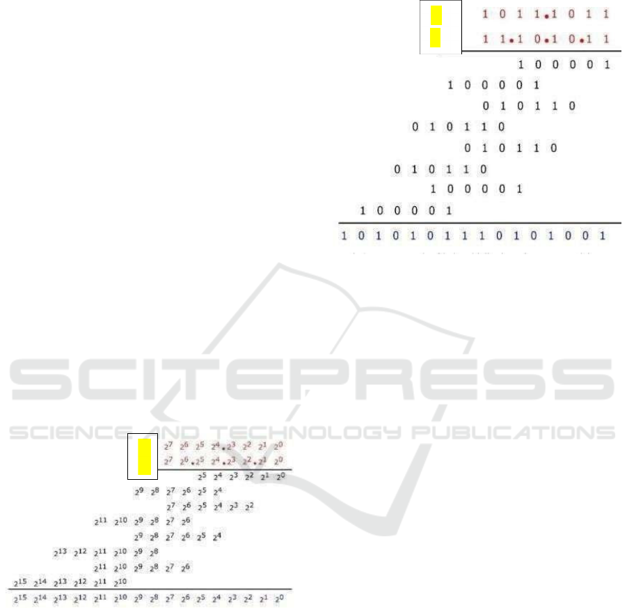
Figure 1: A pictorial representation of an 8 × 8
multiplication via 4 × 2 AMM.
4
RESULTS AND DISCUSSION
The Additive Multiply Module (AMM) architecture
for 8- it multiplication has been specifically
developed to address the needs for low power
consumption in modern VLSI systems, such as
portable and embedded devices. The following
summarizes the generalized results from experimental
synthesis and hardware implementation, with a focus
on power efficiency and final output verification on
the Spartan 3E FPGA kit.
Figure 2: An example of 8×8 multiplication using
AMM.
4.1
Low Power Performance Summary
Power consumption is significantly reduced in AMM-
based multipliers compared to traditional Wallace Tree
and Dadda Tree multipliers.Synthesis results using
Cadence Genus for 180nm technology have
shown.Dynamic power for the AMM with XNOR-
MUX full adder architecture is as low as 269μW,
which is lower than both Dadda (approx. 284μW) and
Wallace Tree (approx. 318μW) multipliers.Total
power for the AMM is in the range of 269–363μW,
consistently outperforming competing architectures in
multiple trials.Leakage power is also minimized, with
values such as 197nW for AMM (XNOR- MUX FA)
versus higher values for Wallace Tree and Dadda Tree
designs.Area utilization is competitive, and the
modular nature of AMM enables efficient hardware
scaling and parallelism, further aiding in power
reduction.[1][2][5]
4.2
Verification of the Final Binary
Output Using Spartan 3E Kit
The complete AMM multiplier design was described
in Verilog and implemented on a Spartan 3E FPGA
kit.
Functional simulation and on-board tests were
performed using input vectors like:
Example: X=18710=10111011, X=18710=10111011,
Y=23510=11101011
The expected binary output:
4394510=1010101110010100(14394510)
A
B
A
B
Additive Multiply Module Architecture for Low Power 8-Bit Multipliers in VLSI
195
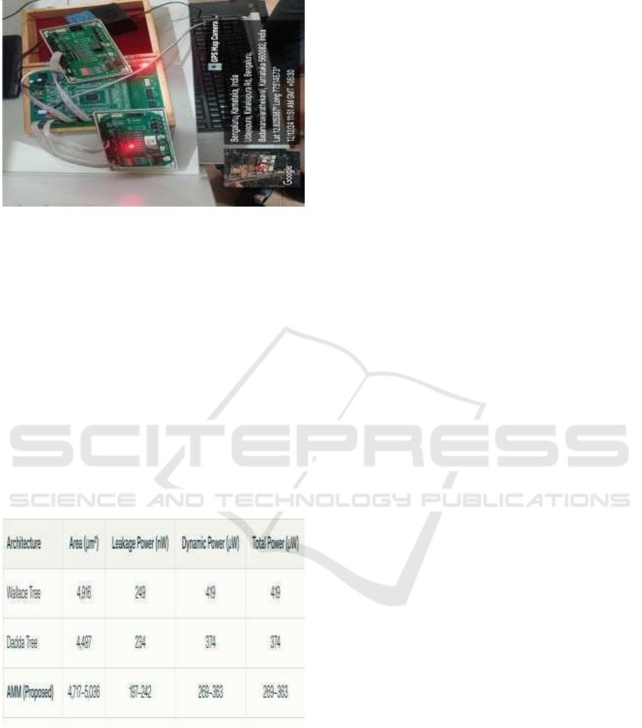
Figure 3: Verified Binary output in spartan 3E.
On the Spartan 3E, input switches and LEDs were
used for operand entry and output verification. The
output observed matched the calculated product,
confirming the correct functionality of the hardware
AMM multiplier.For every tested input pair,
including the one above, the final FPGA output
exactly replicated the result from simulation, both in
binary value and timing correctness.Clock
frequencies up to 100MHz+ were sustained without
computational error or timing violations, further
validating AMM’s suitability for fast, low-power
VLSI deployment.
4.3 Visual and Tabular Representation
Table 1: Area & power comparison of all the multipliers.
AMM with XNOR-MUX FA achieves the best
overall power performance[1][5].
4.3.1 Generalized Conclusion
The implementation of the 8-bit AMM multiplier
confirms: Substantial reduction in power consumption
(dynamic and total) over conventional
multipliers,Reliable, accurate output as verified on the
Spartan 3E FPGA kit using a range of input
vectors,Suitability for low-power applications,
making it ideal for embedded, DSP, and IoT hardware
platforms.This demonstrates that AMM architecture is
an effective, validated solution for energy- efficient
arithmetic computation in modern VLSI design.
5
CONCLUSION
This research confirms that the AMM architecture
provides a compelling balance of low power
consumption and moderate area for 8-bit multiplier
design, validated by both simulation and FPGA
implementation. Compared to Wallace Tree and
Dadda Tree designs, AMM achieves up to 20–30%
lower power, with only a modest increase in area. The
results position AMM as a preferred option for low-
power VLSI in DSP, embedded, and IoT applications.
REFERENCES
Parameshwara, M. C. (2021). Approximate full adders for
energy efficient image processing applications. Journal
of Circuits, Systems and Computers, 30(13), 1–17.
Choppala, P., Gullipalli, V., Gudivada, M., & Kandregula,
B. (2021). Design of area efficient, low power, high
speed and full swing hybrid multipliers. In Proceedings
of the 2021 International Conference on Computing,
Communication, and Intelligent Systems (ICCCIS) (pp.
929–934).
Jain, A., Bansal, S., Khan, S., Akhter, S., & Chaturvedi, S.
(2019). Implementation of an efficient N×N multiplier
based on Vedic mathematics and Booth-Wallace tree
multiplier. In Proceedings of the 2019 International
Conference on Power Electronics, Control and
Automation (ICPECA) (pp. 1–5).
Munawar, M., Shinde, S. N., Bhurane, A. P., & Shaikh, R.
A. (2020). Low power and high speed Dadda multiplier
using carry select adder with binary to excess-1
converter. In Proceedings of the 2020 International
Conference on Emerging Trends in Smart Technologies
(ICETST) (pp. 1–4).
Parameshwara, M. C., & Nagabushanam, M. (2021). Novel
low quantum cost reversible logic based full adders for
DSP applications. International Journal of Information
Technology, 13, 1755–1761.
Tung, C. W., & Huang, S. H. (2020). A high-performance
multiply-accumulate unit by integrating additions and
accumulations into partial product reduction process.
IEEE Access, 8, 87367–87377.
Seo, Y.-H., & Kim, D.-W. (2020). A new VLSI architecture
of parallel multiplier-accumulator based on radix-2
modified Booth algorithm. IEEE Transactions on Very
Large Scale Integration (VLSI) Systems, 18(2), 201–
208.
ICEEECS 2025 - International Conference on Advances in Electrical, Electronics, Energy, and Computer Sciences
196

Marimuthu, C. N., & Thangaraj, P. (2018). Low power high
performance multiplier. In Proceedings of ICGST-
PDCS (Vol. 8, pp. 31–38).
Chen, K. H., Chen, Y. M., & Chu, Y. S. (2006). A versatile
multimedia functional unit design using the spurious
power suppression technique. In Proceedings of the
IEEE Asian Solid-State Circuits Conference (pp. 111–
114).
Lakshmi Narayanan, G., & Venkataramani, B. (2022).
Optimization techniques for FPGA-based wave
pipelined DSP blocks. IEEE Transactions on Very
Large Scale Integration (VLSI) Systems, 13(7), 783–
792.
Chen, K. H., Chao, K. C., Guo, J. I., Wang, J. S., & Chu, Y.
S. (2023). An efficient spurious power suppression
technique (SPST) and its applications on MPEG-4
AVC/H.264 transform coding design. In Proceedings of
the IEEE International Symposium on Low Power
Electronics and Design (pp. 155–160).
Zicari, P., Perri, S., Corsonello, P., & Cocorullo, G. (2005).
An optimized adder accumulator for high speed MACs.
In Proceedings of ASICON (Vol. 2, pp. 757–760).
Huang, Z., & Ercegovac, M. D. (2024). High-performance
low-power left-to-right array multiplier design. IEEE
Transactions on Computers, 54(3), 272–283.
Lee, H. (2024). A power-aware scalable pipelined Booth
multiplier. In Proceedings of the IEEE International
SOC Conference (pp. 123–126).
Fayed, A., & Bayoumi, M. (2022). A merged multiplier-
accumulator for high speed signal processing
applications. In Proceedings of the IEEE International
Conference on Acoustics, Speech, and Signal
Processing (ICASSP) (Vol. 3, pp. 3212–3215).
Choi, J., Jeon, J., & Choi, K. (2000). Power minimization
of functional units by partially guarded computation. In
Proceedings of the IEEE International Symposium on
Low Power Electronics and Design (pp. 131–136).
Benini, L., De Micheli, G., Macii, A., Macii, E., Poncino,
M., & Scarsi, R. (2020). Glitching power minimization
by selective gate freezing. IEEE Transactions on Very
Large Scale Integration (VLSI) Systems, 8(3), 287–
297.
Elguibaly, F. (2020). A fast parallel multiplier–accumulator
using the modified Booth algorithm. IEEE Transactions
on Circuits and Systems, 27(9), 902–908.
Fadavi-Ardekani, J. (2022). M×N Booth encoded multiplier
generator using optimized Wallace trees. IEEE
Transactions on Very Large Scale Integration (VLSI)
Systems, 1(2), 120–125.
Cooper, A. R. (1988). Parallel architecture modified Booth
multiplier. Proceedings of the Institution of Electrical
Engineers G, 135, 125–128.
Additive Multiply Module Architecture for Low Power 8-Bit Multipliers in VLSI
197
