
An Asymmetric Minimal Component Count Three-Phase Multilevel
Converter Suitable for PV Applications
Samuel Nii Tackie
1
, Zubeir Mohamed Nur
1
, Ozgur Cemal Ozerdem
1
and William Olurotimi Falana
2
1
Department of Electrical and Electronic Engineering, Near East University, Nicosia, Northern Cyprus, Cyprus
2
Centre for Science, Technology and Engineering (BILTEM) Researchers, Near East University,
Nicosia, Northern Cyprus, Cyprus
Keywords: Asymmetric Multilevel Inverter, Three-Phase Multilevel Inverter, Minimal Component Count, Total Standing
Voltage.
Abstract: Multilevel inverters' well-enhanced DC-AC power conditioning feature makes them suitable for medium and
high-power applications such as grid-tied PV systems. This paper proposes an asymmetrical three-phase
multilevel inverter with minimal component count. The proposed three-phase topology is an improved
architecture derived from the conventional H-bridge by incorporating extra switches and a DC source, thus
resulting in a minimal component count structure. The system achieves 31-levels of load voltage, and the
components employed per phase are 12 switches, 12 driver circuits, and 6 DC input sources. The proffered
three-phase topology employs an extension technique in its connection to minimize the DC source
components by a factor of 2. Increasing the phase count minimizes the voltage count significantly. The
remarkable benefits of the presented inverter are higher voltage levels, high-quality output waveforms,
reduced total standing voltage (TSV), minimized switching losses, less installation space, and reduced cost.
The inverter’s control technique is based on the fundamental frequency control method. Analysis of the
topology’s components usage was conducted and compared to existing recent topologies. PSCAD/EMTDC
software is used for the simulation, and the results validate the TSV and the performance of the inverter.
1 INTRODUCTION
The surge in demand for electrical power and the
integration of distributed generation systems into
today’s power grid have increased the demand for
power conditioning devices such as power electronic
converters, which are adaptable and efficient. One
such converter is the inverter, which transforms DC
power into AC power from sources like solar cells
and batteries.
Multilevel inverters are of great importance in the
power conditioning industry, meeting a lot of
demands in contrast to the traditional two-level
inverter that has the limitations of the inability to
operate at higher voltage levels and substantial
switching voltage stress (Islam et al, 2019. The
benefits of MLI include minimized harmonic
distortions, reduced switching losses, decreased
electromagnetic interferences, higher output voltage
levels, and high-quality waveforms (Tackie and
Babaei, 2019), (Krishnan et al, 2018). MLI strives to
generate a load voltage waveform that closely mimics
the sinusoidal waveform, which increases power
quality and reduces the stress placed on
semiconductor switches. MLI is used in highly
efficient renewable energy systems, electric vehicles,
HVDC, power transmission systems, and dynamic
voltage restorers (Uthirasamy et al, 2018), (Sekar et
al, 2017), (Hammami et al, 2018), (Seth et al, 2017).
The conventional classification of multilevel inverter
topologies is grouped into three types defined as
Cascaded H-Bridge (CHB), Neutral-point Clamped
(NPC), and Flying Capacitor (FC) multilevel
inverters (Ye et al, 2014), (Li et al, 2011), (Schettino
et al, 2019). However, these topologies still have
limitations, considering that the components used can
be quite high. For example, the DC sources used in
cascaded H-bridge MLI are higher, while NPC MLI
requires lots of clamping diodes, FC MLI uses many
clamping capacitors. Adding more components
makes the system bulkier, more complex, and less
reliable, and increases the cost. Studies show that
researchers are working to improve these topologies
to mitigate these disadvantages and ultimately
Tackie, S. N., Nur, Z. M., Ozerdem, O. C. and Falana, W. O.
An Asymmetric Minimal Component Count Three-Phase Multilevel Converter Suitable for PV Applications.
DOI: 10.5220/0014288800004848
Paper published under CC license (CC BY-NC-ND 4.0)
In Proceedings of the 2nd International Conference on Advances in Electrical, Electronics, Energy, and Computer Sciences (ICEEECS 2025), pages 153-163
ISBN: 978-989-758-783-2
Proceedings Copyright © 2026 by SCITEPRESS – Science and Technology Publications, Lda.
153

enhance the performance of the system (Aalami et al,
2018), (Ali et al, 2024). The cascaded H-bridge MLI
is preferred amongst the three classical topologies
because they don’t require clamping capacitors or
diodes to regulate the voltage output, and it does not
require complex control.
The input voltage sources can vary depending on
the scope of the inverter design and its purpose. There
are two categories of CHB MLIs: symmetric and
asymmetric. Considering the voltage input sources, if
they are all equal in magnitude, it is called a
symmetric topology. Topologies with different input
sources are called asymmetric. The differences in
magnitudes give the asymmetrical topology an
advantage in achieving the desired high output
voltage level without adding more structural units and
voltage sources, as compared to the symmetric
configuration. Furthermore, the space required for
installing the asymmetric topology is less, and it costs
less than the symmetric cascaded topology (Dixon et
al, 2010).
Reviewing recent trends in the literature,
researchers are focused on advancing the structure of
MLI topologies by reducing component count as well
as providing simpler control techniques. The authors
in (Babaei et al, 2014) presented a cascaded
multilevel inverter topology with reduced switches,
using 6 unidirectional power switches and 2 input
voltage sources to generate 7-level output. The study
presented in (Dhanamjayulu et al, 2020) describes a
three-phase MLI with asymmetric magnitudes, which
generates a 19-levels output voltage. It features 13
switches and 3 DC input sources per phase, resulting
in a reduction in components and lowering the total
harmonic distortions. Another topology that employs
bidirectional switches, leads to an increase in IGBTs,
and a rise in cost is presented by (Mekhilef and Kadir,
2010). A conventional NPC MLI is presented in
(Panda et al, 2018) that is connected to the PV system;
however, it requires an additional regulator to ensure
the potential difference is preserved along the
capacitors. The paper (Phanikumar and Agarwal,
2018) gives a single-phase asymmetric topology,
which generates 17-levels. The components
employed are 11 switches and 2 sources; the topology
has lower conduction losses by utilizing just four
switches that conduct in each state. Reference
(Memon et al, 2024) details a 17-level asymmetric
topology for PV systems that has reduced
components and less voltage stress on the system. It
has distributed the stress across the switches, and the
inverter works with different loads. A switched
diode-based multilevel inverter topology with fewer
components was developed in (Sathik et al, 2020);
however, the switches experienced high-standing
voltages. A crucial part of the system is selecting a
control method, as it strongly affects the inverter’s
performance. The control technique determines the
switching strategy, which, depending on the design
objectives, can minimize the losses and total
harmonics distortions (Hasan et al, 2017).
This paper proffers a new asymmetrical three-
phase multilevel inverter topology that minimizes
component count while achieving higher output
levels. The topology is suitable for medium- and
high-power applications, such as photovoltaic
applications. The proposed topology generates 31-
levels of voltage steps employing 12 switches and 6
DC sources per phase. An extension technique is used
for the three-phase topology connection to reduce the
DC sources in total, thereby reducing the total
component count. The topology generates a line-to-
line voltage of 61-levels for the three phases. The FF
control method is used, and the simulation is carried
out in PSCAD/EMTDC. An analysis of the
component count of the proposed topology
juxtaposed to existing recent topologies is conducted,
highlighting the merits of the inverter. The simulation
results for the load output and the total standing
voltages of the switches are illustrated. The structure
of the paper is outlined as follows: Section 2 features
the proposed three-phase asymmetrical multilevel
inverter, inverter losses, the total standing voltage,
and comparative analysis. In Section 3, the simulation
parameters and results are provided. Section 4 is the
discussion, and Section 5 is the conclusion.
2 PROPOSED METHOD
2.1 Proposed Setup
The proposed topology is an improved version of the
conventional three-phase H-bridge multilevel
inverter. The H-bridge structure allows for the
generation of both positive and negative voltage
levels. Additional H-bridge units, switches, and DC
sources are incorporated into the conventional H-
bridge structure to derive the presented topology. The
proposed asymmetric minimal component count
three-phase H-bridge multilevel inverter entails a per-
phase component of 12 power switches, four of which
are bidirectional, and 6 input voltage sources. The
proposed three-phase MLI consists of 36 power
switches, twelve of which are bidirectional, and 18 DC
sources. Bidirectional switches can block voltage in
both polarities and are constructed using two IGBTs
and two antiparallel diodes, while unidirectional
ICEEECS 2025 - International Conference on Advances in Electrical, Electronics, Energy, and Computer Sciences
154
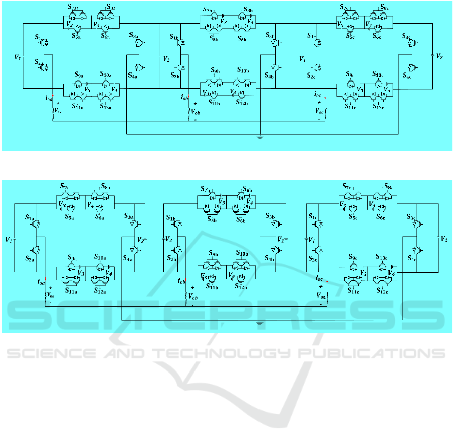
Figure 1. The proposed three-phase multilevel inverter.
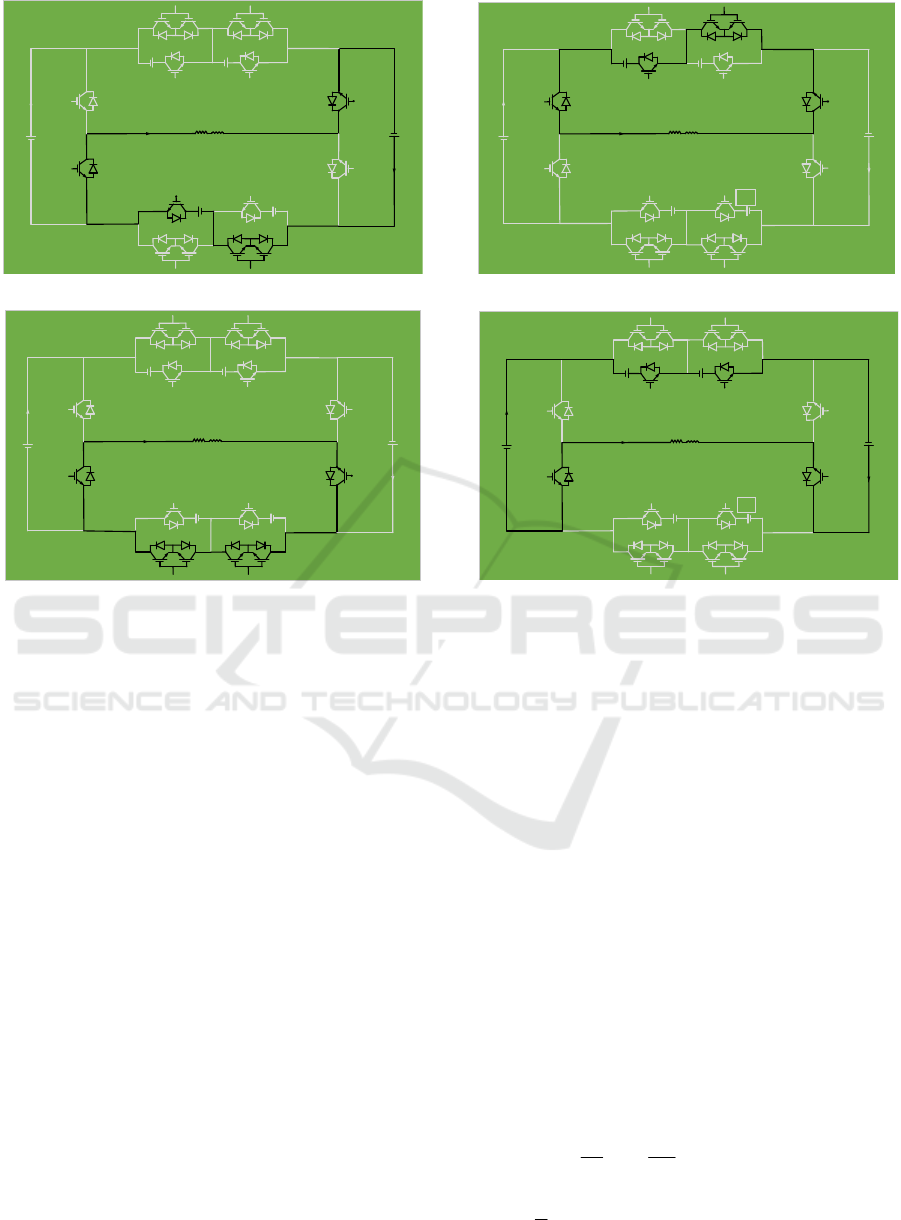
Figure 2. The proposed three-phase mli without extension technique.
switch blocks the voltage in one direction and are
simply constructed with one IGBT and diode
connected in parallel. The load of the system is the
resistance-inductance (RL) load. Figure 1 illustrates
the proposed three-phase multilevel inverter.
The structure of the proposed topology per phase,
compared to the conventional H-bridge inverter,
includes several additions. Two structural units are
added to the upper and bottom sections of the
inverter, with two sources in each unit. The top unit
has two bidirectional switches, S
7a
and S
8a
, and the
two DC sources are V
3
and V
4
. In the bottom unit, the
bidirectional switches are S11a and S
12a
. The two
structural units allow for the generation of positive
and negative levels; the bottom structural unit
generates positive levels, and the top structural unit
produces negative levels for phase A. The same is
replicated for the remaining phases, i.e., phase B and
phase C, accordingly. The switch labeling changes to
S
7b
, S
8b
, S
11b
, and S
12b
for phase B, while S
7c
, S
8c
, S
11c
,
and S
12c
relate to phase C. However, the DC voltage
sources V
3
and V
4
remain the same for all phases,
with identical magnitudes.
In addition to the two structural units, there is an
extra voltage source on the right side of each phase.
The extension technique of the configuration reduces
the DC source for each phase; instead of separate DC
sources, each phase shares a common DC source with
the adjacent phase. Phase B shares the DC source V
2
with phase A on its left side and the V
1
source with
phase C on its right side. An extension technique is
used in the configuration of the proposed three-phase
multilevel inverter, which minimizes the component
count of the DC sources; it reduces the total DC
sources by a factor of 2.
The levels and component count of the three-
phase proposed topology are expressed in equation
(1), and Figure 2 shows the same proposed topology
without the extension technique, i.e., individual phase
configuration. An asymmetric configuration is
utilized to achieve higher output voltage levels. This
characteristic makes the inverter suitable for PV
applications because of the varying magnitudes of DC
sources generated by PV systems. If symmetric
topology were used, only nine voltage levels would
be generated. The proposed topology employs DC
An Asymmetric Minimal Component Count Three-Phase Multilevel Converter Suitable for PV Applications
155
sources of different magnitudes, arranged in series to
raise the levels and generate a high-quality output
waveform that closely mimics a sinusoidal waveform.
The magnitudes of the DC sources and the maximum
output voltage of the topology are given in equation
(2). The proposed topology generates a maximum of
31-levels of output voltage when using asymmetric
DC sources.
31
16
36
36
48
Level
Sources
Switches
Driver
IGBT
N
N
N
N
N
=
=
=
=
=
(1)
1,
2,
35 ,
46 ,
,max ,
1
2
4
8
15
dc in
dc in
dc in
dc in
odcin
VV
VV
VV V
VV V
VV
=
=
==
==
=
(2)
Table 1 details the switching states for the 31-levels
of phase A of the topology. The switches that are
switched on depend on which voltage sources are
activated to generate a specific voltage level. As
shown in Table 1, to generate a positive 15V
dc
, the
voltage sources
V
1
, V
2
, V
3,
and V
4
are activated,
and the switches turned on are S
1a
, S
3a
, S
9a
, and S
10a
.
For 14 positive level sources,
V
2
, V
3,
and V
4
are
activated, and the switch path to follow is S
2a
, S
3a
, S
9a
,
and S
10a
. Negative 5 voltage level -5V
dc
, the switches
S
2a
, S
3a
, S
5a
, S
8a
. Figure 3 shows selected active
switches and current paths considering the switching
states of phase A. For example, in Figure 3a, to
generate 6V
dc,
the closed loop of the load follows a
path that takes the switch pattern passing switches S
2a
,
S
3a
, S
9a,
and S
12a
. Each conducting switch displays a
certain voltage level, and when one state is
conducting, the other states are off. However, there’s
a situation to be avoided; some switches cannot be
turned on simultaneously, as they will cause a short
circuit of the voltage sources.
For example, switches (S
1a
, S
2a
), (S
3a
, S
4a
), (S
5a
,
S
7a
), (S
6a
, S
8a
), (S
9a
, S
11a
), and (S
10a
, S
12a
) for phase A
are also similar for phase B and phase C switches. For
a 0V output in phase A, there are two states: switches
S
2a
, S
4a
, S
11a
, S
12a
, or S
1a
, S
3a
, S
5a
, and S
6a
are switched
on. The switching states for phase A and phase C are
similar. In phase C, to generate 15V
dc
, switches S
1c
,
S
3c
, S
9c
, and S
10c
are gated on, just like in phase A.
However, in Phase B, switches S
2b
, S
4b
, S
5b,
and S
6b
Table 1. Switching pattern for phase A.
Level Switches ON Input Sources V
Output
1 S
1a
, S
3a
, S
9a
, S
10a
V
1
+V
2
+V
5
+V
6
15V
dc,in
2 S
2a
, S
3a
, S
9a
, S
10a
V
2
+V
5
+V
6
14V
dc,in
3 S
1a
, S
4a
, S
9a
, S
10a
V
1
+V
5
+V
6
13V
dc,in
4 S
2a
, S
4a
, S
9a
, S
10a
V
5
+V
6
12V
dc,in
5 S
1a
, S
3a
, S
10a
, S
11a
V
1
+V
2
+V
6
11V
dc,in
6 S
2a
, S
3a
, S
10a
, S
11a
V
2
+V
6
10V
dc,in
7 S
1a
, S
4a
, S
10a
, S
11a
V
1
+V
6
9V
dc,in
8 S
2a
, S
4a
, S
10a
, S
11a
V
6
8V
dc,in
9 S
1a
, S
3a
, S
9a
, S
12a
V
1
+V
2
+V
5
7V
dc,in
10 S
2a
, S
3a
, S
9a
, S
12a
V
2
+V
5
6V
dc,in
11 S
1a
, S
4a
, S
9a
, S
12a
V
1
+V
5
5V
dc,in
12 S
2a
, S
4a
, S
9a
, S
12a
V
5
4V
dc,in
13 S
1a
, S
3a
, S
11a
, S
12a
V
1
+V
2
3V
dc,in
14 S
2a
, S
3a
, S
11a
, S
12a
V
2
2V
dc,in
15 S
1a
, S
4a
, S
11a
, S
12a
V
1
1V
dc,in
16 S
2a
, S
4a
, S
11a
, S
12a
- 0
16 S
1a
, S
3a
, S
7a
, S
8a
- 0
17 S
2a
, S
3a
, S
7a
, S
8a
-V
1
-1V
dc,in
18 S
1a
, S
4a
, S
7a
, S
8a
-V
2
-2V
dc,in
19 S
2a
, S
4a
, S
7a
, S
8a
-(V
1
+V
2
) -3V
dc,in
20 S
1a
, S
3a
, S
5a
, S
8a
-V
3
-4V
dc,in
21 S
2a
, S
3a
, S
5a
, S
8a
-(V
1
+V
3
) -5V
dc,in
22 S
1a
, S
4a
, S
5a
, S
8a
-(V
2
+V
3
) -6V
dc,in
23 S
2a
, S
4a
, S
5a
, S
8a
-(V
1
+V
2
+V
3
) -7V
dc,in
24 S
1a
, S
3a
, S
6a
, S
7a
-V
4
-8V
dc,in
25 S
2a
, S
3a
, S
6a
, S
7a
-(V
1
+V
4
) -9V
dc,in
26 S
1a
, S
4a
, S
6a
, S
7a
-(V
2
+V
4
) -10V
dc,in
27 S
2a
, S
4a
, S
6a
, S
5a
-(V
1
+V
2
+V
4
) -11V
dc,in
28 S
1a
, S
3a
, S
5a
, S
6a
-(V
3
+V
4
) -12V
dc,in
29 S
2a
, S
3a
, S
5a
, S
6a
-(V
1
+V
3
+V
4
) -13V
dc,in
30 S
1a
, S
4a
, S
5a
, S
6a
-(V
2
+V
3
+V
4
) -14V
dc,in
31 S
2a
, S
4a
, S
5a
, S
6a
-(V
1
+V
2
+V
3
+V
4
) -15V
dc,in
are gated on. To generate a negative 5 level (-5V
dc
) in
phase B, the switches S
2b
, S
3b
, S
9b
, and S
12b
are turned
on.
The load voltage for phase A is denoted as
V
a
, for
phase B as
V
b,
and for phase C as V
c
. The line-to-line
voltages of the three-phase system are denoted by
V
ab
,
V
bc
, and V
ca
. The line-to-line voltage generates a
maximum of 61-level of output voltage. The equation
(3) expresses the line voltages as follows:
–
–
–
ab an bn
bc bn cn
ca cn an
VVV
VVV
VVV
=
=
=
(3)
ICEEECS 2025 - International Conference on Advances in Electrical, Electronics, Energy, and Computer Sciences
156
V
1
i
i
V
2
i
i
I
o
+ V
o
-
S
w1
S
w2
S
w3
S
w4
S
w9
S
w11
S
w12
S
w10
S
w7
S
w8
S
w6
S
w5
V
3
V
4
V
5
V
6
V
1
i
i
V
2
i
i
I
o
+ V
o
-
S
w1
S
w2
S
w3
S
w4
S
w9
S
w11
S
w12
S
w10
S
w7
S
w8
S
w6
S
w5
V
3
V
4
V
5
V
6
(a) 6V
dc
(b) -4V
dc
V
1
i
i
V
2
i
i
I
o
+ V
o
-
S
w1
S
w2
S
w3
S
w4
S
w9
S
w11
S
w12
S
w10
S
w7
S
w8
S
w6
S
w5
V
3
V
4
V
5
V
6
V
1
i
i
V
2
i
i
I
o
+ V
o
-
S
w1
S
w2
S
w3
S
w4
S
w9
S
w11
S
w12
S
w10
S
w7
S
w8
S
w6
S
w5
V
3
V
4
V
5
V
6
(c) 0V (d)-15V
dc
Figure 3. Switching states for the proposed topology phase A.
2.2 Standing Voltage
A key factor in determining the overall cost of an
inverter is the blocking voltage of the switches and the
diversity of the DC sources. A switch with low power
ratings is preferred because it reduces the voltage
stress on the switches and minimizes power losses.
The peak voltage that a semiconductor switch can
block in its off state is referred to as the blocking
voltage. The sum of all the individual blocking
voltages of the switches is the blocking voltage of the
inverter system. The proposed asymmetric three-
phase multilevel inverter uses 12 power switches per
phase: 8 unidirectional switches and 4 bidirectional
switches, which are expressed in equation (4). The
blocking voltage of the total switches in the three-
phase inverter is three times the sum of the blocking
voltage for one phase, and it is expressed in equation
(6).
12 ,
34 ,
57911 ,
6 8 10 12 ,
2
4
8
Sa S a dcin
Sa Sa dcin
Sa Sa Sa S a dcin
Sa Sa Sa Sa dcin
VV V
VV V
VVVV V
VVV V V
==
==
=== =
== = =
(4)
()( )
1, ,,
23 412 54
dc in dc in dc in
VV V V
φ
=+ =
(5)
()
3,,
3 54 162
dc in dc in
VV V
φ
==
(6)
2.3 Power Losses
Inverter power losses are largely attributable to two
losses in the switches: switching losses and
conduction losses. Blocking voltage losses also
occur, but they are negligible and are not considered.
Switching losses occur in both states, and the
summation of the losses during the on-state and the
losses during the off-state gives the total switching
losses. The total switching loss P
SW
is given in
equation (7). E
on
is the turn-on losses, E
off
is the turn-
off losses, V
SW
is the off-state voltage, I is the current
prior to turning on, and I' is after it is on.
()
0
'
0
'
()()
1
6
on
on
t
on
t
sw
on on
on on
on sw on
Evtitdt
V
I
Etttdt
tt
EVIt
=
=−−
=
(7)
An Asymmetric Minimal Component Count Three-Phase Multilevel Converter Suitable for PV Applications
157

()
0
0
1
()()
6
1
6
off
off
t
off sw on
t
sw
off off
off off
on sw off
EvtitdtVIt
V
I
Etttdt
tt
EVIt
==
=−−
=
(8)
1
11
off
on
switch
N
N
N
SW s on off
k
ii
Pf E E
=
−−
=+
(9)
Conduction losses occur during the on-state. The
losses of the IGBT and the diode of the switch give
the conduction losses, and their sum is the total
conduction losses. The proposed topology consists of
bidirectional switches, which equate to more IGBTs
and diodes. P
C,T
is the losses for the transistor IGBT,
and P
C,D
is the diode losses. R
T
, V
T
denotes the
resistance and the forward voltage drop for the
transistor, while R
D,
V
T
is for the diode resistance and
voltage drop. The total conduction loss is noted as P
C
.
The total power losses of the inverter, denoted by P
C,
and the efficiency
η
are given in the equations
below:
,
2
,
0
()
1
() (
(
2
)()
()() )
TT
TTTT
CT
C
Pit
Pd
VR tit
VRi itttnt
β
β
π
ω
π
+
+
=
=
(10)
[
]
[]
,
2
,
0
(
1
)
)
()
() (
()
()()
2
CD D D
CD D DD
P
t
t
Pn
VRitit
VR diittt
π
ω
π
+
+
=
=
(11)
,,CCTCD
PP P=+
(12)
The total loss of the inverter is given by equation (13),
which sums up the switching losses and conduction
losses. The Inverter’s efficiency is calculated as the
ratio of power output to power input, as expressed in
equation (14).
L
osses SW C
P
PP=+
(13)
out
input
P
P
η
=
(14)
2.4 Comparison Study
A comparative analysis of the presented topology
with other topologies is detailed in this section. The
analysis focuses on the component count of the
proposed three-phase circuit topology. The
topologies all have 31-step voltage levels. The focus
is mainly on the IGBTs, diodes, DC sources, and
driver circuits. Topologies with more components
tend to have higher costs, require more space, and
have less efficiency. The proposed topology has both
unidirectional and bidirectional switches; it has 12
power switches. The presented topology uses 4
bidirectional switches, which means it has more
IGBTs and diodes than the drivers, as a common
emitter driver is used. A total of 12 drivers are
utilized, 16 IGBTs, and 16 diodes. Table 2 has
a component comparison of the proposed topology
per phase to other existing topologies. The proposed
inverter has 6 DC sources, the second highest among
all topologies, only topology (Kubendran et al, 2024)
and CHB conventional topologies having more.
However, the proposed topology has the second-
fewest total components behind only topology
(Tackie et al, 2023). A bar chart comparing the
topologies in Table 2 is illustrated in Figure 4. The
proposed inverter is among the topologies with
minimal component counts.
Table 2: Comparative topologies analysis of single-phase.
Topology [P] [22] [23] [24] [25] [26]
Voltage
Level
31 31 31 31 31 31
DC
Source
6 15 2 2 4 4
Switches
IGBT
16 18 16 18 16 12
No.
Drive
r
12 18 16 18 16 12
Diode 16 32 18 20 16 12
Clamped
Diode
0 0 0 0 0 0
Capacitor 0 0 4 4 0 0
Clamped
Capacito
r
0 0 0 0 0 0
Total
Componen
t
50 83 56 62 52 40
Note: [22]- (Kubendran et al, 2024), [23] -(Roy et al, 2019), [24]-
(Ahmad et al, 2020), [25] -(Chinthamalla, 2017), [26] -(Tackie et
al, 2023)
ICEEECS 2025 - International Conference on Advances in Electrical, Electronics, Energy, and Computer Sciences
158
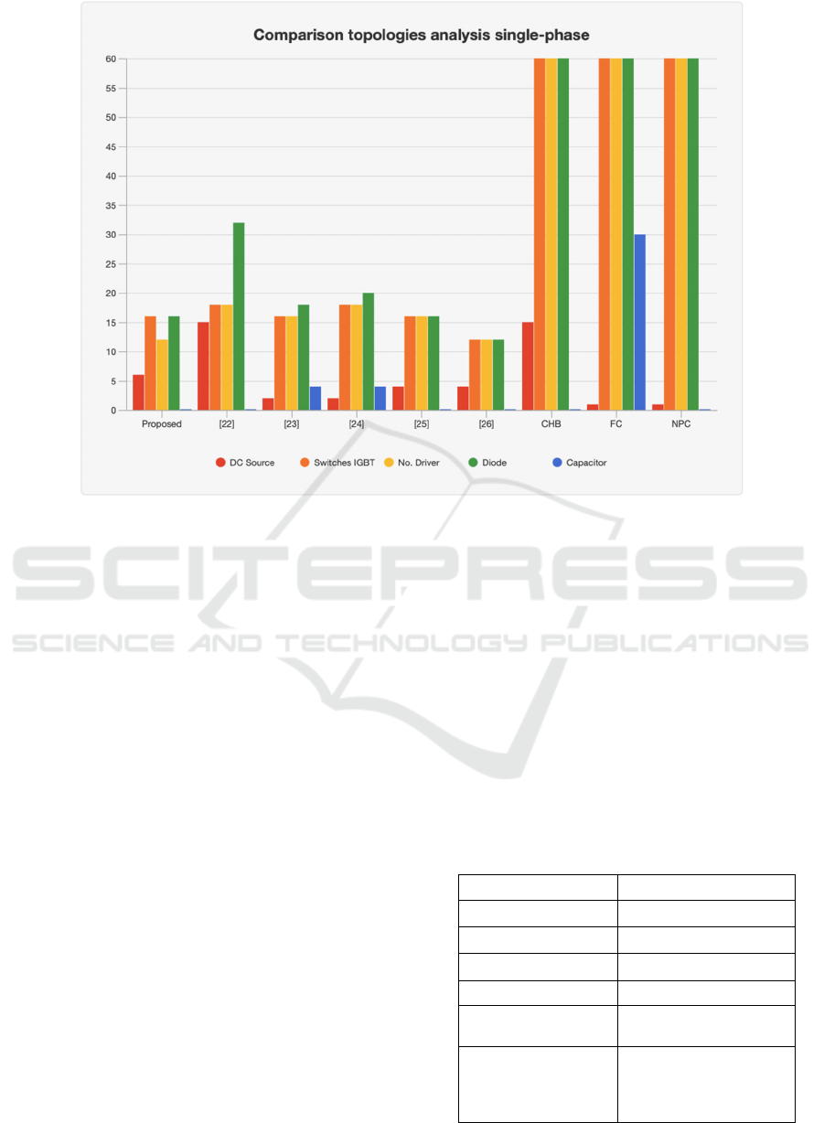
Figure 4. Comparative analysis per-phase
It’s apparent that the proposed topology achieves an
optimal cost-benefit when the component count is
compared to the output voltage level generated. It
utilizes low-power-rated switches, contributing to a
more efficient system. The bar chart also includes the
conventional multilevel inverters, which have the
highest component counts. The proposed topology
has 16 diodes per phase, the same as the topology
(Chinthamalla, 2017), which is lower than the
topologies (Kubendran et al, 2024), (Roy et al, 2019),
(Ahmad et al, 2020). The number of driver circuits in
the proposed topology is the lowest, along with
the topology (Tackie et al, 2023).
3 RESULTS
The simulation is conducted using PSCAD. The
presented asymmetrical three-phase multilevel
inverter has a resistance inductance (RL) load. The
components include 12 switches, of which 4 are
bidirectional switches and 6 input sources per phase.
Simulation is provided to validate the effectiveness of
the inverter. The fundamental frequency control
method is used for the switching control technique,
offering some benefits such as lower switching
losses, simpler phase control, and phase shifts of 120
degrees, in contrast to other control techniques. Phase
B is shifted by 120 degrees, and phase C is 240
degrees phase shifted. Table 3 outlines the parameters
that are used for the simulation, including the
asymmetric DC sources. The resistive-inductive load
parameters are 50Ω for resistance and 0.055H for
inductance.
A modulation index of 1 is selected, and the
modulation index has effects on the results, as it
determines the peak of the voltage in comparison with
the reference signal, and affects the harmonic
distortion. Higher modulation means higher output
voltage. It is selected as ‘1’; more than that will cause
overmodulation and distortions in output waveforms.
Table 3. Simulation configurations.
Variables Magnitude
Output Frequency 50Hz
Output Resistance 50Ω
Modulation Index 1
Output Inductance 0.055H
Switching
Frequency
5kHz
Input DC Sources
V
1
= 16V, V
2
= 32V,
V
3
= 64V, V
4
= 128V,
V
5
= 64V, V
6
= 128V
An Asymmetric Minimal Component Count Three-Phase Multilevel Converter Suitable for PV Applications
159
A switching frequency of 5kHz is selected; while
a higher frequency equates to good output
waveforms, it also leads to more losses; the aim is to
balance it, as our objective is better power quality. For
the asymmetric voltage sources, the initial source is
chosen as
V
1
= 16V. The incremented voltage step is
16V, so
V
2
is 32V, which is double V
1
. V
3
and are
64V; they have the same magnitudes to generate
the same steps of positive and negative levels, similar
to
V
4
and V
6,
which have 128V. The peak output phase
voltage consists of 15 distinct levels of 16V, resulting
in a peak output phase voltage of 240V. The phase
voltages
V
a
, V
b,
and V
c
feature 31-stepped voltage
levels with a peak value of 240V.
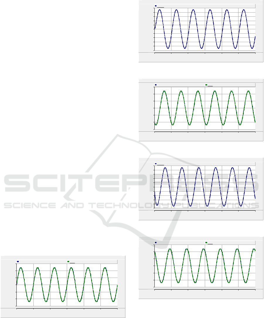
Figure 5 illustrates the stepped load output
voltage waveform, along with the reference signal for
phase A, ‘Refa’. The output voltage aligns with the
reference signal and generates a high-quality
waveform. Figure 6 is the phase A output current,
with a peak of 4.4A. Figure 7 presents the voltage
waveform result and the reference signal for phase B,
V
b,
and Refb, while Figure 8 displays the phase
current
I
b
for phase B. The results show a 120-degree
phase shift compared to the phase A load outputs.
Phase B output voltage also reaches a peak value of
240V. Phase C results waveforms are shifted by 240
degrees and are illustrated in Figures 9 and 10. The
line-to-line output voltage generated 61-levels, the
results for the line voltages; the line voltage between
phase A and phase B is
V
ab
. V
bc
is the line voltage
between phase B and phase C, and
V
ca
is the line
voltage from phase C to phase A. The result is
illustrated in Figure 11. The waveforms have phase
differences.
V
ab
is represented by the blue waveform,
V
bc
by the green waveform, and V
ca
by the red
waveform. The peak value of the line-to-line voltage
waveforms is 415V.
Figure 5. Phase A load voltage waveform.
Figure 6. Phase A current waveform.
Figure 7. Phase B load voltage waveform.
Figure 8. Phase B current waveform.
Figure 9. Phase C load voltage waveform.
0.000 0.020 0.040 0.060 0.080 0.100 0.120
-300
-200
-100
0
100
200
300
V_a [ V ] Re f a
Ma i n : G r a
p
hs
0.000 0.020 0.040 0.060 0.080 0.100 0.120
-5.0
-4.0
-3.0
-2.0
-1.0
0.0
1.0
2.0
3.0
4.0
5.0
y
I_a [A]
Ma i n : G r a
p
hs
0.000 0.020 0.040 0.060 0.080 0.100 0.120
-300
-200
-100
0
100
200
300
y
V_b [ V ] Re f b
Ma i n : G r a
p
hs
0.000 0.020 0.040 0.060 0.080 0.100 0.120
-5.0
-4.0
-3.0
-2.0
-1.0
0.0
1.0
2.0
3.0
4.0
5.0
y
I_b [A]
0.000 0.020 0.040 0.060 0.080 0.100 0.120
-300
-200
-100
0
100
200
300
V_c [ V ] Re f c
ICEEECS 2025 - International Conference on Advances in Electrical, Electronics, Energy, and Computer Sciences
160
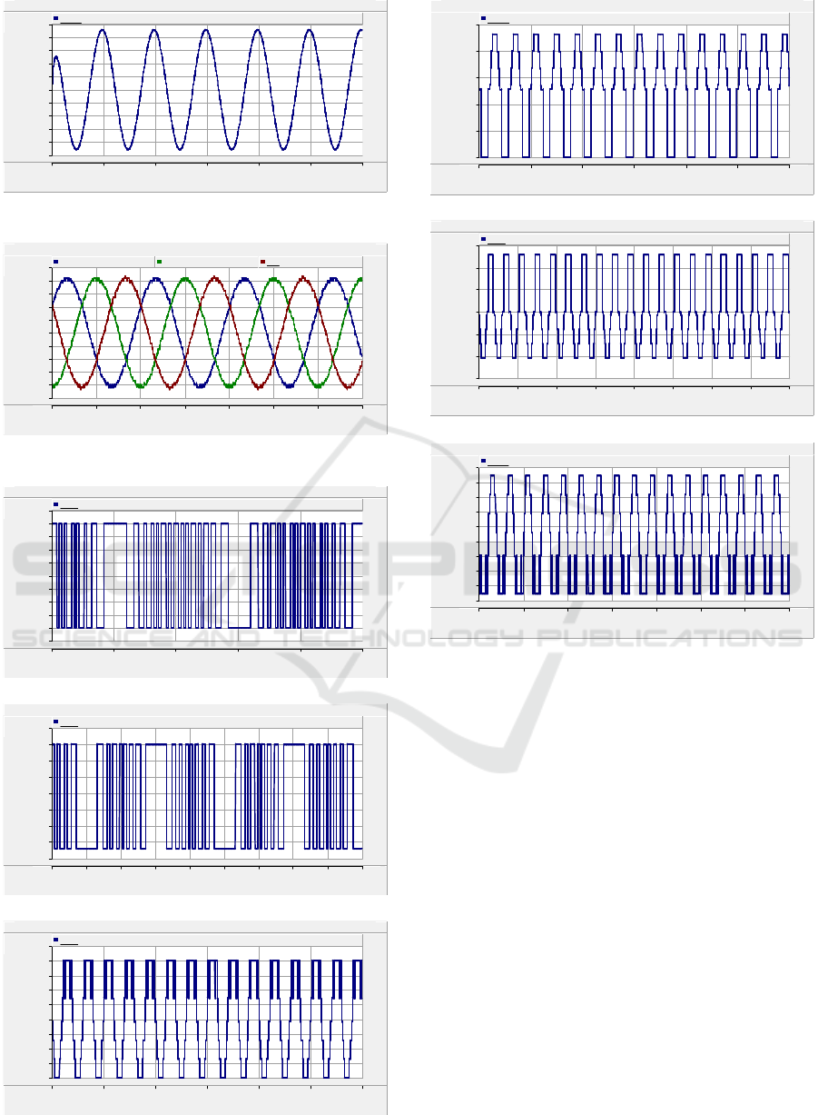
Figure 10. Phase C current waveform.
Figure 11. Line-to-line voltage waveforms.
(a)
(b)
(c)
(d)
(e)
(f)
Figure 12. Standing Voltages of switches in phase A; (a)
standing voltage of switch S
1a
; (b) TSV of switch S
4a
; (c)
TSV of switch S
5a
; (d) TSV of switch S
8a
; (e) TSV of switch
S
10a
; (f) TSV of switch S
11a
.
The results of the standing voltage of phase A are
depicted in Figure 12. Switches S
1a
and S
2a
have
similar blocking voltage, and they are dependent on
the V
1
voltage source. The waveform results of S
1a
are illustrated as having a blocking voltage of 16V.
Switches S
3a
and S
4a
have the same blocking voltage
of 32V. The bidirectional switches S
7a
, S
8a
, S
11a,
and
S
12a
can block voltage in both polarities, which is
confirmed by the waveform results, i.e., the switches
blocking voltages having positive and negative
magnitudes. Switches S
5a
, S
7a
, S
9a
and S
11a
have
standing voltage of 62V. Switches S
6a
, S
8a
, S
10a
, and
S
12a
have standing voltage of 128V. The TSV for
phase A is 864V. The three-phase topology total
standing voltage, TSV, will be 2592V.
0.000 0.020 0.040 0.060 0.080 0.100 0.120
-5.0
-4.0
-3.0
-2.0
-1.0
0.0
1.0
2.0
3.0
4.0
5.0
I_c [A]
0.000 0.010 0.020 0.030 0.040 0.050 0.060 0.070
-500
-400
-300
-200
-100
0
100
200
300
400
500
vab vbc vca
0.3300 0.3350 0.3400 0.3450 0.3500 0.3550
-2.0
0.0
2.0
4.0
6.0
8.0
10.0
12.0
14.0
16.0
18.0
Vs1a
0.0000 0.0050 0.0100 0.0150 0.0200 0.0250 0.0300 0.0350 0.0400 0.0450
-35.0
-30.0
-25.0
-20.0
-15.0
-10.0
-5.0
0.0
5.0
Vs4a
0.000 0.050 0.100 0.150 0.200 0.250 0.300
-200
-175
-150
-125
-100
-75
-50
-25
0
25
Vs5a
0.000 0.050 0.100 0.150 0.200 0.250 0.300
0
50
100
150
200
250
Vs10a
0.000 0.050 0.100 0.150 0.200 0.250 0.300 0.350 0.400
-150
-100
-50
0
50
100
150
Vs8a
0.000 0.050 0.100 0.150 0.200 0.250 0.300 0.350
-75
-50
-25
0
25
50
75
100
125
150
Vs11a
An Asymmetric Minimal Component Count Three-Phase Multilevel Converter Suitable for PV Applications
161

4 DISCUSSIONS
The proposed three-phase multilevel inverter was
able to generate 31-voltage levels: 15 positive, 15
negative, and 0V. The line-to-line voltage
V
ab,
V
bc,
and
V
ca
generated 61-steps of output voltage. The TSV of
the switches vindicates the standing voltage
calculation of the switches, and the inverter’s TSV is
not a high number, hence reducing the losses. The
total standing voltage, TSV, for the whole inverter is
2592V.
The topology was compared with other existing
topologies that generate the same output voltage level
to determine whether the component counts utilized
are minimal. Conventional multilevel inverters have
a higher component count, which results in higher
losses, space, and cost. The proposed three-phase
MLI topology with asymmetric DC sources
overcomes this limitation. The asymmetric DC
sources raise the voltage levels. Comparison with
recent topologies was conducted, and the findings
show that the proposed topology is among those with
the lowest component count; it achieves an optimal
cost-benefit when the component count is compared
to the output voltage level generated. The DC source
count of the three-phase topology is 16 sources, a
higher number compared to recent topologies, and
can be improved further. However, their voltage
magnitude is less while achieving the desired voltage
levels, which allows the use of switches with lower
power ratings, causing a decrease in voltage stress on
the switches and lower maintenance costs.
The contribution of this study lies in the proposed
three-phase multilevel inverter, which adds further
advancement to the rising field of renewable energy
technology, an inverter that generates higher voltage
levels, more power capacity with better power
quality, reduced losses, and is cost-effective, making
it suitable for photovoltaic applications. Further
research directions include improving the circuit
topology to have a very minimized component count
and raising the voltage levels generated at the same
time, as well as providing experimental results and
findings.
5 CONCLUSIONS
This paper presents an asymmetrical three-phase
multilevel inverter with minimal component count
that is suitable for PV applications. The objective is
to reduce the component utilized, while higher
voltage levels are generated, producing higher-
quality output waveforms, and reducing switching
losses and cost. The topology is an improved version
of the conventional H-bridge MLI. The topology
utilized fewer components; 12 power switches and 6
DC sources per phase and a total of 36 power switches
and 16 DC sources. By using an extension technique,
the number of DC sources was reduced from eighteen
to sixteen DC sources. The asymmetric DC sources
yield the advantage of raising the voltage levels
without adding more components. Comparison with
other existing topologies and conventional inverters
is analyzed, and the proposed topology is among
those requiring fewer components: IGBTs, diodes,
driver circuit, and DC source. Additionally, the
blocking voltage of the proposed topology is less
compared to existing topologies, generating a 31-
level inverter with a peak phase voltage level of
240V, and a line voltage of 61 levels with a peak
value of 415V. The fundamental frequency control
method is used, which provides reduced switching
losses and simplifies the control of the three-phase
switching gates.
Simulation results of the phase load voltage
waveform of 31-steps are illustrated along with the
reference voltage waveform in the same graph. As
well as the phase current waveforms, the line-to-line
voltage waveforms, and the total standing voltage of
the switches are illustrated. PSCAD software was
used to validate and investigate the simulation
performance, with the results verifying the TSV
calculation and overall performance of the inverter.
REFERENCES
Ahmad, A., Anas, M., Sarwar, A., Zaid, M., Tariq, M.,
Ahmad, J., & Beig, A. R. (2020). Realization of a
Generalized Switched-Capacitor Multilevel Inverter
Topology with Less Switch Requirement. Energies,
13(7), 1556. https://doi.org/10.3390/en13071556
Ali, M., Faiz, M. T., Khan, M. M., Ng, V., & Loo, K.-H.
(2024). A New Three-Phase Hybrid Multilevel
Topology with Hybrid Modulation and Control
Strategy for Front-End Converter Applications.
Mathematics, 12(13), 2116.
https://doi.org/10.3390/math12132116
Ali, M., Natarajan Prabaharan, Ibrahim, S. A. A., K.
VijayKumar, & Frede Blaabjerg. (2020). A new
generalized switched diode multilevel inverter topology
with reduced switch count and voltage on switches.
International Journal of Circuit Theory and
Applications, 48(4), 619–637.
https://doi.org/10.1002/cta.2732
Chamarthi Phanikumar, & Agarwal, V. (2018). An
asymmetrical multilevel inverter with minimum
number of switches for 1-φ grid-connected
ICEEECS 2025 - International Conference on Advances in Electrical, Electronics, Energy, and Computer Sciences
162

applications. 2020 International Conference on Power,
Instrumentation, Control and Computing (PICC), 1–6.
https://doi.org/10.1109/picc.2018.8384791
Dhanamjayulu, C., Kaliannan, P., Padmanaban, S., Maroti,
P. K., & Holm-Nielsen, J. B. (2020). A New Three-
Phase Multi-Level Asymmetrical Inverter With
Optimum Hardware Components. IEEE Access, 8,
212515–212528.
https://doi.org/10.1109/access.2020.3039831
Dixon, J., Pereda, J., Castillo, C., & Bosch, S. (2010).
Asymmetrical Multilevel Inverter for Traction Drives
Using Only One DC Supply. IEEE Transactions on
Vehicular Technology, 59(8), 3736–3743.
https://doi.org/10.1109/TVT.2010.2057268
Ebrahim Babaei, Somayeh Alilu, & Laali, S. (2014). A New
General Topology for Cascaded Multilevel Inverters
With Reduced Number of Components Based on
Developed H-Bridge. IEEE Transactions on Industrial
Electronics, 61(8), 3932–3939.
https://doi.org/10.1109/tie.2013.2286561
Hasan, N. S., Rosmin, N., Osman, Dygku. A. Awg., &
Musta’amal@Jamal, A. H. (2017). Reviews on
multilevel converter and modulation techniques.
Renewable and Sustainable Energy Reviews, 80, 163–
174. https://doi.org/10.1016/j.rser.2017.05.163
Krishnan, R. R., Borghate, V. B., Shahane, R. T., Santosh
Kumar Maddugari, & Sidharth Sabyasachi. (2018). A
three phase cascaded multilevel inverter operated with
switching frequency optimal technique. 2020
International Conference on Power, Instrumentation,
Control and Computing (PICC), 1–5.
https://doi.org/10.1109/picc.2018.8384772.
Li, J., Bhattacharya, S., & Huang, A. Q. (2011). A New
Nine-Level Active NPC (ANPC) Converter for Grid
Connection of Large Wind Turbines for Distributed
Generation. 26(3), 961–972.
https://doi.org/10.1109/tpel.2010.2093154
M. Hammami, M. Vujacic, A. Viatkin, & Grandi, G.
(2018). Analysis of a flexible single-phase multilevel
inverter topology for photovoltaic applications. 1–6.
https://doi.org/10.1109/irec.2018.8362533
Mekhilef, S., & Kadir, M. N. A. (2010). Voltage Control of
Three-Stage Hybrid Multilevel Inverter Using Vector
Transformation. IEEE Transactions on Power
Electronics, 25(10), 2599–2606.
https://doi.org/10.1109/tpel.2010.2051040
Memon, R., Mahar, M. A., Larik, A. S., & Ali. (2024). An
asymmetrical multilevel inverter with minimum
voltage stress and fewer components for photovoltaic
renewable-energy system. Clean Energy, 8(1), 1–22.
https://doi.org/10.1093/ce/zkad073
Mohammadamin Aalami, Ebrahim Babaei, & Mehran
Sabahi. (2018). Design of a new combined cascaded
multilevel inverter based on developed H-bridge with
reduced number of IGBTs and DC voltage sources. 1–
6. https://doi.org/10.1109/cpe.2018.8372571
Panda, K. P., Anand, A., Bana, P. R., & Panda, G. (2018).
Novel PWM Control with Modified PSO-MPPT
Algorithm for Reduced Switch MLI Based Standalone
PV System.
International Journal of Emerging Electric
Power Systems, 19(5). https://doi.org/10.1515/ijeeps-
2018-0023
R. Uthirasamy, Ragupathy, U. S., C. Megha, & R. Mithra.
(2014). Design and analysis of three phase modified
cascaded multilevel inverter for PV applications. 1–6.
https://doi.org/10.1109/icgccee.2014.6922441.
Rabiul Islam, Md., Mahfuz-Ur-Rahman, A. M., Muttaqi, K.
M., & Sutanto, D. (2019). State-of-the-Art of the
Medium-Voltage Power Converter Technologies for
Grid Integration of Solar Photovoltaic Power Plants.
IEEE Transactions on Energy Conversion, 34(1), 372–
384. https://doi.org/10.1109/tec.2018.2878885.
Roy, T., Sadhu, P. K., & Dasgupta, A. (2019). Cross-
Switched Multilevel Inverter Using Novel Switched
Capacitor Converters. IEEE Transactions on Industrial
Electronics, 66(11), 8521–8532.
https://doi.org/10.1109/tie.2018.2889632
S.N. Tackie, N.M. Komi, & O.C. Ozerdem. (2023). 31-
Level Single-Phase Cascaded Inverter with Minimal
Component Count. International Journal on Technical
and Physical Problems of Engineering, 15(1), 271–282.
Schettino, G., Viola, F., Di, O., Livreri, P., & Miceli, R.
(2019). Experimental Validation of a Novel Method for
Harmonic Mitigation for a Three-Phase Five-Level
Cascaded H-Bridges Inverter. IEEE Transactions on
Industry Applications, 55(6), 6089–6101.
https://doi.org/10.1109/tia.2019.2933522
Sekar, R., Suresh, D. S., & Naganagouda, H. (2017,
December 1). A review on power electronic converters
suitable for renewable energy sources. IEEE Xplore.
https://doi.org/10.1109/ICEECCOT.2017.8284556
Seth, N., Goel, V., & Kulkami, R. D. (2017). Three phase
innovative multilevel inverter topologies for research
and industrial applications: A review. International
Conference on Nascent Technologies in Engineering.
https://doi.org/10.1109/icnte.2017.7947934
Sreenu Chinthamalla. (2017). Performance Analysis of 31
Level Cascaded Multi Level Inverter. International
Journal & Magazine of Engineering, Technology,
Management and Research, 4(12, 2017), 111–117.
Tackie, S. N., & Babaei, E. (2020). Modified Topology for
Three-Phase Multilevel Inverters Based on a
Developed H-Bridge Inverter. Electronics, 9(11), 1848.
https://doi.org/10.3390/electronics9111848.
V. Kubendran, Shuaib, Y. M., S. Vidyasagar, V.
Kalyanasundaram, & K. Saravanan. (2023). The
development of a generalized multilevel inverter for
symmetrical and asymmetrical dc sources with a
minimized ON state switch. Ain Shams Engineering
Journal, 15(2), 102358–102358.
https://doi.org/10.1016/j.asej.2023.102358
Ye, Y., Wai, K., Liu, J., & Ding, K. (2014). A Step-Up
Switched-Capacitor Multilevel Inverter With Self-
Voltage Balancing. IEEE Transactions on Industrial
Electronics, 61(12), 6672–6680.
https://doi.org/10.1109/tie.2014.2314052
An Asymmetric Minimal Component Count Three-Phase Multilevel Converter Suitable for PV Applications
163
