
Innovative 4‑Bit Nano Processor Design Leveraging 16nm
Transmission Gates
R. Ravindraiah, A. Chaithanya Lakshmi, P. Padmini and G. Sravanthi
Department of ECE, Madanapalle Institute of Technology & Science, Madanapalle, Andhra Pradesh, India
Keywords: Transmission Gates (TG), Nano Processor, Carry Skip Adder (CSA), Vedic Multiplier, Multiplexer (MUX),
CMOS Technology.
Abstract: The rapid evolution of VLSI technology has led to significant improvements in transistor scaling and
performance. However, efficient current flow management between source and drain terminals remains a
challenge. To address this, Transmission Gates (TG) have been integrated into 16nm technology, offering
improved current control, power efficiency, and area optimization. This paper presents the design and analysis
of a 4-bit Nano processor using Tanner EDA tools, focusing on power, area, and delay enhancements. The
processor includes a 4-bit Arithmetic Logic Unit (ALU) composed of basic and universal gates, a high-speed
Carry Skip Adder (CSA), a Vedic Multiplier, and a Multiplexer (MUX), all optimized to minimize power
consumption and area overhead. For validation, Design Rule Check (DRC) and Layout Vs Schematic (LVS)
verification are conducted before fabrication. The ALU is simulated using 16nm TG-based technology and
compared with conventional 16nm CMOS technology. Results demonstrate that the TG-based design reduces
MOSFET count from 800 to 680 (15% reduction), decreases delay from 0.519ns to 0.48008ns (~7.6%
improvement), and lowers maximum power consumption from 0.1975656 µW to 0.1885975 µW (~4.5%
improvement), while maintaining an average power consumption of ~1.79 µW.
1 INTRODUCTION
The continuous miniaturization of nano-scale VLSI
circuits has been a key force behind the exponential
growth of computational power, enabling higher
densities of transistors, high processing speeds; and
reduced power consumption. Transistor sizes have
even shrunk below the 16nm at the gate in order to
keep up with technological advancements. But this
progress has also underscored a cascade of challenges
that traditional CMOS-like designs are ill equipped to
take on. All these problems result from the increase
of leakage currents, increased power dissipation,
complex delay of interconnects, and short-channel
effects, resulting in lower performance and efficiency
for the latest nano- processors (D. S. Dalseno, 2023),
(N. S. Pandey, 2023). Short-channel effects are
exacerbated due to reduced electrostatic control over
the channel as the transistor is scaled down. This
results in increased leakage currents which play a
significant role in the power dissipation of the
device, even when it is in the OFF-state. Moreover,
one aspect of interconnect scaling needed to
guarantee high-speed operation and a known answer
to the topic in question adds up either in delay and
enhanced resistance-capacitance (RC) effects that
downgrade performance. This has created challenges
forcing the need for additional design methodologies
that can not only cater to these inherent problems in
the field but also allow continuing improvements in
power, area, and speed without compromising on any.
However, a few architectural/circuit level
innovations have been explored to tackle these
issues. For example, the FinFET transistor offers
much better electrostatic control than a planar
transistor, among other advantages. In FinFETs,
extensive suppression of short-channel effects, thus
minimized leakage currents, and high energy
efficiency at the nanoscale, are achieved by
introducing a three-dimensional geometry. However,
while FinFETs offer considerable benefits, they also
introduce new challenges, such as increased
manufacturing complexity and the demand for
specialised manufacturing techniques, which can be
lengthy and costly (H. W. Park, 2023).
Another leading focus is the use of TG logic,
which has been shown to reduce transistor count
significantly, with fast performance. The nature of
660
Ravindraiah, R., Lakshmi, A. C., Padmini, P. and Sravanthi, G.
Innovative 4-Bit Nano Processor Design Leveraging 16nm Transmission Gates.
DOI: 10.5220/0013918400004919
Paper published under CC license (CC BY-NC-ND 4.0)
In Proceedings of the 1st International Conference on Research and Development in Information, Communication, and Computing Technologies (ICRDICCT‘25 2025) - Volume 4, pages
660-665
ISBN: 978-989-758-777-1
Proceedings Copyright © 2025 by SCITEPRESS – Science and Technology Publications, Lda.

complementary transistors is utilized in TG logic to
minimize power consumption and circuit complexity.
While this technique has clear advantages in reducing
transistor count, it introduces additional parasitic
capacitances and delays that can be detrimental to
overall circuit performance. And these issues do arise
because of the trade-off between minimization of
complexity and circuit efficiency for sub-16nm
designs (B. Singh, 2022).
Processor performance is also impacted
significantly by arithmetic circuit architectures, i.e.,
Arithmetic Logic Units (ALUs), and over the years
we have seen a lot of progress in this area along with
the transistor-level design improvements. The newly
introduced CSA and Vedic Multipliers have
increased the propagation delay and hardware
complexity through carry propagation and
multiplication of numbers. Such methods permit
speedier and more energy efficient computations and
therefore, serve as prime candidates for high-
performance nano-processors (J. P. Roy), (K. V.
Ramesh, 2022).
Despite all these advances, considerable gaps still
exist in realizing the optimal balance between area,
power, and speed in nano-scale processors. Even
though FinFETs offer superior control of leakage
currents, their complexity and cost of fabrication are
still a major impediment to mass adoption in
consumer products. Likewise, TG logic also imposes
unwanted parasitic effects that detract from its
efficiency in some applications. In addition,
traditional ALU structures based on Ripple Carry
Adders (RCA) and standard multipliers continue to
suffer from high latency and power inefficiencies in
real-time processing environments, which are very
important for emerging applications like machine
learning, artificial intelligence, and data processing
(T. K. Lee, 2022).
2 LITERATURE REVIEW
Considerable effort has been made over the past 20
years to optimize power, speed, and area in order to
enhance microprocessor performance and efficiency.
Despite its widespread use, conventional CMOS-
based architecture includes drawbacks such
propagation delay, high power dissipation, and higher
transistor density. Spillage power analysis and
minimization for nanoscale circuits were performed
by Agarwal A et al. 2006. For CMOS gate design, they
suggested a novel method called LECTOR that
drastically reduces leakage current without adding
dynamic power consumption. Beyond the limitations
of other currently existing leakage reduction
strategies, the proposed circuit achieves large
reductions in leakage currents by increasing the route
resistance from V/sub dd/ to ground. For MCNC'91
benchmark circuits, experimental data show an
average leakage reduction of 79.4%.
Debajit Bhattacharya et.al.2014 suggested
CMOSs: From Devices to Architectures. CMOSs and
Trigate FETs are becoming their substitutes since
planar MOSFETs scaling in accordance with Moore's
law encounters insurmountable difficulties in the
nanometer domain. Continuous transistor scaling is
made possible by CMOSs/Trigate FETs' ability to
overcome SCEs more than typical planar MOSFETs
at highly scaled technological nodes due to the
existence of two or three gates. L. N. Gupta et.al. 2022
Explored the significance of transistor sizing in nano-
scale CMOS circuits Proposed a machine-learning-
based approach for transistor size optimization to
deliver improved power-delay trade-offs but
computationally costly process involving massive
simulation and verification. F. M. Johnson et.al.
designed the high-speed and energy-efficient
arithmetic circuits for nano processors suggested a
new CSA with enhanced performance through critical
path delay reduction. J. H. Zhou et.al. 2021 invested
the delay and power trade-offs in nano-CMOS
processor designs. Proposed advanced optimization
algorithms for delay and power balancing but some of
the algorithms were computationally costly.
M. R. Chien et.al.2021 fabricated Nano-scale
processors and methods for reducing power
dissipation. Presented a novel architecture to reduce
leakage by adopting a hybrid approach consisting of
dynamic as well as static power control techniques but
power and area optimizations were not optimal for
sub-16nm CMOS technology. J. R. Vance et.al.
designed the high-performance ALU circuits for
16nm CMOS technology. Utilization of Carry Look-
Ahead Adders for increased speed and performance
but area optimization requires to be more enhanced.
Earlier designs included using 4-bit nano-processors
through the application of 64nm, 32nm, and 16nm
fabrication techniques mainly depending upon
CMOS-based logic to implement circuits. The
transistor density in 64nm technology was lower,
causing it to have a greater power dissipation, large
chip area, and slow performance because of enhanced
leakage currents and increased channel length. With
the shift to 32nm technology, improvements in
transistor density helped reduce power consumption
and enhance processing speed, but leakage currents
remained a challenge.
Further scaling to 16nm technology allowed for
Innovative 4-Bit Nano Processor Design Leveraging 16nm Transmission Gates
661
higher transistor density, reduced power dissipation,
and improved computational efficiency. Despite all
these improvements, traditional CMOS logic
continued to suffer from higher transistor count, which
restrained further power, area, and delay
optimizations. Furthermore, arithmetic operations
were dependent on Ripple Carry Adders (RCA) and
traditional multipliers, causing high propagation
delay and added hardware complexity. Though
reducing the transistor size has remarkably boosted
processor performance, more efficient designs in
logic are required in order to outsmart these current
limits. In the current methodology, a number of
problems still exist, such as increased chip area, high
power consumption, and greater propagation delays
These are due to the use of traditional CMOS logic,
which results in poor resource utilization and
performance bottlenecks.
To overcome these shortcomings, the use of TG-
based designs provides a potential solution. TG,
through their effective utilization of p and n
transistors, have the ability to minimize power
dissipation through reduced leakage currents and
improved switching efficiency. Moreover, the
application of TG also allows for more compact
designs in circuits, effectively minimizing chip area.
By minimizing delays in logic circuits through the
application of TG, the overall system performance of
the processor can be significantly enhanced at the
same time that power and area issues are addressed.
The method offers an improved and more scalable
solution, especially in future process nodes.
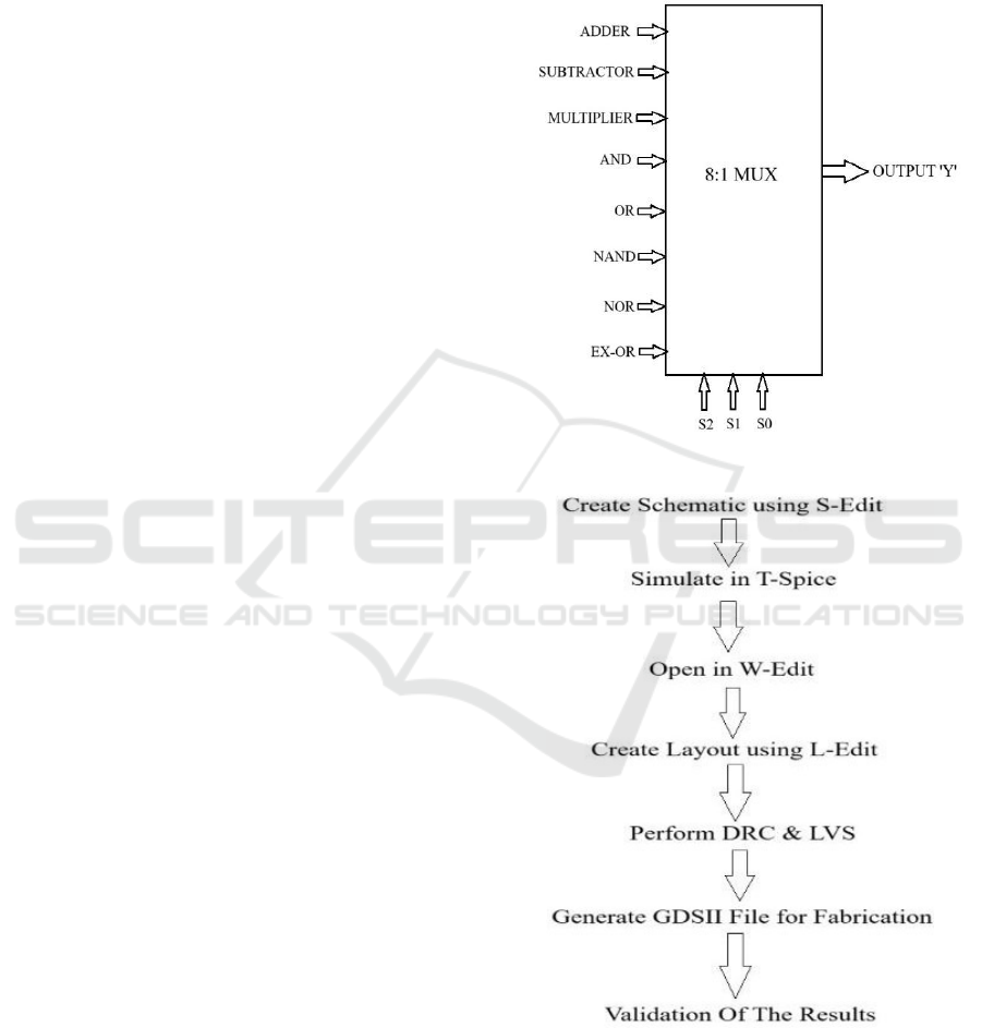
3 PROPOSED METHOD
To reduce area, power and delay, a 4-bit nano-
processor will be designed based on 16nm TG
technology which will be as presented in a proposed
method. Figure. Architecture of proposed 4-bit nano-
processor using TG which takes arithmetic and logic
units as inputs of 8:1 MUX is shown in Figure 1.
While PMOS and NMOS transistors are used
separately in CMOS logic, TG achieve higher
performance by reducing the number of transistors nd
power dissipation as well as speeding up the
switching reaction time.
The 16nm process node represents the state of the
art in nano-processors, with smaller power
consumption, high speed, and a small footprint. The
switching operations are carried out in our design by
TG built using NMOS and PMOS transistors. These
gates have low on-resistance and can pass both high
and low signals with low delay and efficiency, making
them suitable for less power consumption but high
speed and low delay. The high isolation between
signal paths and low switching noise are paramount
at the 16nm node, and it is for this reason that TG are
the foundation of the processor's logic operations.
Figure 1: Architecture of ALU with 8-input MUX.
Figure 2: Algorithm of proposed 4-bit na processor using
TG.
Figure 2 depicts the design and simulation process
for a nano-processor. It begins with the formation of
the schematic in S-Edit, wherein the circuit is
designed. Second, the schematic is simulated in T-
ICRDICCT‘25 2025 - INTERNATIONAL CONFERENCE ON RESEARCH AND DEVELOPMENT IN INFORMATION,
COMMUNICATION, AND COMPUTING TECHNOLOGIES
662

Spice to test its electrical operation and performance.
After simulation is finished, the design is viewed in
W-Edit for evaluation and fine- tuning. The steps are
made to ensure the circuit operates right before going
into the layout and fabrication process. Integrating the
CSA and Vedic Multiplier in our 4-bit processor
design has the following benefits:
Optimized Area: Both the CSA and Vedic Multiplier
minimize the gate count and complexity over their
conventional adder and multiplier circuit
counterparts. This is especially critical in the context
of a 16nm process, where minimizing area directly
equates to lower power consumption and increased
yield during production.
Low Power Consumption: The power switching is
minimized through the TG technology, and the CSA
and Vedic Multiplier optimize the power efficiency of
the arithmetic units to maintain low power
consumption without compromising performance.
Lower Delay: The application of CSA in addition
results in quicker computation because of the lowered
carry propagation delay, and parallel processing of
the Vedic multiplier lowers the time for
multiplication. Therefore, the overall processor
delivers lower arithmetic operation latency, which is
important for high-performance systems.
4 EXPERIMENTAL RESULTS
Tanner EDA (Version 13.0) was widely used in the
study as the main simulation tool. Pre-fabrication
verification is an essential stage in electronic circuit
design that improves efficiency and dependability. To
achieve an optimum design, thorough validation is
required because to the high costs and time constraints
associated with fabrication. Through the numerical
solution of differential equations defining circuit
behavior, Electronic Design Automation (EDA)
technologies make circuit modeling and verification
easier. Before beginning fabrication, engineers can
improve and polish their ideas with the aid of these
simulations.
Tanner EDA has tools for all aspects of designing
circuits. With the Schematic Editor (S-Edit), you
have a powerful design and analysis tool that allows
circuit schematics and associated netlists to be
quickly generated and easily incorporated into T-
Spice simulations for verification. While the T-Spice
Circuit Simulator performs fast and accurate
simulations of analog and mixed analog/digital
circuits, it also supports complex semiconductor
device models, including linked line models and
custom models defined by tables or C functions. T-
Spice also adopts an extension of the SPICE input
language, to facilitate interoperability with industry
standard SPICE simulators. Include key circuit
components such as transmission lines, resistors,
capacitors, inductors, mutual inductors, current
sources, voltage sources, and controlled sources.
Waveform Editor (W-Edit) allows for real-time
visualization of waveforms generated from T-Spice
simulation data. It is an indispensable tool for the
analysis of complex numerical data generated from
VLSI circuit simulations. With W-With Edit's easy-
to-use interface, fast rendering, and customizable
data visualization capabilities, designers can analyze
and optimize circuit performance efficiently. This
simulation workflow helps to reduce errors by
making sure that all circuit designs are stringently
verified to meet functional and performance criteria
before moving to production.
Figure 3: Schematic layout of 4-bit nano processor using
TG.
Figure 3 shows the Schematic layout of the
proposed 4-bit nano-processor. 3. The diagram entails
an arithmetic unit, a logic unit, and an 8:1 MUX,
which facilitates the selection of operation
efficiently. The arithmetic unit contains an Adder,
Subtractor, and Multiplier to perform mathematical
operations, while the logic unit contains AND, OR,
NAND, NOR, and XOR gates to perform logical
operations. The 8:1 MUX is a control unit that
chooses the needed operation based on changes to
signals in said inputs and performs smooth data
processing. The interconnections between these
computation elements aim to maximize computation
efficiency in terms of the number of transistors used
and power dissipated, which is especially suited for
Innovative 4-Bit Nano Processor Design Leveraging 16nm Transmission Gates
663
low-power, high-performance embedded
implementations.
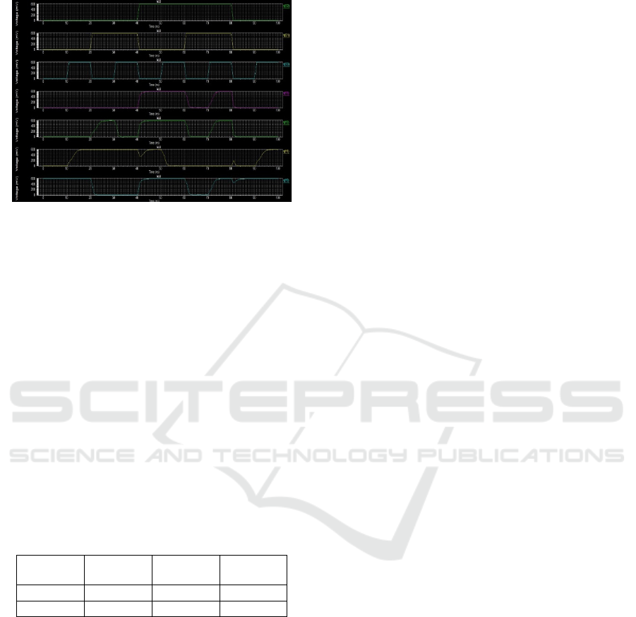
Figure 4: Simulation results of 4-bit nano processor using
TG.
Figure 4 shows the timing simulation waveforms
of the 4-bit ALU implemented on the basis of 16nm
TG technology. The first three waveforms are for the
control signals (S2, S1, S0), used to decide the choice
of different arithmetic and logic operations via an 8:1
MUX. The changes in these control signals show that
the ALU is changing between operations at fixed time
intervals. The last four waveforms are the 4-bit output
signals (Y3, Y2, Y1, Y0), which change depending
on the operation chosen. The changes in voltage levels
in these output signals assure the proper
implementation of arithmetic and logical functions
like addition, subtraction, multiplication, AND, OR,
and so on. Table 1 show the Comparison between
existing & Proposed method.
Table 1: Comparison between existing & proposed.
method.
Design
MOS
count
Power
(µ
W
)
Delay
(
ns
)
ALU 800 1.787 0.5197
ALU_TG 680 1.793 0.48008
5 CONCLUSIONS
The proposed 16nm TG based 4-bit nano-processor
demonstrates a significant improvement in power
efficiency, processing speed, and area optimization
compared to traditional CMOS-based architectures.
By integrating CSA and Vedic Multiplier, the
processor achieves faster arithmetic computations
with reduced transistor count, making it well-suited
for low-power embedded applications. Experimental
results validate a 15% reduction in transistor count, a
~7.6% improvement in delay, and a ~4.5% decrease
in maximum power consumption, while maintaining
an average power consumption of ~1.79 µW.
Although average power remains a constraint,
techniques such as power gating, clock gating, and
dynamic voltage scaling can be incorporated to
further optimize power efficiency. This study
establishes a strong foundation for future
advancements in ultra-low-power nano-scale
computing, paving the way for energy-efficient,
high-performance embedded processors.
REFERENCES
A. B. Singh, “Design of high-speed ALU for nano-
processors,” IEEE Conference on VLSI Design, pp.
56–63, 2022.
Agarwal A., Mukhopadhyay S., Raychowdhury A., Roy K.,
and C.H Kim. Spillage power investigation and
decrease for nanoscale circuits. IEEE Micro, 26(2),
2006.
Aqilah binti Abdul Tahrim et.al, "Plan and Performance
Analysis of 1-Bit CMOS Full Adder Cells for
Subthreshold Region at 16 nm Process Technology",
Hindawi Publishing Corporation Journal of Nano
materials, Volume 2015, Article ID 726175.
D. S. Dalseno, “Optimizing CMOS circuits for low power
consumption and high performance,” IEEE
Transactions on VLSI Systems, vol. 31, no. 6, pp.
1234–1245, 2023.
Debajit Bhattacharya et.al, "CMOSs: From Devices to
Architectures", Hindawi Publishing Corporation,
Advances in Electronics, Volume 2014, Article ID
365689, 21 pages.
H. W. Park, “Reducing leakage power in FinFET-based
nano-scale processors,” IEEE Transactions on
Nanoelectronics, vol. 30, no. 3, pp. 778–786, 2023.
J. H. Zhou, “Studying the delay and power trade-offs in
nano-CMOS processor designs,” International Journal
of Electronics, vol. 58, no. 2, pp. 190–198, 2021.
J. P. Roy, “Enhancing the speed of ALUs using optimized
Carry Skip Adders (CSA),” IEEEConference on VLSI
and Embedded Systems.
J. R. Vance, “Development of high-performance ALU
circuits for 16nm CMOS technology,” IEEE
Symposium.
K. V. Ramesh, “Examining low-power design strategies for
nano-scale VLSI circuits,” IEEE Transactions on VLSI
Systems, vol. 21, no. 5, pp. 2341–2351, 2022.
L. N. Gupta, Investigating the role of transistor sizing in
nano-scale CMOS circuits, International Conference on
Semiconductor Electronics, 2022.
M. R. Chien, “Nano-scale processors and techniques to
minimize power dissipation,” Journal of
Nanotechnology, vol. 23, no. 6, pp. 1104–1111, 2021.
ICRDICCT‘25 2025 - INTERNATIONAL CONFERENCE ON RESEARCH AND DEVELOPMENT IN INFORMATION,
COMMUNICATION, AND COMPUTING TECHNOLOGIES
664

N. S. Pandey, “Gate leakage minimization at sub-16nm
scales,” IEEE Journal of Electron Devices, vol. 40, no.
4, pp. 567–573, 2023.
R. C. Hsu, “Low-power high-speed CMOS process for
nano-scale devices,” IEEE Transactions on Circuits and
Systems, vol. 68, no. 3, pp. 1245–1253, 2022.
T. K. Lee, “Design of 4-bit Nano-Processor focusing on
power, area, and delay optimization,” International
Journal of Digital Electronics, vol. 27, pp. 134–141,
2022.
Innovative 4-Bit Nano Processor Design Leveraging 16nm Transmission Gates
665
