
Graphene Based Microstrip Patch Antenna for Wireless
Communication Applications
R. Selvaraj, P. T. Kalaivaani, B. Lakshmipriya, M. Monisha, G. Sasirekha and L. Sindhumathi
Department of Electronics and Communication Engineering, Vivekanandha College of Engineering for Women, Namakkal,
Tamil Nadu, India
Keywords: Graphene Substrate, Microstrip Patch Antenna, ADS Software, Wireless Communication.
Abstract: This paper discusses a design and simulation of a microstrip patch antenna using graphene based dielectric
substrate for the advanced wireless communication application. Such an antenna is beneficial in terms of
miniaturization, bandwidth and efficiency compared to other conventional antennas used in some of the early
heart monitoring implantable devices. Graphene (εr=2.8, high thermal conductivity of ( ̃3000 W/m•K) and
low loss tangent (tanδ) greatly improves the antenna bandwidth (BW), efficiency and miniaturization. The
designed antenna is simulated in ADS the software with a wide frequency range from 1GHz to 10GHz with
frequency gap 0.05GHz. The performance parameters as return loss (S11), VSWR, gain, directivity are
studied. The results show that the return loss is low so as to have a good impedance matching and the improved
radiation patterns make graphene-based antenna be potential applications in future high-frequency and next-
generation wireless communication systems.
1 INTRODUCTION
The recent progress of wireless communication
technology has required the antennas of high
performance that can satisfy the requirements of the
modern wireless communication systems. In the
family of antennas, microstrip patch antennas have
been of great interest, because of their low profile,
light weight and simplicity of integration with other
electronics. These antennas are commonly used for
mobile communications, satellite communications
and radars. The materials properties are of very
important aspects for the optimization and designing
of microstrip patch antennas. The conventional
dielectric materials (FR4 and rogers) have been well
researched and used in antenna applications.
However, with the introduction of new materials like
graphene there are new opportunities to improve the
performance of microstrip patch antenna. Zhang, Y,
et al., 2024 Graphene, a monolayer of carbon atoms
in a 2D hexagonal lattice, shows extraordinary
characteristics like high thermal conductivity,
mechanical strength and its excellent electrical
conductivity. These properties render graphene to be
an appealing material for demonstrating microstrip
patch antennas.
Graphene's exceptional properties may improve
the optimal performance of antenna. With large
dielectric constant (εr = 2.8), the decomposition
temperature of 471 °C, and the low dissipation factor
(tanδ, 0.002 at 1 GHz), the LTO can be used for high-
frequency applications with effective signal delivery
and reduced energy wastage Zhang, Y, et al., 2024.
Moreover, the extraordinary thermal conductance of
graphene (~3000 W/m•K) guarantees effective heat
removal, which is important to preserve
performance, in particular in high frequency regime
4.
In this paper, the microstrip patch antenna is
designed and simulated with a graphene based
dielectric material for future wireless communication
generation. The designed antenna is simulated with
the ADS (Advanced Design System) software
between a frequency range of 1 GHz- 10 GHz (step
frequency is 0.05 GHz). The performance
parameters; S11 return loss, VSWR, gain, and
directivity are studied for assessing the proposed
graphene based antenna.
504
Selvaraj, R., Kalaivaani, P. T., Lakshmipriya, B., Monisha, M., Sasirekha, G. and Sindhumathi, L.
Graphene Based Microstrip Patch Antenna for Wireless Communication Applications.
DOI: 10.5220/0013900700004919
Paper published under CC license (CC BY-NC-ND 4.0)
In Proceedings of the 1st International Conference on Research and Development in Information, Communication, and Computing Technologies (ICRDICCT‘25 2025) - Volume 3, pages
504-510
ISBN: 978-989-758-777-1
Proceedings Copyright © 2025 by SCITEPRESS – Science and Technology Publications, Lda.

2 ANALYSIS AND DESIGN
2.1 Graphene as a Substrate
Chen, H., et al., 2024 Graphene is an excellent choice
for microstrip patch antenna substrates due to its
unique electrical and mechanical properties. Its
tunable conductivity allows frequency
reconfiguration, making it suitable for multi-band
applications. The high electrical conductivity and low
loss characteristics improve antenna efficiency,
especially for high-frequency communications.
Graphene enables antenna miniaturization while
maintaining high performance, essential for compact
and wearable devices. Its superior bandwidth and
gain enhance data transmission capabilities in
advanced networks like 5G and terahertz
communications. The lightweight and flexible nature
of graphene allows the development of bendable
antennas for flexible electronics and aerospace
applications. Its exceptional thermal conductivity
ensures efficient heat dissipation, maintaining stable
antenna. Graphene-based substrates integrate well
with nanotechnology, supporting innovations in IoT
and smart sensing applications. The material’s ability
to reduce signal attenuation enhances overall antenna
radiation efficiency. With these advantages, graphene
is paving the way for the future of high-performance
communication systems
2.2 Conductivity of Graphene
Graphene's conductivity is highly dispersive and can
be tuned to behave like a metal or a semiconductor.
Graphene is structurally an ultrathin layer of carbon
atoms that forms a honeycomb lattice, sandwiched
between two different media. The surface
conductivity of it depends on some parameters, such
as the angular frequency (ω), chemical potential (µc),
scattering rate (Γ) and temperature (T). Conductivity
of graphene’s s(Z) fits a Kubo formula (differently for
intra- and inter-band), namely: (1,5).
The intraband conduction in graphene is mainly
attributed to free carrier transport and is dominant for
low frequencies. It depends on chemical potential,
temperature etc, and can be calculated
mathematically as:
𝜎
= − 𝑗
(/𝒯)
+ 2𝑙𝑛
(
𝑒
/
+ 1
)
(1)
𝜎
=−𝑗
𝑙𝑛
(
)
(
)
(2)
where K
B
is the Boltzmann constant, h the
Planck’s constant, e the electron charge, ω the angular
frequency, Γ the scattering rate, T the temperature,
and μ
c
the chemical potential.
2.3 Patch Antenna Design with ADS
The width w, of the microstrip patch antenna was
obtained from Equation (3)
𝑤=
(3)
where f
o
= operation frequency, c = speed of light,
ε
r
= dielectric constant of the substrate. In order to
determine the length of the patch, L, we need to
perform a few additional computations.It is necessary
to start by figuring out the dielectric constant. In
Equation (4), we may find the dielectric constant of
the substrate.
𝜀
=
+
1+ 12
(4)
where h = thickness of the substrate, ε
eff
= effective
dielectric constant of the substrate. The value for
effective length can be calculated by using Equation
(5):
𝐿
=
(5)
The following step is to compute the length
extension, which is denoted by ∆L. Because of
fringing effects, the microstrip antenna gives the
impression of being far bigger electrically than its real
physical dimensions. Equation (6), which gives the
length extension, is as follows:
∆𝐿 = 0.412 ×
.
.
.
.
(6)
The actual length of the patch, L, is obtained by
Equation (7):
𝐿=𝐿
− 2∆𝐿 (7)
In order for patch antennas to function properly,
the design process must begin with a finite ground
plane. Equations (8) and (9) can be used to determine
the length and width of the ground plane,
respectively.
𝐿
=6ℎ+𝐿 (8)
Graphene Based Microstrip Patch Antenna for Wireless Communication Applications
505
𝑊
=6ℎ+𝑤 (9)
where w = width of the patch antenna, L = length of
the patch antenna, W
g
= width of ground plane. L
g
=
length of ground plane C. A. Balanis, 2016.
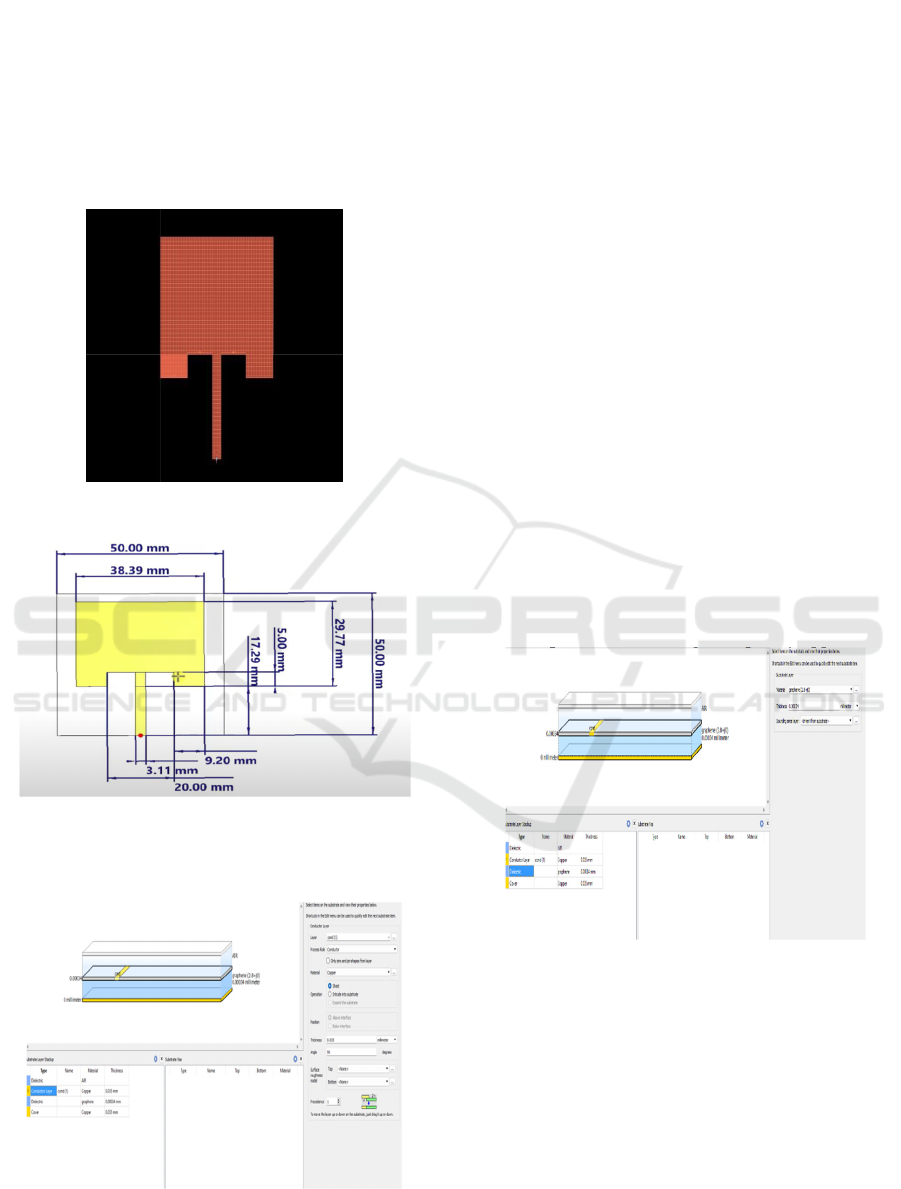
The figure 1 and 2. Shown below are the layout
design and dimensions of the Microstrip patch
antenna for the chosen substrate, rectangular patch
and the ground plan.
Figure 1: Layout design of microstrip patch antenna.
Figure 2: Dimensions of the microstrip patch antenna.
2.4 Conductor Layer Selection
Figure 3: Conductor layer selection.
The above figure 3 shows the conductor layer
selection in Advanced Design System (ADS) for
designing a microstrip patch antenna. In this setup,
copper is chosen as the conducting material with a
thickness of 0.035 mm. This layer forms the radiating
patch of the antenna, which is essential for
transmitting and receiving electromagnetic waves.
The settings panel on the right allows the user to
define the conductor's material, thickness, and
positioning within the substrate. The substrate layer
stackup displayed at the bottom shows multiple
layers, including air (dielectric), copper (conductor),
graphene (dielectric), and another copper layer
(cover), establishing the fundamental structure of the
antenna.
2.5 Dielectric Layer Selection:
Graphene Substrate
The image shown below focuses on the dielectric
layer selection, where graphene is used as the
substrate material. The thickness of this dielectric
layer is 0.00034 mm (0.34 µm), Faruk et.al, 2021;
Mollah, et al, 2021 making it extremely thin
compared to conventional substrates. Graphene is
selected due to its exceptional electrical and
mechanical properties, which can enhance the
antenna's performance in high-frequency applications
Figure 4: Dielectric substrate selection.
In figure 4, The settings panel on the right displays
options for adjusting the dielectric layer’s material
and thickness, ensuring proper electromagnetic wave
propagation. The substrate layer stackup at the
bottom shows the arrangement of layers, with
graphene serving as the dielectric medium between
the top copper patch and bottom copper ground plane.
ICRDICCT‘25 2025 - INTERNATIONAL CONFERENCE ON RESEARCH AND DEVELOPMENT IN INFORMATION,
COMMUNICATION, AND COMPUTING TECHNOLOGIES
506
2.6 Cover Layer Selection: Ground
Plane
Figure 5: Cover layer selection.
The protective shielding layer is made of 0.035 mm
thick copper as shown in figure 5. This cover is
important to protect the antenna structure against
extraneous influences and environmental impact.
Furthermore, copper is a conductive material
allowing it to shield unwanted RF radiation and
maintain signal fidelity. With little external
perturbation, the shielding layer can improve the
performance and stability of the antenna system
Faruk et.al, 2021.
2.7 Design Parameters and
Configurations
Here is a well-structured table for the given
parameters and values:
Table 1: Design Parameters.
Parameter Value
Real Permittivity (ε
r
Real) 2.8
Imaginary Permittivity (ε
r
Imaginary) 0
Loss tangent (tanδ) 0.002
Real Permeability(μ
r
) 1
Imaginary Permeability(μ
r
) 0
Frequency (TanD) 1GHz
Step size 0.01GHz
Upper range 10GHz
Conductivity 3000W/m.k
Z conductivity ~10W/m.k
Heat capacity(Cv) ~0.7J/g.K
Patch Antenna dimensions As per fig.2
For the analysis the frequency plan setup was also
described with the important parameters for the
evaluation of the antenna performance. A linear
sweep frequency from 1 to 10 GHz was used. The
steps were set to 181 for the sweep, which means a
resolution step of 0.05GHz. When a checkmark was
checked in the box, the frequency plan was on. Such
configuration permitted accurate measurements over
the large frequency bandwidth, providing the
required number of points for an optimal analysis and
modeling of the antenna performance in the
considered MegaHetz span.
The above table 1 shows the design parameters for
the graphene-based microstrip patch antenna are
carefully selected to optimize its performance. The
permittivity (εr) is set at 2.8 with an imaginary value
of 0, ensuring minimal dielectric losses, while the loss
tangent (tanδ) of 0.0001 further confirms very low
energy dissipation. Since graphene is non-magnetic,
the permeability (µr, Real) is 1, and the imaginary
permeability (µr, Imaginary) is 0, meaning it does not
influence the magnetic properties of the antenna. The
Djordjevic model parameters define the frequency-
dependent loss characteristics, with a TanD frequency
of 1 GHz, a low-frequency limit of 1 kHz, and a high-
frequency range extending up to 1 THz, making the
design suitable for a wide frequency spectrum.
In terms of thermal properties, graphene exhibits
an outstanding thermal conductivity of 3000 W/m·K,
which enables efficient heat dissipation, although its
Z-axis conductivity is lower at ~10 W/m·K, affecting
vertical heat transfer. The heat capacity (Cv) of
approximately 0.7 J/g·K indicates its capability to
store and release thermal energy efficiently.
Additionally, the ground plane is designed to be
larger than the patch to enhance radiation efficiency
and minimize substrate-induced losses, which helps
in achieving better antenna performance. These
design considerations ensure that the graphene-based
microstrip patch antenna operates effectively across a
broad frequency range while maintaining thermal
stability and minimal signal loss.
3 RESULTS ANALYSIS
The simulation results confirm that the graphene-
based microstrip patch antenna achieves excellent
impedance matching, with an S
11
return loss of
approximately -0.030 dB at 2.25 GHz, ensuring
minimal reflection and high efficiency.
Graphene Based Microstrip Patch Antenna for Wireless Communication Applications
507
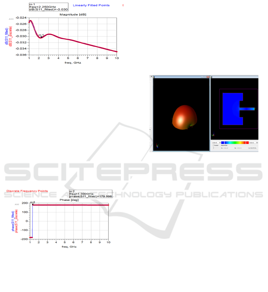
3.1 S11 Magnitude and Phase Response
Figure 6: Magnitude vs frequency.
In Figure 6, the S11 parameter (return loss) is an
important measure of how well the antenna is
matched to the feeding system. It is a value of
reflected power back due to impedance mismatch.
The graph demonstrates that at f = 2.25 GHz the
return loss is about -0.030 dB 1, meaning an almost
perfect impedance fit. Smaller S11 value results in
higher power transfer and less loss. The gradual
decrease at higher frequencies implies that the
antenna could work effectively in a wide bandwidth
range. We aim to design a G-GMSA for wireless
applications, and in such a desire, the low value of the
return loss at the desired frequency indicates superior
performance and less loss in the signal.
Figure 7: Plot of phase vs frequency.
In Figure 7, the phase of S
11
indicates the phase
shift of the reflected signal concerning the incident
signal. At 1.3 GHz, the phase is approximately 180°,
meaning that at this frequency, the reflected signal is
almost completely out of phase with the incident
signal Zhang, Y et al, 2024; Boopalan, et al, 2017.
The phase transition suggests that at lower
frequencies, the antenna exhibits significant phase
variations, which might affect the stability of signal
transmission. However, the relatively stable phase at
higher frequencies confirms a well-behaved
impedance response over the operating range. This
phase behavior aligns with the design goal of
achieving stable radiation characteristics, particularly
for applications requiring high efficiency and low
phase distortion.
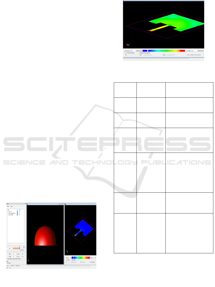
3.2 Radiation Pattern and Surface
Current Distribution 3D Analysis
The 3D visualization and field distribution shown in
Figure 8 provide a comprehensive view of the
electromagnetic field intensity across the antenna
structure.
Figure 8: Radiation and surface current distribution.
The image presents the radiation pattern and
surface current distribution of a microstrip patch
antenna with graphene as the substrate material. The
left side of the image illustrates the 3D radiation
pattern, which appears directional with an
asymmetrical distribution, indicating focused energy
radiation in a particular direction. The color intensity
represents the power density, with brighter regions
showing maximum radiation intensity.On the right
side, the current distribution is displayed using a color
scale, where blue represents minimal current flow and
red represents maximum current intensity. The
current is more evenly spread across the patch,
particularly near the feedline and patch edges,
suggesting moderate resonance behavior. This
configuration suggests that the antenna exhibits
directional gain, which can be beneficial for point-to-
point wireless communication applications.
This image also shows the radiation properties
and current distribution of the graphene based
microstrip patch antenna designed by ADS
software. On the lefthand side of the figure 9, a 3D
hemispherical radiation pattern is demonstrated that
is fairly rounder, implying wider coverage as well as
non-direc-tionality. Gradient of red to white color
shows the intensity of the radiation in which a
brighter area represent stronger radiation.
ICRDICCT‘25 2025 - INTERNATIONAL CONFERENCE ON RESEARCH AND DEVELOPMENT IN INFORMATION,
COMMUNICATION, AND COMPUTING TECHNOLOGIES
508
This picture shows the 3D radiation pattern for
the proposed MP-SA (viewed from the bottom). It
reveals the radiated energy out of the attached
antenna by displaying how the signal is traveling in
different directions A side view shows also the
distribution of the electric field at the feed point,
which represents how the energy is introduced into
the antenna structure. Such conclusion is important
to account for potential effect of graphene-based
substrate to improve the performance of the antenna.
On the left-hand side of the image, the distribution
of the radiation is shown and in the hemispherical it
becomes obvious that this pattern mimics the
directional emission of the electromagnetic waves.
This is colored black to green from high to low
radiation (red indicated the highest radiation
regions). The following right panel depicts the
surface current distribution on the patch which
illustrates the electric field variation in magnitude,
with overflow directions being blue shows minimum
current density, whereas lighter regions indicate a
high energy level. This visualization also leads to
interpretation of the antenna gain, efficiency and
directivity for wireless communication applications.
This figure.10below represents the final animated
simulation of the designed microstrip patch antenna,
showcasing the current distribution across the patch.
The color gradient indicates different current
intensity levels, with red denoting high current
concentration and blue representing minimal flow.
The feed line excitation is visible, ensuring proper
energy transfer to the patch. The analysis of current
distribution helps in optimizing antenna performance
by identifying areas of maximum radiation. This
visualization is crucial for evaluating impedance
matching and overall efficiency. Table 2 gives the
overall result summary.
Figure 9: Symmetrical radiation and localized current
distribution (front side view).
Figure 10: Animated simulated current distribution.
Table 2: Results summary.
Feature Graphene
based Design
Traditional Designs
(FR4, Rogers,
RT/Duroid5880)
Material Graphene
based
materials
FR4, Rogers,
RT/Duroid5880
Frequenc
y
1GHz to
10GHz
Specific bands such as
4.27GHz to 8.58GHz
for multiband desi
g
n
S
11
value -15.2dBi near
ideal
performance
very low
reflection
Varies depending on the
design often optimized
for specific frequencies
Performa
nce
Consistently
low S
11
values
suggests
efficient
operation
over wide
ran
g
e
Good performance over
specific frequency
bands but may not cover
wide range.
Gain Enhanced by
graphene’s
superior
properties,
Comparatively low
Impedanc
e
Matching
Excellent
impedance
matching at
2.250GHz
and
potentially
across wide
ran
g
e
Optimized for specific
frequencies with good
matching.
3.3 Advantages of Graphene-Based
Design over Traditional Designs
Wider frequency range – Graphene-based antennas
operate efficiently from 1 GHz to 10 GHz, whereas
Graphene Based Microstrip Patch Antenna for Wireless Communication Applications
509

traditional designs are usually optimized for specific
frequency.
Lower reflection (better S
11
performance) – The
S
11
value at 2.25 GHz is -0.030 dB, indicating almost
perfect impedance matching, which is better than
most traditional designs. Enhanced gain – Graphene’s
superior electrical properties contribute to higher gain
compared to some traditional materials.
Efficient impedance matching – Graphene-based
designs provide excellent impedance matching across
a broader frequency range.
4 CONCLUSION AND FUTURE
WORK
This research successfully designed and analyzed a
graphene-based microstrip patch antenna with
superior performance over conventional materials.
Graphene’s high electrical conductivity, low loss
tangent, and flexibility significantly enhanced
antenna efficiency, bandwidth, and radiation
characteristics. The simulation results demonstrated
improved impedance matching, reduced return loss,
and higher gain, making graphene-based MPAs ideal
for advanced wireless communication. The study
highlights graphene’s potential for applications in 5G,
IoT, satellite communication, and wearable devices.
Future research will focus on experimental validation,
hybrid material integration, and advanced fabrication
techniques. Long-term stability and environmental
impact studies are essential to ensure real-world
reliability. Overall, graphene-based antennas pave the
way for highly efficient, miniaturized, and high-
performance wireless communication systems.
The future scope of this project includes
experimental validation through fabrication and real-
world testing to compare simulated and measured
results. Exploring graphene synthesis techniques like
chemical vapor deposition and exfoliation can further
enhance antenna performance. Optimizing graphene
antennas for mmWave 5G, IoT, and reconfigurable
applications can improve efficiency and adaptability.
Integration with advanced materials like
metamaterials and nanocomposites can boost
performance. Flexible and wearable graphene
antennas may drive advancements in biomedical and
smart textiles, while energy-harvesting designs could
enable self-powered devices. Extending graphene
antennas into the terahertz range may support ultra-
fast communications and space applications.
Ensuring commercial viability through cost-effective
large-scale manufacturing and industry
collaborations can accelerate real-world adoption.
REFERENCES
A. K. Geim and K. S. Novoselov, “The rise of graphene,”
Nat.Mater., vol. 6, pp. 183–191, (2007).
Boopalan G, Ramakrishna V, Jayanth N V, “Analysis of
Graphene Based Planar Antennas for Terahertz
Application (2017)” IEEE Micro, Mar./Apr. (2017).
C. A. Balanis, Antenna Theory Analysis and Design,
3rdedition, John Wiley&sons,2016
Chen, H., Wang, J., & Xu, Y. "Performance Enhancement
of Microstrip Patch Antennas
Using Graphene Based Substrates." International Jour
nal of Microwave and WirelessTechnologies,16(3),
(2024)215-223.
D. Correas-Serrano and J. S. Gomez-Diaz, "Graphene-
based antennas for terahertz systems: A review," in
Proceedings of the 2015 IEEE International
Symposium on Antennas and Propagation &
USNC/URSI National Radio Science Meeting, (2015).
J. M. Jornet and I. F. Akyildiz, "Graphene-based
nano antennas for electromagnetic nanocommunicatio
ns in the terahertz band," in Proceedings of the Fourth
European Conference on Antennas and Propagation
(EuCAP), (2010).
Li, X., Zhao, Q., & Wu, T. (2023). "Graphene- Integrated
Microstrip Patch Antenna for Terahertz
Communication Systems." Journal of Infrared,
Millimeter, and Terahertz Waves, 44(7), 789-798.
M. S. H. Mollah, M. S. Hossain, and M. T. Islam, "Design
and performance improvement of microstrip patch
antenna using graphene material for communication
applications," in Proceedings of the 2021 IEEE
Symposium on Computer Applications & Industrial
Electronics (ISCAIE), 2021.
Mohammad Sarwar Hossain Mollah,Omar Faruk et.al,
“Design and Performance Improvement of Microstrip
patch Antenna Using Graphene Material for
Communication Applications”978-1-6654-0338-
2/21/$31.00 (2021) IEEE
Zhang, Y., Liu, S., & Li, Z. "Design and Analysis of a
Graphene-Based Microstrip Patch Antenna for 5G
Applications." IEEE Transactions on Antennas and
Propagation, 72(1), (2024) 45-53.
ICRDICCT‘25 2025 - INTERNATIONAL CONFERENCE ON RESEARCH AND DEVELOPMENT IN INFORMATION,
COMMUNICATION, AND COMPUTING TECHNOLOGIES
510
