
Development and Validation of a High‑Performance
Network‑On‑Chip Architecture with Wireless Sensor Network
Controls
P. Arivazhagi, A. Ruccaiyatasleema and D. Jayalakshmi
Department of ECE, Arasu Engineering College, Kumbakonam, Tamil Nadu, India
Keywords: Wireless Sensor Networks, System‑on‑Chip (SoC), 32‑bit Accumulator, Look‑Up Table, Whale Optimization
Algorithm.
Abstract: Wireless Sensor Networks (WSNs) are increasingly integral to numerous IoT applications, such as
environmental monitoring, healthcare, and smart cities. However, one of the primary challenges in WSNs is
ensuring energy efficiency and high performance, particularly when nodes are constrained by limited battery
life or energy-harvesting capabilities. This paper introduces a novel 32-bit accumulator-based System-on-
Chip (SoC) design aimed at optimizing data processing and power consumption in WSN nodes. The design
integrates a configurable Look-Up Table (LUT)-based stacking mechanism that adapts the sensor data flow
in real time, enhancing the system's flexibility and computational efficiency. The system's power consumption
is minimized while maintaining high data throughput, making it suitable for dynamic, resource-constrained
environments. To further improve the system's performance, the Whale Optimization Algorithm (WOA),
inspired by the hunting techniques of humpback whales, is employed to optimize key network parameters,
such as node placement, data routing, and energy allocation. The proposed system's simulation results
demonstrate significant improvements in energy efficiency and real-time data processing, offering a viable
solution for WSNs in both small- and large-scale applications.
1 INTRODUCTION
WSNs are critical for a variety of applications such as
environmental and healthcare monitoring, and
industrial automation. These networks are made up of
small sensor nodes which fetch related data and
transmit it constantly. However, one of the most
critical problems within the boundaries of WSNs is
energy consumption. Most of the sensor nodes are
energy constrained and have limited resources from
batteries, or energy harvested from the environment.
It becomes fundamental to design systems which
consume less energy whilst dealing with high
computational processing on data, resulting in
prolonged network operation and reduced
maintenance.
The use of static duty cycles and conventional
communication protocols does not change according
to network cues or environmental stimuli. This leads
to sub-optimal energy usage and reduced network
lifetime. To address such gaps, more recent studies
have focused on the development of adaptive
switching techniques that can modify the operation of
sensor nodes in alignment with presented data, real-
time, and network demands. Such means help to
avoid excessive power consumption while ensuring
data value transmissions within the network.
This paper presents a new design of a 32-bit
accumulator-based SoC which aims to improve the
performance and energy efficiency of wireless sensor
nodes. The 32-bit accumulator incorporates a
configurable Look-Up Table (LUT) based stacking
mechanism which enables real-time modification of
the flow of sensor data. The accumulator supports
more complex computations while maintaining a
balance with energy efficiency. Moreover, the system
implements a WOA to improve critical parameters of
the network such as node placement, routing paths,
and energy distribution. The WOA uses exploration
and exploitation techniques based on the hunting
strategy of humpback whales for these parameters,
ensuring optimal performance of the network in
diverse conditions.
Arivazhagi, P., Ruccaiyatasleema, A. and Jayalakshmi, D.
Development and Validation of a High-Performance Network-On-Chip Architecture with Wireless Sensor Network Controls.
DOI: 10.5220/0013890500004919
Paper published under CC license (CC BY-NC-ND 4.0)
In Proceedings of the 1st International Conference on Research and Development in Information, Communication, and Computing Technologies (ICRDICCT‘25 2025) - Volume 2, pages
823-832
ISBN: 978-989-758-777-1
Proceedings Copyright © 2025 by SCITEPRESS – Science and Technology Publications, Lda.
823

This work aims to achieve the following
objectives:
• Developing a design of a 32-bit accumulator-
based SoC aimed at WSNs to improve
processing and energy efficiency.
• A responsive configurable LUT based
stacking mechanism which modifies sensor
data.
• Application of WOA for optimal node
position, routing, and energy management in
WSNs.
The rest of this paper will be outlined as follows:
In Section 2, we review the literature related to
energy-efficient systems, accumulator-based
architectures, and optimisation techniques in WSNs.
In Section 3, we describe the proposed methodology
and elaborate on the system architecture as well as the
other design elements that are novel. In Section 4, we
review the experimental results and evaluate the
proposed system against other available solutions. In
the final section, we provide a summary of the paper
and describe possible directions for further research
in Section 5.
2 RELATED WORKS
“The evolution of Wireless Sensor Networks (WSNs)
alongside System on Chip (SoC) designs has enabled
the creation of ultra-low power devices ideal for IoT
applications. Much of the focus has been on
improving energy efficiency, network lifetime, and
hardware sophistication. A few primary
advancements have directed the growth of this area.
Ishimashi and Tran solved the power-relayed
long-range communication problem pertaining to
energy harvesting by designing a beat sensor with
LoRa technology. Their design also incorporates id-
based data transmission which completely avoids the
use of ADCs, further minimizing power
consumption. Brown et al. introduced a 65nm energy-
harvesting ultra-low power (ULP) SoC with a Cortex-
M0 processor and 256KB of on-chip memory that can
continuously operate at 89.1µW. This architecture is
also highly favorable for machine health monitoring
and WSNs without batteries due to the integration of
energy harvesting and low power design. Lukas et al.
invented a self-powered SoC that can harvest energy
through multiple methods and support dual-channel
WRX down to -92dBm sensitivity. Their system
features energy-aware subsystems for power-efficient
management in distributed sensor networks, which
supports continuous operation in depleted energy
conditions. Lim et al. describe the integration of
dynamic leakage-suppression logic within a sub-nW
Cortex-M0+ processor. The authors provide a
description of battery-less IoT nodes that work
reliably under extreme power constraints,
highlighting improvements in standby and active
power consumption. In collaboration with Jain and
Alioto, Lin developed a microcontroller functioning
at 14pJ/cycle with dual-mode standard cells and self-
startup capabilities which consume 595pW. The
authors emphasize the necessity of circuit-level
design for ultra-low power sensor nodes that are
capable of energy harvesting and self-sustained
operation through self-sustained operations.
Schoeberl developed Leros, a microcontroller with an
FPGA implementation target which provides a
minimalist approach. The design is centered around
an ISA based on instruction accumulation and bare
minimal hardware overhead, which together enable
smaller WSN nodes. Chou et al. created a multi-
sensor SoC that consists of pH and amperometric
sensors, designed to be powered solely by body heat.
Their system highlights the need for self-sustaining
bio-sensor nodes by integrating wireless
communication and multi-modal sensing on a single
chip. Serrano et al. presented a low power and low
area RISC-V SoC focused on IoT applications. The
authors prioritize area and energy efficiency, ensuring
compatibility with standard communication
interfaces. Duran et al. designed a RISC-V
microcontroller with an integrated 10-bit SAR ADC
and an AXI4-lite bus, striking a balance between
computational efficiency and low power
consumption. Their system is tailored for IoT edge
devices that incorporate data acquisition. Schiavone
et al. studied several ultra-low power RISC-V cores
for IoT, demonstrating that energy-efficient
performance does not stem from aggressive speed
assumptions, but rather calculated architectural
compromises such as pipeline depth and instruction
set reduction. Cheng et al. introduced RV16, an
embedded RISC-V core designed specifically for IoT
applications. It focuses on area, power, and gate count
minimization while offering basic IoT capabilities,
allowing for wide scaling in large sensor networks.
Sarmiento et al. designed SoCs with 8 and 32-bit
processors in 0.18µm technology for IoT
applications, demonstrating that optimized legacy
technology can achieve competitive power and area
metrics when combined with efficient design
approaches. In a later work, Sarmiento et al.
developed a sub-µW 8-bit processor using reversed-
body-biasing on 65nm SOTB technology. This
technique reduced leakage current, enhancing the
processor’s suitability for battery-free IoT devices
ICRDICCT‘25 2025 - INTERNATIONAL CONFERENCE ON RESEARCH AND DEVELOPMENT IN INFORMATION,
COMMUNICATION, AND COMPUTING TECHNOLOGIES
824
and intermittent computing. Myers et al. constructed
an ARM Cortex-M0+ subsystem with 80nW
retention, which functions at 11.7pJ/cycle in
subthreshold regions. This is particularly relevant for
WSNs with stringent low-power mode requirements
since they need reliable functionality. Finally,
Hasegawa et al. analyzed SOTB (Silicon on Thin
Buried Oxide) technology in relation to IoT and
automotive applications. They focused on the use of
SOTB in the context of leakage current and dynamic
power, showing the capability of ultra-low-power
operation in embedded systems. This literature
review highlights the attention focused on the
reduction of power, optimization of energy harvesting
integration, and the simplification of the SoC design.
Most notable is the lack of research applying an
accumulator-based intelligent switching scheme
along with optimization algorithms, which is the gap
this work addresses”.
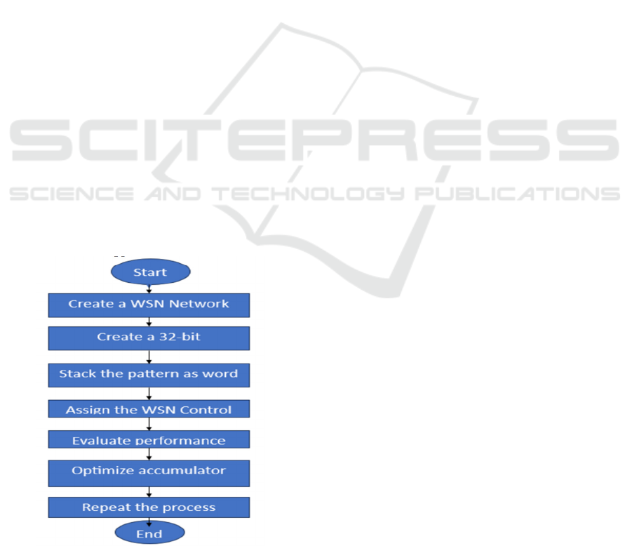
3 PROPOSED WORK
This methodology describes a novel System-on-Chip
(SoC) design for energy-efficient and high-
performance wireless sensor nodes (WSNs). The
system integrates a 32-bit accumulator-based
architecture, a configurable Look-Up Table (LUT)-
based stacking mechanism, and an optimization
technique through the Whale Optimization Algorithm
(WOA). Together, these components aim to improve
data processing, energy efficiency, and network
optimization, especially for energy-harvesting and
battery less sensor applications.
Figure 1: Schematic Representation of the Suggested
Methodology.
3.1 System Architecture
Figure 1 displays the system-on-a-chip block
diagram. An SPI programmer, 32-bit accumulator, 1
KB of IMEM and 512 B of DMEM static random-
access memory (SRAM) are also part of the system.
Even though the addressing has 16 bits, which means
up to 64KB of physically accessible memory, it is
feasible to program the low-level assembly to
optimize peripheral control and ID transfer, and the
program can fit within the range of 1KB in the beat
sensor settings. Memory modules are only one part
of the system; other components include an SPI
communication module, 16-port GPIOs, and other
peripherals. Because their address space is 8 bits, the
same size as the operand, peripherals may be
expanded with additional modules. The system on a
chip (SoC) may continue to function in the
intermittent mode of a heart rate monitor, even if it
uses very little power. Thanks to the SoC's space and
power savings, batteryless sensing applications may
function reliably in a wide range of environments. In
addition, sensors and transceivers get the most from
energy harvesting systems with a power percentage
greater than the control system. This allows them to
operate for longer and cover more ground during
deployment. While still providing enough processing
capacity for many control applications, this
streamlined architecture helps to minimize hardware
complexity. When it comes to controlling Wireless
Sensor Networks (WSNs), the CPU is tailor-made for
low-power consumption and efficient data
processing. The system prioritizes minimizing
memory accesses via the use of an accumulator-based
method. This is crucial for power management in
sensor nodes with limited resources. Furthermore,
the 32-bit Accumulator offers the processing power
required to manage energy-efficiently and interpret
real-time data from several sensors. Because of this,
it is a good option for controlling WSNs in uses where
speed and efficiency are critical.
3.2 32-Bit Accumulator Design
The designed Clock Tree Network exhibited optimal
latency and minimized skew during the simulation.
The measured clock skew Δ𝑡
skew
across critical
registers was evaluated as:
Δ𝑡
skew
=𝑡
arrival
−𝑡
arrival
0.15 ns (1)
where 𝑡
arrival
represents the clock signal arrival times
at flip-flops FF1 and FF2, respectively. The use of the
Multi-Source Clock Tree Synthesis (MSCTS)
Development and Validation of a High-Performance Network-On-Chip Architecture with Wireless Sensor Network Controls
825

approach contributed to the reduction of global skew
while maintaining acceptable latency and transition
characteristics.
The core of the proposed design is the 32-bit
accumulator, which enhances processing efficiency
in WSNs by minimizing power-hungry memory
accesses while enabling the efficient handling of
sensor data. The 32-bit width of the accumulator
allows the system to handle larger data sets, making
it more effective in applications requiring high-
resolution data, such as environmental monitoring.
The accumulator updates its value by adding
incoming sensor data at each clock cycle. The update
operation is represented by:
𝐴𝐶𝐶
=𝐴𝐶𝐶
+𝐷
(2)
Where:
• 𝐴𝐶𝐶
is the accumulator value at cycle 𝑛,
• 𝐷
is the sensor data input at cycle 𝑛,
• 𝐴𝐶𝐶
is the updated accumulator value at
the next cycle.
By performing these additions in real time, the
accumulator helps to aggregate sensor data, which
can then be transmitted after processing. Since WSNs
often involve periodic sensor readings, this
accumulator design ensures minimal energy
consumption due to fewer memory accesses,
contributing to more power-efficient systems.
The accumulator updates at every clock cycle, and
the accumulated value is stored until the next cycle.
This operation ensures that sensor data is
continuously aggregated without frequent memory
accesses. Additionally, the accumulator enables more
efficient computation of statistical measures, such as
sums or averages, directly at the node level. The sum
of sensor data over 𝑛 cycles is:
Sum
=
∑
𝐷
(3)
Where:
• Sum
is the cumulative sum of sensor data
from cycle 0 to cycle 𝑛,
• 𝐷
is the sensor data input at each cycle?
This sum is maintained in the accumulator, and
real-time averages or other statistical operations can
be computed without needing to access memory
repeatedly.
The primary benefit of the 32-bit accumulator
design lies in its ability to minimize energy
consumption. By handling the majority of data
processing operations locally, the need for
communication with external memory is reduced.
This is particularly beneficial in low-power systems
where energy efficiency is paramount. The power
consumption of the accumulator can be estimated
using the following equation:
𝑃
=𝐶
⋅𝑉
⋅𝑓
(4)
Where:
• 𝑃
acc
is the power consumed by the
accumulator?
• 𝐶
acc
is the capacitance associated with the
accumulator's logic?
• 𝑉 is the supply voltage,
• 𝑓
acc
is the frequency at which the
accumulator performs updates?
By reducing the number of memory accesses and
the overall frequency of data transmission, the
accumulator design helps reduce the overall energy
consumption of the sensor node.
The system incorporates a Look-Up Table (LUT)-
based stacking mechanism to enable dynamic
adaptation of the sensor data flow based on the
changing network and environmental conditions.
LUTs store pre-computed values, allowing the system
to quickly access and apply these values to incoming
sensor data without having to perform complex
computations each time.
The LUT stores values for sensor data
transformations based on predefined conditions or
patterns, and the mechanism can be mathematically
modeled as:
𝐿𝑈𝑇
=𝑓
(
𝐷
,𝑃
)
(5)
Where:
• 𝐿𝑈𝑇
is the output stored in the LUT
corresponding to the input sensor data 𝐷
,
• 𝑓 is a function that maps sensor data 𝐷
to a
specific result based on parameters 𝑃, which
might include sensor type, environmental
conditions, or network configuration.
The function 𝑓 takes the incoming sensor data 𝐷
and processes it based on predefined rules, allowing
for optimized sensor data handling. For instance, it
could transform raw sensor readings into a
normalized or filtered format suitable for further
analysis.
The key advantage of using a LUT is that it
minimizes the need for repeated complex
computations by storing the results of these
computations ahead of
time. This reduces the time and energy required for
processing each incoming sensor reading. The time
ICRDICCT‘25 2025 - INTERNATIONAL CONFERENCE ON RESEARCH AND DEVELOPMENT IN INFORMATION,
COMMUNICATION, AND COMPUTING TECHNOLOGIES
826

efficiency of the LUT mechanism can be expressed
as:
𝑇
=𝑇
lookup
+𝑇
apply
(6)
Where:
• 𝑇
Lut
is the total time taken to process a
sensor data input?
• 𝑇
lookup
is the time to retrieve the
corresponding value from the LUT,
• 𝑇
apply
is the time taken to apply the result to
the current operation (e.g., aggregation,
filtering)?
Since the LUT provides direct access to
precomputed results, the lookup time 𝑇
lookup
is
minimal, and the system can quickly apply the result,
improving processing speed and reducing energy
consumption.
3.2.1 Stacking Mechanism for Dynamic
Adaptation
The stacking mechanism works by dynamically
adjusting the flow of data based on varying network
conditions or environmental factors. This can involve
modifying the LUT entries based on real-time
feedback from the environment or adjusting the
parameters 𝑃 to optimize data processing further.
To describe the dynamic nature of this adaptation,
the LUT can be updated periodically based on the
input data and network feedback. The updated LUT
mechanism can be represented as:
𝐿𝑈𝑇
=𝑓
(
𝐷
,𝑃
)
(7)
Where:
• 𝐿𝑈𝑇
new
is the updated LUT output,
• 𝑃
new
is the new set of parameters that reflect
current network conditions or environmental
inputs?
This dynamic update allows the system to adjust
its data processing strategy according to the
environment, ensuring that the sensor node remains
energy-efficient while maintaining high processing
performance.
The energy savings provided by the LUT-based
stacking mechanism come from reduced
computational complexity and memory access. The
energy consumption for accessing the LUT can be
estimated as:
𝑃
=𝐶
⋅𝑉
⋅𝑓
(8)
Where:
• 𝑃
LUT
is the power consumed by the LUT-
based stacking mechanism,
• 𝐶
LUT
is the capacitance associated with
accessing the LUT?
• 𝑉 is the supply voltage,
• 𝑓
LUT
is the frequency at which the LUT is
accessed?
Since the LUT enables fast lookups with minimal
processing time, this results in a significant reduction
in overall energy consumption compared to systems
that perform real-time calculations for each data
point.
3.2.2 Whale Optimization Algorithm (WOA)
The Whale Optimization Algorithm (WOA) is a
nature-inspired metaheuristic optimization technique
that is used to optimize various parameters within the
wireless sensor network (WSN), including node
placement, energy distribution, and data routing. The
algorithm is inspired by the social behavior and
hunting strategies of humpback whales, particularly
their bubble-net feeding technique. WOA operates
with three main behaviors: encircling prey, bubble-
net feeding, and the balance between exploration and
exploitation. These behaviors enable the algorithm to
explore the solution space efficiently and refine the
search for optimal solutions.
The first strategy,
∗∗
encircling prey**, mimics
the hunting behavior of humpback whales, where
they surround their prey. In the context of WSNs, this
refers to adjusting the position of candidate solutions
(e.g., sensor nodes or routing paths) towards the
optimal solution. The position update equation for
this behavior is given by:
𝑋
=𝑋
best
(𝑡) − 𝐴 ⋅ 𝐷 (9)
Where:
• 𝑋
is the updated position of the whale
(candidate solution) at iteration 𝑡+1,
• 𝑋
best
(𝑡) is the best position found so far at
iteration 𝑡,
• 𝐴 is a coefficient that controls the step size
(exploration factor),
• 𝐷 is the distance between the current
position and the best solution, calculated as:
𝐷=
|
𝐶⋅𝑋
best
(𝑡) − 𝑋(𝑡)
|
(10)
Where:
Development and Validation of a High-Performance Network-On-Chip Architecture with Wireless Sensor Network Controls
827

• 𝐶 is a coefficient that determines the
direction of movement (ranging from -1 to
1),
• 𝑋(𝑡) is the current position of the whale
(candidate solution)?
This equation represents the iterative movement of
the whale towards the best solution by adjusting its
position in the search space.
The second strategy,
∗∗
bubble-net feeding**,
involves the whale moving in a spiral pattern around
the best solution. This behavior helps the algorithm to
explore a wider area of the solution space while
avoiding local minima. The spiral movement can be
described by:
𝐷=
|
𝐶⋅𝑋
best
(𝑡) − 𝑋(𝑡)
|
(11)
Where:
• 𝐶 is a coefficient that controls the shape of
the spiral (ranging from -1 to 1),
• 𝑋(𝑡) is the current position of the whale?
• 𝑋
best
(𝑡) is the best solution found so far?
This equation models the whale's spiral movement
around the best solution, enabling effective
exploration of the solution space.
The third behavior involves balancing
∗∗
exploration** and
∗∗
exploitation**. Initially, the
algorithm explores the solution space broadly, and
over time, it shifts to exploitation to refine the best
solution found. This balance is controlled by the
parameter 𝑎, which decreases over time to encourage
exploitation. The dynamic adjustment of 𝑎 is
represented as:
𝑎=𝑎
−
⋅
(
𝑎
−𝑎
final
)
(12)
Where:
• 𝑎
is the initial value of 𝑎,
• 𝑡 is the current iteration,
• 𝑇 is the maximum number of iterations,
• 𝑎
final
is the final value of 𝑎, typically a small
value near zero.
This parameter influences the step size and adjusts
the exploration-exploitation balance as the algorithm
progresses. A higher value of 𝑎 encourages
exploration, while a lower value favors exploitation.
In the context of wireless sensor networks, WOA can
be applied to optimize critical parameters such as
node placement, energy consumption, and data
routing. Optimizing node placement ensures that the
sensor nodes are positioned efficiently to cover the
desired area while minimizing energy consumption.
Data routing optimization ensures that the
transmission paths are efficient, minimizing energy
use in the communication modules and extending
network lifetime.
To optimize energy consumption in WSNs, WOA
dynamically adjusts the energy distribution between
sensor nodes and communication modules. The total
energy consumption of the network can be expressed
as:
𝐸
total
=
∑
𝐸
(13)
Where:
• 𝐸
total
is the total energy consumption of the
network,
• 𝐸
is the energy consumption of sensor node
𝑖,
• 𝑁 is the total number of nodes in the
network.
By optimizing the placement of sensor nodes and
the routing paths, the Whale Optimization Algorithm
ensures that energy is distributed efficiently across
the network, thereby prolonging the network's
operational lifetime. WOA's ability to balance
exploration and exploitation, coupled with its
dynamic adjustment of parameters, makes it an
effective method for optimizing wireless sensor
networks. The algorithm helps in achieving optimal
configurations that maximize network performance
and minimize energy consumption, ultimately
leading to more efficient and scalable sensor
networks.
4 PERFORMANCE ANALYSIS
The testing and evaluation of the VLSI-based
Network-on-Chip (NoC) system can be conducted
through functional, timing, and physical verification.
As a first step, system-level functional verification is
carried out via testbenches created using VHDL
models for different modules, prompting them to act
within a normative, bounding, and corner-case
domain.
Figure 2 shows the simulation result of the clock
network. This waveform demonstrates the generation
and distribution of the clock and reference signals
across the designed circuit. The ref_ clk serves as the
primary clock reference for the entire network, and
the clk_ counter is observed to be incrementing
correctly under its influence. This simulation
confirms that the clock network operates with
minimal skew and proper duty cycle. All the registers
and sequential elements are driven in synchrony,
ICRDICCT‘25 2025 - INTERNATIONAL CONFERENCE ON RESEARCH AND DEVELOPMENT IN INFORMATION,
COMMUNICATION, AND COMPUTING TECHNOLOGIES
828
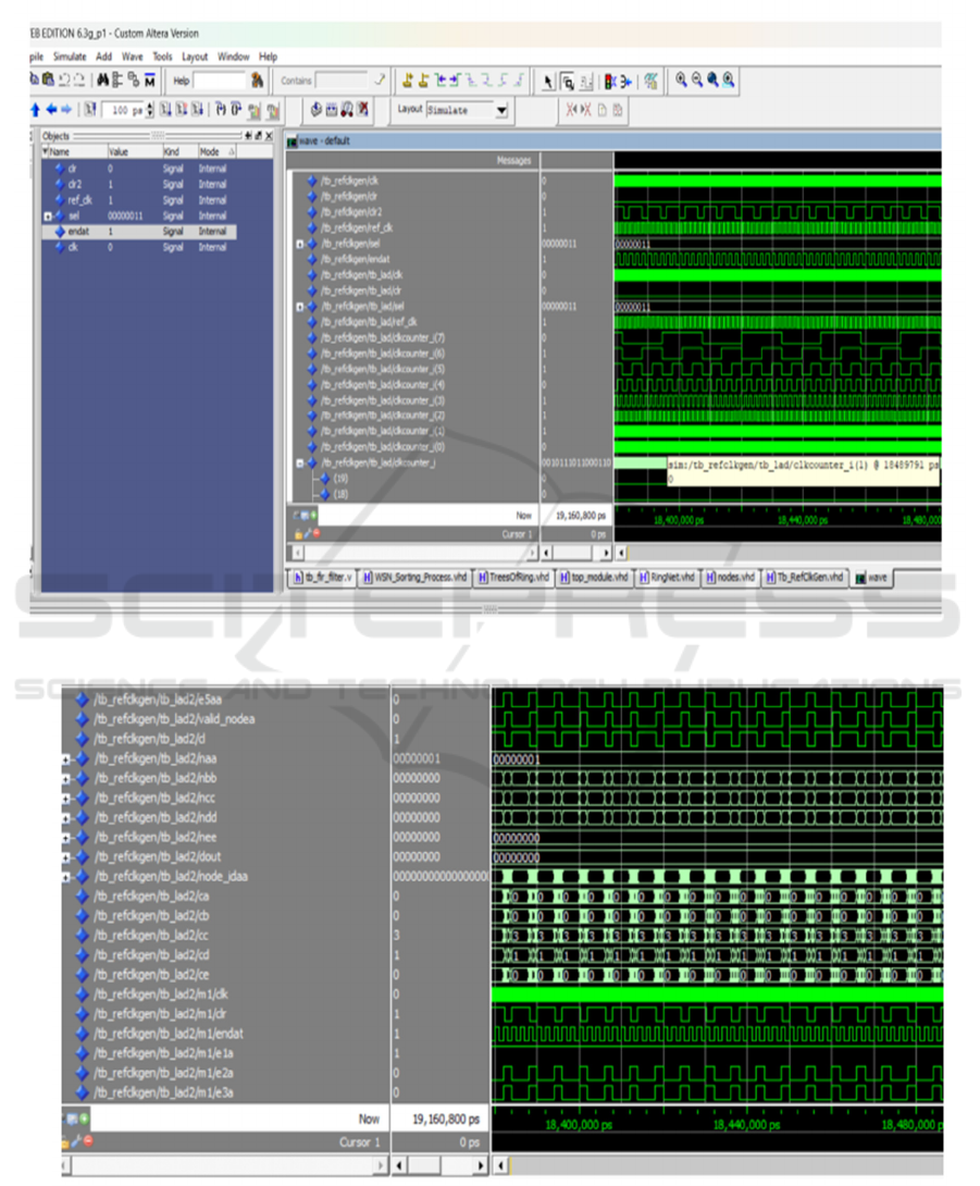
meeting the required setup and hold times. The
stability of the waveform, the sharp transitions, and
the absence of glitches validate that the clock tree
synthesis (CTS) has been implemented correctly and
is functioning as expected.
Figure 2: Clock Network Output.
Figure 3: 32-Bit Accumulator Output.
Development and Validation of a High-Performance Network-On-Chip Architecture with Wireless Sensor Network Controls
829
As described in the previous section, Figure 3
illustrates the operations of the 32-bit accumulator.
This block produces the result of accumulation
operations as per the input signals and clock control.
The accumulator adds up the incoming data values
with every clock edge as expected. The simulation
waveform verifies that the updates to the sum are
delivered in a consistent manner, without any timing
errors, glitches, or asynchronous updates. The checks
include normal operations, boundary testing, and
dealing with large values as operands. Also, the active
values indicate that the logic of the NoC is correctly
decomposed into functional units, including the
statement logic covered integral to abide by
interconnect-agnostic address-standard NoC. The
isolated increment behaviour of the sum proves that
the logic of the accumulator is functionally correct
and verified, hence meeting the criteria for integration
into the greater Network-on-Chip (NoC) system.
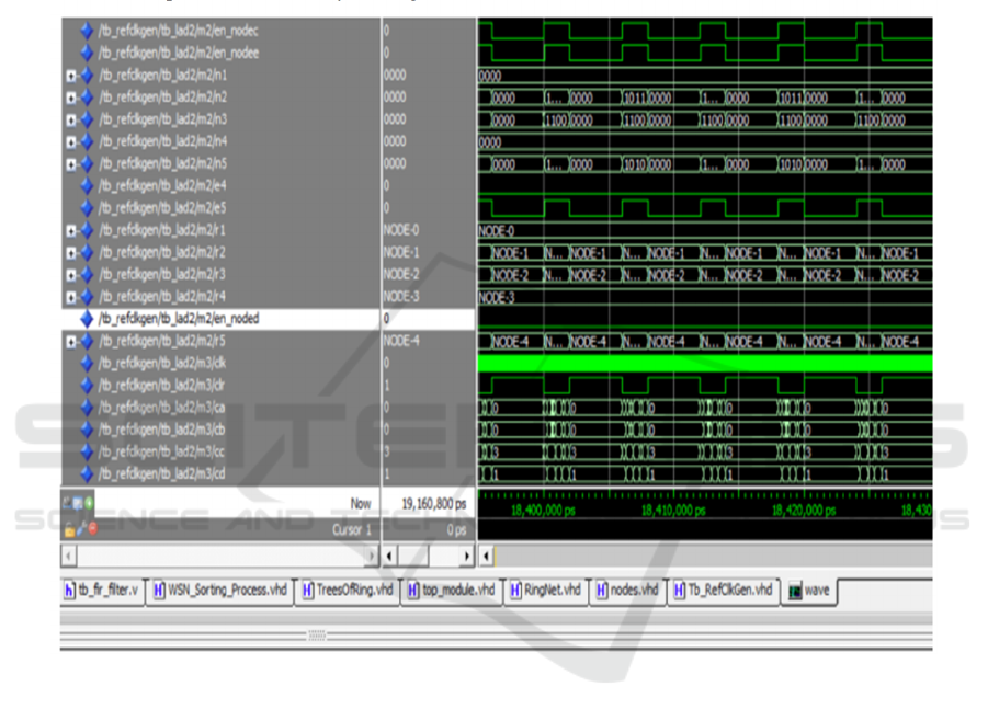
Figure 4: Node Switching.
Figure 4 illustrates the node switching activity
within the network. Depending on the control logic
and the state of routing, several nodes designated
NODE-0 through NODE-4 are in dynamic state
changes. From the waveform, nodes demonstrate that
they can be cyclically switched from active to idle
with the main clock. In the NoC, the switching of each
node is necessary to allow interconnect data transfers.
The observed transitions are performed with no
delays between one and transitioning to the
succeeding states and hence prove the
implementation does not exhibit control or boundary
glitches within the node-switching algorithm.
Furthermore, it is guaranteed that there are no
deadlocks within the system control and open passage
within packets and unhindered routing.
Figure 5 exhibits the simulation of control signals
pertaining to the Wireless Sensor Network (WSN).
The waveform exhibits different control parameters
like criteria, node_id, valid_node, and other
accompanying signals change with respect to time
and the operation of the system. The correct assertion
and de-assertion of these control signals ensure that
the coordination among the nodes of the network is
correct. Valid_node is a control signal which gives
out the correct control signal as an output and checks
for all the nodes and confirms whether or not all the
nodes are ready to send data. The result demonstrates
that the WSN control mechanism is operating
efficiently and ensures appropriate communication
and power distribution within the network.
ICRDICCT‘25 2025 - INTERNATIONAL CONFERENCE ON RESEARCH AND DEVELOPMENT IN INFORMATION,
COMMUNICATION, AND COMPUTING TECHNOLOGIES
830
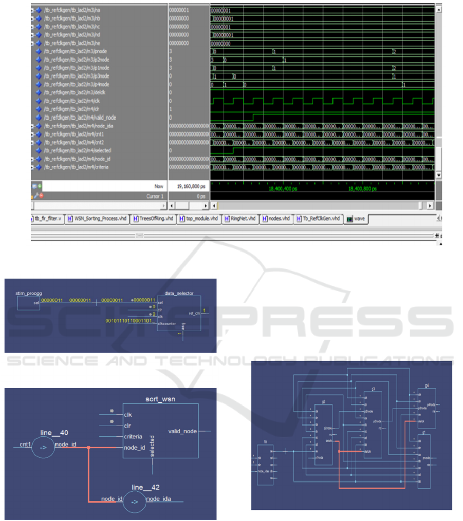
Figure 5: WSN Controls Output.
Figure 6: Internal Architecture - Data Selector and Sorting
Logic.
Figure 6 shows the internal configuration of the
data selector and sorting logic which are contained in
the design. One part of the first block depicts the
data_selector block which uses control signals sel,
clk, and clr to choose the appropriate inputs. The
second part shows the sort_wsn module which sorts
and checks nodes on a selection criterion and
generates valid_node output. Control and data paths
are distinct and separate which provide better
modularity and maintainability in the design. This
block guarantees that data is properly collected and
routed to valid nodes supplied with dynamic control
signals.
Figure 7: Internal Node Architecture.
As highlighted in Figure 7, all internal connections
among the nodes have been implemented. The
interconnections between the nodes p1, p2, p3, and p4
have been routed properly to their corresponding
control lines, data lines, and probe lines. The
connections highlighted in red designate important
data channels responsible for forwarding packets and
commanding control signals. This architecture
Development and Validation of a High-Performance Network-On-Chip Architecture with Wireless Sensor Network Controls
831

enables modular growth because more nodes can be
added with minimal effort. The accuracy and neatness
of the connections confirm the correctness of the
Network-on-Chip (NoC) topology design and
guarantee that data will be delivered to the correct
destination nodes without unnecessary delays.
5 CONCLUSIONS
In this work, a modular and scalable Network-on-
Chip (NoC) architecture was designed, verified, and
validated using VHDL, which was simulated through
ModelSim. The Designed Integrated System included
other fundamental blocks like the clock distribution
network, the 32-bit accumulator, the node switching
logic, and the WSN control. Verification of all
modules was completed through functional
verification, while timing and physical verification
were done to ensure all fundamental milestones were
achieved: meeting design constraints, power budget,
and compliance to design rules. The simulations
confirmed functionality with respect to clock
generation, data accumulation, node switching, and
WSN control; all of which are requirements for high-
performance and embedded designs. The entire
system showcased low latency and power
consumption with flexibility, demonstrating
applicability to larger SoC platforms and real-time
systems. In the future, the design could benefit from
implementing the chip into silicon, advanced low-
power techniques such as clock gating and multi-
voltage domains, increasing the node expansion, and
adding adaptive traffic routing algorithms.
Furthermore, adding fault tolerance and security
features would strengthen the reliability of the NoC
for mission-critical uses like IoT industrial
applications and autonomous systems. To conclude,
the created NoC framework offers extensible
prospects for additional pre-commercial and
scholarly exploration, thereby facilitating the
construction and refinement of more sophisticated
on-chip communication networks.
REFERENCES
Brown, J.K., et al., 2020. 27.1 A 65nm energy-harvesting
ULP SoC with 256kB Cortex-M0 enabling an 89.1µW
continuous machine health monitoring wireless self-
powered system. In: IEEE International Solid-State
Circuits Conference (ISSCC). pp.420–422.
Cheng, Y.H., Huang, L.B., Cui, Y.J., Ma, S., Wang, Y.W.
and Sui, B.C., 2022. RV16: An ultra-low-cost
embedded RISC-V processor core. Journal of
Computer Science and Technology, 37, pp.1307–1319.
Chou, T.H., Yu, S., Bose, S., Cook, J., Park, J. and
Johnston, M.L., 2023. Wireless, multi-sensor system-
on-chip for pH and amperometry powered by body
heat. IEEE Transactions on Biomedical Circuits and
Systems, 17(4), pp.782–794.
Duran, C., et al., 2016. A 32-bit RISC-V AXI4-lite bus-
based microcontroller with 10-bit SAR ADC. In: IEEE
Latin American Symposium on Circuits and Systems
(LASCAS). pp.315–318.
Hasegawa, T., et al., 2017. SOTB (Silicon On Thin Buried
Oxide): More than Moore technology for IoT and
automotive. In: IEEE International Conference on IC
Design and Technology (ICICDT). pp.1–4.
Lim, W., Lee, I., Sylvester, D. and Blaauw, D., 2015. 8.2
Batteryless sub-nW Cortex-M0+ processor with
dynamic leakage-suppression logic. In: IEEE
International Solid-State Circuits Conference (ISSCC).
pp.1–3.
Lin, L., Jain, S. and Alioto, M., 2018. A 595pW 14pJ/cycle
microcontroller with dual-mode standard cells and self-
startup for battery-indifferent distributed sensing. In:
IEEE International Solid-State Circuits Conference
(ISSCC). pp.44–46.
Lukas, C.J., et al., 2023. 15.2 A 2.19µW self-powered SoC
with integrated multimodal energy harvesting, dual-
channel up to -92dBm WRX and energy-aware
subsystem. In: IEEE International Solid-State Circuits
Conference (ISSCC). pp.238–240.
Myers, J., et al., 2015. 8.1 An 80nW retention 11.7pJ/cycle
active subthreshold ARM Cortex-M0+ subsystem in
65nm CMOS for WSN applications. In: IEEE
International Solid-State Circuits Conference (ISSCC).
pp.1–3.
Sarmiento, M., et al., 2021. A sub-µW reversed-body-bias
8-bit processor on 65-nm silicon-on-thin-box (SOTB)
for IoT applications. IEEE Transactions on Circuits and
Systems II: Express Briefs, 68(9), pp.3182–3186.
Sarmiento, M., et al., 2022. Systems on a chip with 8-bits
and 32-bits processors in 0.18-um technology for IoT
applications. IEEE Transactions on Circuits and
Systems II: Express Briefs, 69(5), pp.2438–2442.
Schiavone, P.D., et al., 2017. Slow and steady wins the
race? A comparison of ultra-low-power RISC-V cores
for Internet-of-Things applications. In: International
Symposium on Power and Timing Modeling,
Optimization and Simulation (PATMOS). pp.1–8.
Schoeberl, M., 2011. Leros: A tiny microcontroller for
FPGAs. In: International Conference on Field
Programmable Logic and Applications (FPL). pp.10–
14.
Serrano, R., et al., 2021. A low-power low-area SoC based
in RISC-V processor for IoT applications. In:
International SoC Design Conference (ISOCC).
pp.375–376.
Tran, T.A. and Ishibashi, K., 2022. High-accuracy and
long-range energy harvesting beat sensor with LoRa.
In: IEEE Sensors. pp.1–4.
ICRDICCT‘25 2025 - INTERNATIONAL CONFERENCE ON RESEARCH AND DEVELOPMENT IN INFORMATION,
COMMUNICATION, AND COMPUTING TECHNOLOGIES
832
