
Efficient Three Operand Adder Design with Carry Prefix Logic for
Reduced Delay
Divya S
1
, Mohankumar M
2
, Dhanasekar J
2
, Krishnaraj R
3
, T. Senthil
4
and Vikram N
5
1
VLSI Design, Sri Eshwar College of Engineering, Coimbatore, Tamil Nadu, India
2
Department of Electronics and Communication Engineering, Sri Eshwar College of Engineering, Coimbatore,
Tamil Nadu, India
3
Department of Electronics and Communication Engineering, Bannari Amman Institute of Technology, Sathyamangalam,
Tamil Nadu, India
4
Department of Computer Science and Engineering, Sreenivasa Institute of Technology and Management Studies, Chittoor,
Andhra Pradash. India
5
Department of Electronics and Communication Engineering, Sona College of Technology, Salem, Tamil Nadu, India
Keywords: Carry Save Adder (CSA), Three-Operand Binary Adder, Han-Carlson Adder (HCA), Low Power, and High
Speed.
Abstract: Cryptography and pseudorandom number generators are essential tools from the modern digital world. For
performance improvement adder implementations like (CS3A) and (HCA) are frequently employed. But
these adders exhibit high propagation delays that reduce the efficiency of the system. A new three-operand
binary adder architecture is presented that utilizes carry-prefix logic to achieve low power and propagation
delay. The design below obtains a log₂n time complexity via pre-computed bitwise addition, followed by a
carry-prefix compute. The proposed design was implemented with Xilinx ISE 14.7, showing that it is
power efficient and less delay-centric than CS3A and HCA adders. These results attest to the fact that the
proposed architecture can be utilized to enhance the performance of a digital system.
1 INTRODUCTION
An adder is a basic digital circuit that adds numbers,
and is a crucial building block in processors and
arithmetic logic units (ALUs). Its importance
extends to functions like address computation, table
index generation or incrementing and decrementing
in numerous digital architectures. A well-known
type of adder is the Binary Adder which can use
simple gates like AND and XOR to implement. The
type of adder we will be using adds two single-bit
binary numbers together, outputting both a carry-out
(COUT) bit as well as the sum. The Binary Adder
uses the forumal of binary additions, where sum of
any two bits will generate carry or a sum. In modular
arithmetic, frequently used in cryptographic
algorithms and pseudo-random bit generator
(PRBG) techniques, the CS3A method is one of the
most space-efficient and commonly used methods to
add three operands. The CS3A method adopts the
PP2A method, which is similar in structure to the
HCA, to new outweighing time of the critical path.
The compact design is essential for VLSI (Very
Large Scale Integrated) circuits as it enables binary
addition over three operands whilst consuming little
hardware. Such optimization is needed since they
will need to run the fastest and most space-wise
regardless of whether they are cryptographic
applications or any other digital systems.
2 LITERATURE REVIEW
CSCM: A Carry Save Adder (CSA) design reducing
power and delay. The CSA design is optimized to
address key path delays and energy efficiency
issues. The proposed method enhances performance
metrics compared to traditional CSA designs
through a systematic design review and
enhancement process. The results indicate that the
enhanced CSA is suitable for computational
processes that need less power and high speed
Divya, S., Mohankumar, M., Dhanasekar, J., Krishnaraj, R., Senthil, T. and N., V.
Efficient Three Operand Adder Design with Carry Prefix Logic for Reduced Delay.
DOI: 10.5220/0013890100004919
Paper published under CC license (CC BY-NC-ND 4.0)
In Proceedings of the 1st International Conference on Research and Development in Information, Communication, and Computing Technologies (ICRDICCT‘25 2025) - Volume 2, pages
795-799
ISBN: 978-989-758-777-1
Proceedings Copyright © 2025 by SCITEPRESS – Science and Technology Publications, Lda.
795
(Krishna Vamsi, et, al 2018) Adiabatic logic is used
for high-speed arithmetic operations that provide
acceptable performance at lower power operating;
(Nagesh N, et, al, 2018) which not only guarantees
low energy dissipation during the entire addition
process, but also helps to reduce the operation delay.
In this proposed architecture, energy consumption
and performance are optimized by using different
adder types to perform the addition of wide
operands (Jafarzadehpour, A, et, al, 2019). By
combining Transmission Gate Logic (TGL) and
CMOS we maximize the size, delay and power
consumption in hybrid architecture. This approach
avoids the drawbacks of classical RCAs through
enhanced speed and minimized power dissipation.
This indicates that the design can be used for low-
power purpose applications and offers an improved
performance over traditional methods. (Bagwari, A,
et, al, 2019). This design would optimize the carry
generation and propagation structure to speed up a
parallel prefix adder. For large operand sizes, this
architecture provides a speedup for addition overall,
as the latency of the critical path is significantly
reduced. The proposed adder is quicker than
traditional adder architectures, making it suitable for
demanding applications where high-speed
arithmetic processing is crucial (Knowles, S, et, al,
2001).
3 16 BITS THREE - OPERAND
BINARY ADDER
This section presents a new adder architecture for
adding three operands in modular arithmetic and its
corresponding VLSI implementation. The proposed
adder is a Parallel Prefix Adder (PPA) with a four-
stage structure, unlike a traditional prefix adder,
which follows a three-stage structure. There are four
stages of the adder: bit-addition logic, basic logic,
carry prefix logic, and sum logic. The first stage of
the bit-addition logic stage adds the three n-bit
binary input operands bit by bit via an array of full
adders. The full adder generates two outputs, C
(carry) and S (sum). In this step, each complete
adder will perform the addition of the bits a, b, and c
(the previous carry that is coming from 1 or 0) and
the next input bits will be executed at the basic logic
stage, so that they can prepare the operands for the
carry and propagate these findings. Stage 2:
Fundamental Logic Stage. During this stage,
generate and propagate signals are calculated. This
processing of the output signals of the full adders
(from the preceding stage). In particular, the sum
from the full adder and the carry of the full adder to
the right. We use the squared saltire-cell to illustrate
these calculations. The calculation of both generate
and propagate signals use this saltire-cell structure (n
+ 1 saltire-cells in the base logic stage). The method
aids in speeding up the carry propagation and the
sum calculation during the addition of three
operands in modular arithmetic applications and
helps provide faster VLSI design with minimum
space and time complexity.
Gi: i = Gi = Si · Cyi − 1 (1)
Pi: i = Pi = Si ⊕ Cyi − 1 (2)
For three-operand addition, the proposed adder
algorithm additionally considers the external carry-
input signal (Cin). As you can see, in the first
saltire-cell of the base logic, this additional carry-
input signal (Cin) is collected and continues to exist
within the logic, used to calculate the G0 (S Cin ));
According to the logical equation combine the black
and grey cell logics to realize the carry generate Gi:
j, and propagate Pi: j signals in the third stage,
called the “generate and propagate logic” (PG) stage
for pre-analysis of carry bit:
Gi: j = Gi: k + Pi: k · Gk − 1: j (3)
Pi: j = Pi: k · Pk − 1: j (4)
The final phase is represented as sum logic, in
which the "sumbits from the carry create Gi:j and
carry propagate Pi bits are calculated using the
logical expression 𝑆𝑖 = (𝑃𝑖⊕𝐺𝑖−1:0). The carryout
signal is directly produced by the carry generator.
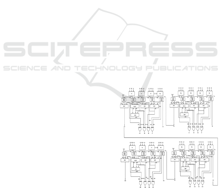
Figure 1: Block diagram of 16 bit Three operand Binary
Adder.
ICRDICCT‘25 2025 - INTERNATIONAL CONFERENCE ON RESEARCH AND DEVELOPMENT IN INFORMATION,
COMMUNICATION, AND COMPUTING TECHNOLOGIES
796
4 CARRY SAVE ADDER
A digital adder known as a carry-save adder, or
CSA, is primarily used to effectively calculate the
sum of at least three binary values. A binary
multiplier typically uses a CSA since it adds the two
binary numbers mentioned above once they have
been multiplied. This technique allows for the
implementation of a large adder, which is
significantly faster than adding numbers as is
customary. The process of adding together binary
bits involves preserving the carry and sum bits in the
first step before moving on to the second.
The stored carry and sum bits are added in this
step, which functions similarly to a ripple carry
adder, or RCA. This adder uses three operands, such
as a, b, and c, where "c" is a four-bit input carry. In
this case, all four FAs, a, b, and c are utilized. The
sum and carry bits are generated for each FA. In this
case, the carry bits are simply kept and added up to
the next sum term using a ripple carry adder rather
than being sent to the following FA.
The primary function of a carry save adder is to
calculate the sum of at least three n-bit binary
values.
A full adder and this kind of adder are
comparable. Each adder in the carry save unit
computes a single sum and carry bit based only on
the equivalent two input number bits. Assume that,
in the example below, two 4-bit values, such as a &
b, produce the partial sum "S" and carry "C."
𝑆 = 𝑎 𝑥𝑜𝑟 𝑏 𝐶 = 𝑎 𝑎𝑛𝑑 𝑏 (5)
The carry sequence "C" can be moved one position
to the left. Put a zero on the partial sum sequence
"S"'s front MSB. Ultimately, these two are added
and the final sum is produced using a ripple carry
adder, or RCA. This adder's primary job is to create
two numbers, sum "S," and carry C by adding three
k-bit integers, such as a, b, and c. While the carry
generator is used to generate the output carry
regardless of the input carry, the carry propagator is
used to propagate to the next level.
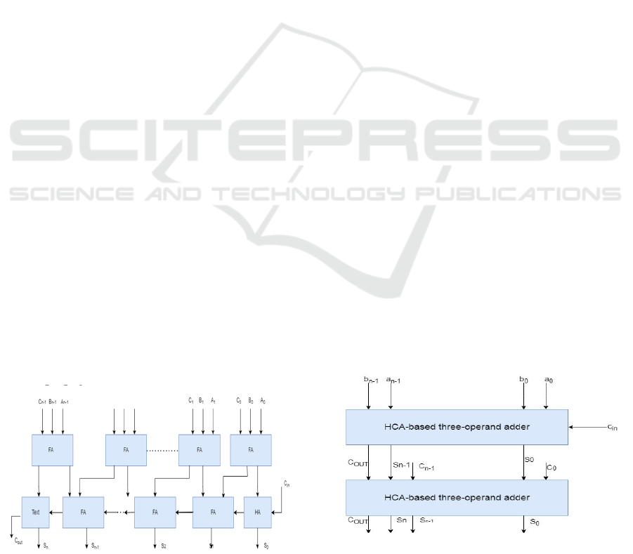
Figure 2: Block diagram of Carry save adder.
Two of the carry's functions are generation and
propagation. While the carry generator (Cg) is
employed, the carry propagation (Cp) is spread to
the next level to produce the output carry regardless
of the input carry. When calculating the sum of
several numbers, the Carry Save Adder is frequently
utilized. It conducts the final addition after storing
and transporting the partial results independently.
Although it's effective for some multi-operand
addition workloads, simple two-input addition
procedures don't usually employ it.
5 HAN-CARLSON ADDERS
Han and Carlson (1987) introduced the Han-Carlson
adder to strike a balance between the number of
computational nodes, interconnects, and logic depth
in digital adders. A network formed by combining
the Kogge-Stone and Brent-Kung adders is known
as a Han-Carlson tree. This adder applies the Brent-
Kung method for the outer rows of the prefix tree,
while using the Kogge-Stone approach for the inner
rows. When compared to the Kogge-Stone adder,
Han-Carlson prefix trees require fewer logic cells
and fewer interconnects, but at the cost of an
additional logic level for carry merging to determine
missing carries. The number of logic levels is given
by the formula [log2 (n) + 1], where "n" represents
the number of bits in the operands. Brent-Kung is
applied at the beginning and end of the prefix graph,
while the first and middle stages of the adder involve
black and grey cells positioned at odd bit positions.
In the final stage, where carry merging occurs, only
grey cells are used at the even bit positions. Overall,
the Han-Carlson adder provides a good compromise
between fan-out, the number of logic cells, and the
black cell count, making it an efficient choice
compared to the Kogge-Stone adder. The adder must
be quick and, secondly, efficient in terms of chip
area and power consumption.
Figure 3: Block level diagram of HCA-based Three-
Operand Adder (Hc3a).
Efficient Three Operand Adder Design with Carry Prefix Logic for Reduced Delay
797
A solid theoretical foundation for creating a variety
of designs is provided by parallel prefix adders.
trade-offs between power, area, and delay. The
design is modularized by dividing it into trees of
smaller and quicker adders that are easier to
implement because the adders with the massive
complex gates will be too sluggish for VLSI. Tree
adders, or parallel prefix adders, are commonly used
in digital circuits due to their ability to reduce delay,
especially in large adders where the carry
propagation dominates. High-speed addition relies
on the prior carry to produce the correct sum. Any
reduction in latency in integer addition leads to
higher throughput. As technology scales to the
nanoscale range, it becomes increasingly important
to design addition algorithms that not only deliver
excellent performance but also consume less power.
Parallel prefix adders are particularly well-suited for
VLSI (Very Large-Scale Integration)
implementation because they use simple cells and
maintain regular connections between them, making
them efficient for high-density integration. These
adders can be described in terms of wiring tracks,
fan-out, and logic levels, all of which influence their
performance. Prefix cells are typically constructed
using complex gates, along with zero or more
inverters to buffer their outputs. CMOS technology
is commonly used to build these gates. In this design
approach, buffers are employed to manage fan-out
and reduce gate loading, as excessive fan-out can
negatively affect performance.
6 RESULT AND DISCUSSION
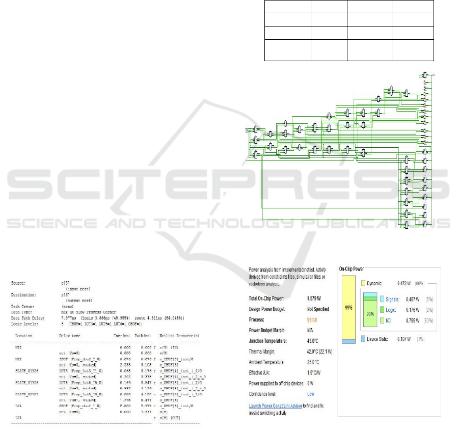
Figure 4: Delay Report of 16 bits Three operand Binary
Adder.
The TOBA achieves lower power and latency using
a four-stage parallel prefix adder, which minimizes
the fan-in and fan-out. Using an external carry-input
(Cin) is a way to optimize performance by
calculating, generating and propagating signals. The
adder is more efficient in execution, even with a
critical path delay of O (log2n + 1). It results in
faster computation and lower power consumption
than CS3A and HCA adders. This architecture
impacts scalability and speed and is suitable for
pseudorandom number generation and cryptographic
applications.
Table 1: Power, Delay, and Area Analyzis Report.
DESIGN AREA POWER DELAY
CSA 16 14.914W 7.38ns
HCA 24 11.046W 10.15ns
BINARY
ADDER
17 9.579W 7.97ns
Figure 5: RTL Schematic of 16 bit Three operand Binary
Adder.
Figure 6: Power Report of 16 bit Three operand Binary
Added.
ICRDICCT‘25 2025 - INTERNATIONAL CONFERENCE ON RESEARCH AND DEVELOPMENT IN INFORMATION,
COMMUNICATION, AND COMPUTING TECHNOLOGIES
798
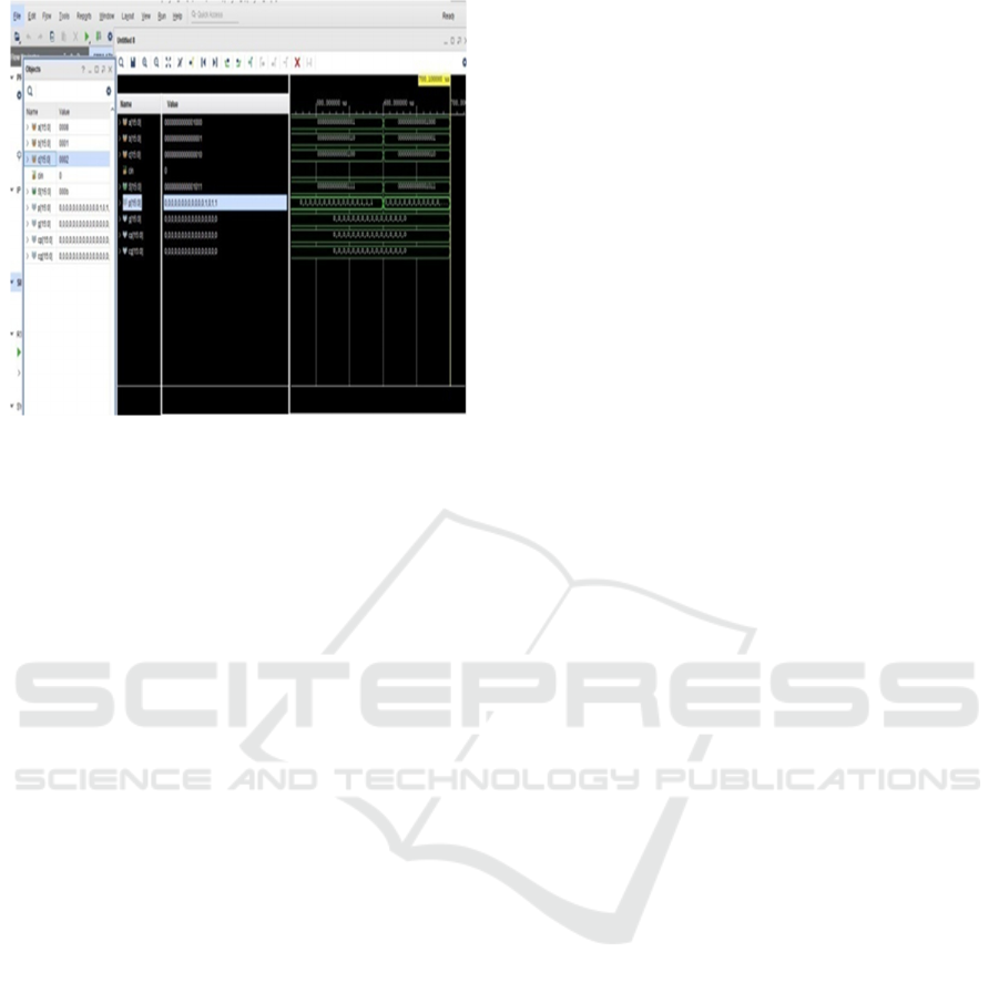
Figure 7: Simulation of 16 bit Three operand Binary
Adder.
7 CONCLUSIONS
Next, the high speed, low power three input (binary)
adder proposed here represents a considerable
progression in the design of digital systems,
especially for use in applications of significance like
RSA Cryptography and Pseudorandom Bit
Generators. The critical path delays of O(log2n) are
achieved by using pre-computed bitwise addition
and carry-prefix computation, outperforming
traditional designs like CS3A and HCA. The
implementation utilizing Vivado 2023.1
corroborated its superiority one more time also it
showed less power dissipation, area usage, Power-
Delay Product (PDP), Area-Delay Product (ADP)
When compared with the CS3A having area of 16,
power of 14.914 W and delay of 7.38 ns and HCA
with area of 24, power of 11.046 W and delay of
10.15 ns, the area, power and delay of proposed
adder were found to be 26, 9.579 W and 7.97 ns
respectively. These features make it well-equipped
for environments that are resource-scarce and need
high-speed, energy-efficient solutions.
REFERENCES
Krishna Vamsi, A., Udaya Kumar, N., BalaSindhuri, K.,
Sai Chandra Teja, G., “A Systematic Delay and Power
Dominant Carry Save Adder Design,” 2018
International Conference on Smart Systems and
Inventive Technology (ICSSIT), 2018.
Nagesh N. Nazare, R. J. Nayana, Pradeep S. Bhat, and
B.S. Premananda, "Design and Analysis of Low-
Power 16-bit Parallel-Prefix Adiabatic Adders," 2018
3rd IEEE International Conference on Recent Trends
in Electronics, Information & Communication
Technology (RTEICT), 2018.
Jafarzadehpour, A. S., Molahosseini, A. S.,
EmraniZarandi, A. A., and Sousa, L., “New Energy-
Efficient Hybrid Wide-Operand Adder Architecture,”
IET Circuits, Devices & Systems, November 2019.
Bagwari, A., and Katna, I., “Low Power Ripple Carry
Adder Using Hybrid 1-Bit Full Adder Circuit,” 2019
11th International Conference on Computational
Intelligence and Communication Networks (CICN),
2019.
Knowles, S., “A Family of Adders,” Proceedings of the
15th IEEE Symposium on Computer Arithmetic
(ARITH), June 2001.
MuthyalaSudhakar, S., Chidambaram, K. P., and
Swartzlander, E. E., “Hybrid Han-Carlson Adder,”
Proceedings of the IEEE 55th International Midwest
Symposium on Circuits and Systems (MWSCAS),
Boise, ID, USA, August 2012.
Bagwari, A., and Katna, I., “Low Power Ripple Carry
Adder Using Hybrid 1-Bit Full Adder Circuit,” 2019
11th International Conference on Computational
Intelligence and Communication Networks (CICN),
2019.
R.P. Brent and H.T. Kung, “A Regular Layout for Parallel
Adders,” IEEE Transactions on Computers, Vol. C-
31, pp. 260-264, 1982.
Ibrahim, A., Gebali, F.: ‘Optimized structures of hybrid
ripple carry and hierarchical carry lookahead adders’,
Microelectron. J., 2015, 46, (9), pp.783–794.
Mohanty, B.K., Patel, S.K.: Area-delay-power efficient
carry select adder IEEE Trans. Circuits Syst.-II:
Express Briefs, 2014, 61, (6), pp. 418–422’.
K. R, S. T, V. N, S. B and S. A, "Design of a Sleep
Transistor and Read, Write Separation based 6T
SRAM Memory Array for Low Power IOT
Applications," 2021 Smart Technologies,
Communication and Robotics (STCR),
Sathyamangalam, India, 2021, pp. 1-5, doi:
10.1109/STCR51658.2021.9588951.
Efficient Three Operand Adder Design with Carry Prefix Logic for Reduced Delay
799
