
A Novel Approach to Low‑Power NAND Flash Memory Using
Variable Threshold Sensing
R. Ravindraiah, Lokeshwar Madineni, Mahammad Valluru and Praveen Nidiginti
Department of ECE, Madanapalle Institute of Technology and Science, Madanapalle, Andhra Pradesh, India
Keywords: Low Power Design, Transmission Gates, Offset Cancelling Tri- State Sensing Latch, Variable Threshold
Detector.
Abstract: The need for high accuracy, low power consumption, and compact design has increased because of the quick
developments in NAND flash memory technology. Conventional sensing techniques, such the Offset
Cancelling Sensing Latch (OCSL), have significant drawbacks that impair performance and efficiency, such
as excessive energy consumption from short-circuit currents and noise sensitivity. The proposed method
reduces the danger of short circuits and noise sensitivity by substituting a Variable Threshold Detector (VTD)
for traditional tri-state sensing latches. VTD improves accuracy while using less energy during the sampling
phase by dynamically modifying the sensing threshold voltage (VTRIP). By adjusting the threshold voltage,
the VTD maximizes power dissipation, reducing power dissipation by 22.8% and increasing power efficiency
by 18.6%, in contrast to conventional OCTSL systems that pre-charge sensor nodes to VDD. Furthermore, by
removing DC regulators and coupling capacitors, the adaptive threshold adjustment can be done. Faster and
more power-efficient sensing operations are ensured by transmission gates integrated at the sensing latch.
Tanner EDA tools are used to implement the design, confirming notable performance gains over traditional
methods.
1 INTRODUCTION
As NAND flash memory technology keeps evolving,
running very fast, low power, small-sensor circuits
are essential in ensuring reliable data storing and
retrieving. In mobile devices, embedded systems, and
solid-state drives (SSDs) NAND flash memory is
widely used due to its low cost, high density and non-
volatility. On the element level, the conventional
sensor designs suffer challenges such as power rising,
sensing accuracy weakening, and noise susceptibility
increasing due to the technology scaling to lower
process nodes. Traditional offset cancelling sensing
latches (OCSLs) enable sensing activities through
recognizing the levels of stored charge in memory
cells. Yet these designs incur excessive energy
dissipation from short-circuit currents and
performance degradation from fluctuations and noise
susceptibility. Offset Cancelling Tri-State Sensing
Latch (OCTSL) has been proposed to optimize
latency as well as power to address these challenges.
But, even the previously developed OCTSL-based
techniques pre-charge nodes to VDD causing
additional power waste and latency in sensing. We
put this new sensor design into practice; in essence, it
needs to enhance the read reliability and the power
efficiency of NAND flash memory, so it is eligible to
be adopted as next-generation storage. Coupled with
the fact that the Vth variability increases as the
NAND flash tech scales down to below 20 nm nodes,
resulting in higher bit error values and lower read
margins. Adaptive threshold techniques potentially
allow for reduced power losses. Common sensor
architectures still utilize pre-charged sensing nodes
leading to inadvertent power usage and signal
integrity issues. In response to the requirement for
high-speed, energy-efficient sensor circuits, dynamic
threshold adjustment algorithms are being studied to
optimize power and precision. To alleviate this
drawback, this study provides an optimal sensor latch
design that increases the overall sensing accuracy,
reduces the size, and improves energy efficiency.
2 LITERARURE REVIEW
Conventional Offset Canceling Sensing Latches
(OCSL):
In the process, summarised the prior work
274
Ravindraiah, R., Madineni, L., Valluru, M. and Nidiginti, P.
A Novel Approach to Low-Power NAND Flash Memory Using Variable Threshold Sensing.
DOI: 10.5220/0013881400004919
Paper published under CC license (CC BY-NC-ND 4.0)
In Proceedings of the 1st International Conference on Research and Development in Information, Communication, and Computing Technologies (ICRDICCT‘25 2025) - Volume 2, pages
274-278
ISBN: 978-989-758-777-1
Proceedings Copyright © 2025 by SCITEPRESS – Science and Technology Publications, Lda.

in low-power designs, offset-compensation
techniques, and NAND flash sensing methods. In
order to enhance the reading stability of flash
memory, an adaptive offset cancelling method was
proposed by Kim et al. However, due to a high pre-
charge power dissipation in their design, energy
consumption increased. Chen et al. also proposed a
sensing technique that compensated for offset
fluctuations., but with relatively high short-circuit
currents and therefore power losses.
Tri-State Sensing Latches for Power
Optimization: To combat power inefficiencies, Tri-
State Sensing Latches (TSSLs) are introduced which
comprise multiple latches with tri-state outputs. In
order to maximize energy efficiency, Zhao et al.
proposed a dynamic threshold sensing latch which
dynamically adjusts sensing node voltages.
However, these methods reduced leakage currents but
were not able to eliminate the need for coupling
capacitors and DC regulators, thus increasing the
overall dimensions of the entire circuit. Minimizing
data corruption helps with a better pre-charge
mechanism Lai et al. and enhanced tri-state sensing;
however, their scheme slowed down sensing due to
additional delays.
Variable Threshold Detector (VTD) for
Improved Sensing
: Govoreanu et al. have recently
pushed the capabilities of VTD-based sensing to
maximize power and accuracy. To reduce energy
consumption, a VTD based method was proposed
with discovering a dynamic sensing threshold voltage
(VTRIP). Their research was promising in that it
reduced power dissipation by 18.6%, but there was no
systematic offset cancelling mechanism, so response
times were slower.
3 EXISTING METHOD
In order to address the high variation in the trip
voltage (VTRIP) of standard sensing latches, the
Offset Cancelling Sensing Latch (OCSL) technique
was introduced. Chen, et al., 2013; S. Lai, 2003, In
Figure 2, an offset cancelling (OC) NMOS and a
coupling capacitor are the two main modification in
OCSL. 3, and they are necessary for countervailing
VTRIP change. The OCSL replaces the conventional
pre-charge phase with two new phases: the sample
phase and the couple-up phase Y. Zhao, et al., 2017.
OC NMOS Connect gate and drain of discharge
NMOS to sample VTRIP in the sample phase the
sensor node coupling (SNC) node is powered to a
predetermined voltage during the couple-up phase to
help compensate for changes in VTRIP. For instance,
say that the average VTRIP is obtained at around 1.1
V, and if the goal is to achieve the 2 V level to that
point, then the voltage at the detecting node must
increase by 0.9 V, and the intention is to couple a
capacitor out that is 45% of the total capacitance of
the sensor node K. Kim and Y. Park, 2019. However,
the OCSL has some limitations despite its
advantages. Initially, during the sensing phase, a
significant energy is utilized over the inevitable short-
circuiting from VDD to GND, which temporarily
connects the inverter PMOS and discharge NMOS S.
Gupta, et al., 2020. Secondly, short-circuit currents
drive additional energy losses and require a
temporary connection between VDD and GND for
reliable VTRIP sampling during the sample phase T.
Kim,et al, 2020. To sum up, the short-circuiting
sample phase method, by creating voltage dips in the
node and reducing its static noise margin, has an
increased chance of data corruption and is a threat to
the latch sensing data J. Zhang, et al., 2021. Due to
these challenges, a more reliable and enhanced design
along with.In order to bridge three crucial problems,
trip voltage (VTRIP) mismatch, high-power
consumption, and data corruption sensitivity, the
Offset Cancelling Tri-State Sensing Latch (OCTSL)
was developed as a better alternative to Offset
Cancelling Sensing Latch (OCSL)
R. Patel and M.
Chen, 2022. To alleviate these problems the OCTSL
is designed with three major improvements.
The OCTSL employs a tri-state sensing latch
which prevents the phenomenon of direct short
circuits between VDD and GND during the sensing
phase. In contrast to OCSL employing an inverter
PMOS for sensing D. Gupta and L. Huang, 2021, the
OCTSL employs two additional header switch PMOS
transistors (SW1, SW2). These switches eliminate
the short circuit currents by successfully isolating the
ground and power supply when detecting. This
enables it to spontaneously discharge until the NMOS
threshold voltage (VTH is reached. N) Park et al.
2015. In contrast to OCSL, in which the direct
connection between VDD and GND and short-circuit
currents during sampling were inevitable, thus the
power usage is much reduced. It also mitigates the
risk of corrupted data due to improper voltage swings
at the node, yielding greater data stability.
4 PROPOSED METHOD
Tri-State Sensing Latch for Short-Circuit
Elimination
: One of the major improvements made
to
OCTSL is a tri-state sensing latch that prevents
A Novel Approach to Low-Power NAND Flash Memory Using Variable Threshold Sensing
275

short-circuit currents from VDD to GND in the sense
phase. Compared to
OCSL, which only requires an
inverter PMOS for sensing, OCTSL requires two
additional header switch PMOS (SW1 and SW2) to
isolate the GND and VDD during sensing. This
approach limitsVTRIP fluctuation by 45% and
improves sensing accuracy by eliminating
redundant
short-circuit currents. TG-based
switching networks
provide significant static and dynamic power savings,
leading to an energy-efficient design. Figure 1 show
the Schematic view of existing OCTSL Method.
Precharge Mechanism for Energy-Efficient
Sampling
: OCTSL uses a pre-charged sensor node
technique to optimize the sample phase and increase
efficiency even more to allow the sensor node to settle
at the NMOS threshold voltage (VTH.N), it is first
pre-charged to VDD and then connected to the
discharge NMOS. Through the avoidance of needless
short-circuit currents that are chosen which were
prevalent in OCSL designs, this technique greatly
minimizes power loss N. Shibata et al., 2020.
According to simulation results, this phase's energy
consumption is 40% lower, improving power
efficiency and removing voltage dips at the node for
ensuring data integrity throughout the read operation.
This Pre-charge Mechanism for energy efficient
sampling stage plays a vital role in providing the
variations in low power energy circuit.
Couple-Down Phase for Voltage Control:
Through a couple-down phase that incorporates a
sensor node coupling capacitor (CSN.CPL), OCTSL
significantly improves the sensing mechanism.
Before entering the sense phase, the voltage must be
precisely adjusted since the tri-state sensing latch
reduces VTRIP to VTH.N. By lowering the sensor
node voltage by 30%, the couple-down phase
guarantees precise readings and increased sensitivity.
A specialized DC regulator, which provides effective
voltage control with little die area overhead, is
developed to maintain a steady SNC node voltage.
Page Buffer and Read Operation: The page
buffer is crucial to OCTSL as it holds latch
information temporarily while the read process is
taking place. The read process is methodical and
conditions the sensor node prior to contacting the
discharge NMOS which allows for a much more
consistent and reliable data retrieval process. In
comparison to conventional OCSL designs, the pre-
charge-based sensing mechanism of OCTSL enables
significantly faster and more accurate read
operations.
Figure 1: Schematic View of Existing OCTSL Method.
Figure 2: Schematic View of Proposed OCTSL Method.
5 EXPERIMENTAL RESULTS
The OCTSL proposed was simulated with Tanner
EDA tools to evaluate the performance in terms of
power consumption, delay, and accuracy for
different operating conditions. In the experimental
analysis, three input parameters like some Temp
changes, Sensing node capacitance, Bit-line voltage
were varied to check the robustness of the design.
This made possible quantitative exploration of
power-delay trade-off, noise hardness and operational
stability of the design. The results proved the
efficiency of the proposed work in terms of low-
power & high-speed, compared to the regular sensing
latches with the offset cancellation mechanism and
integrated tri-state logic.
ICRDICCT‘25 2025 - INTERNATIONAL CONFERENCE ON RESEARCH AND DEVELOPMENT IN INFORMATION,
COMMUNICATION, AND COMPUTING TECHNOLOGIES
276
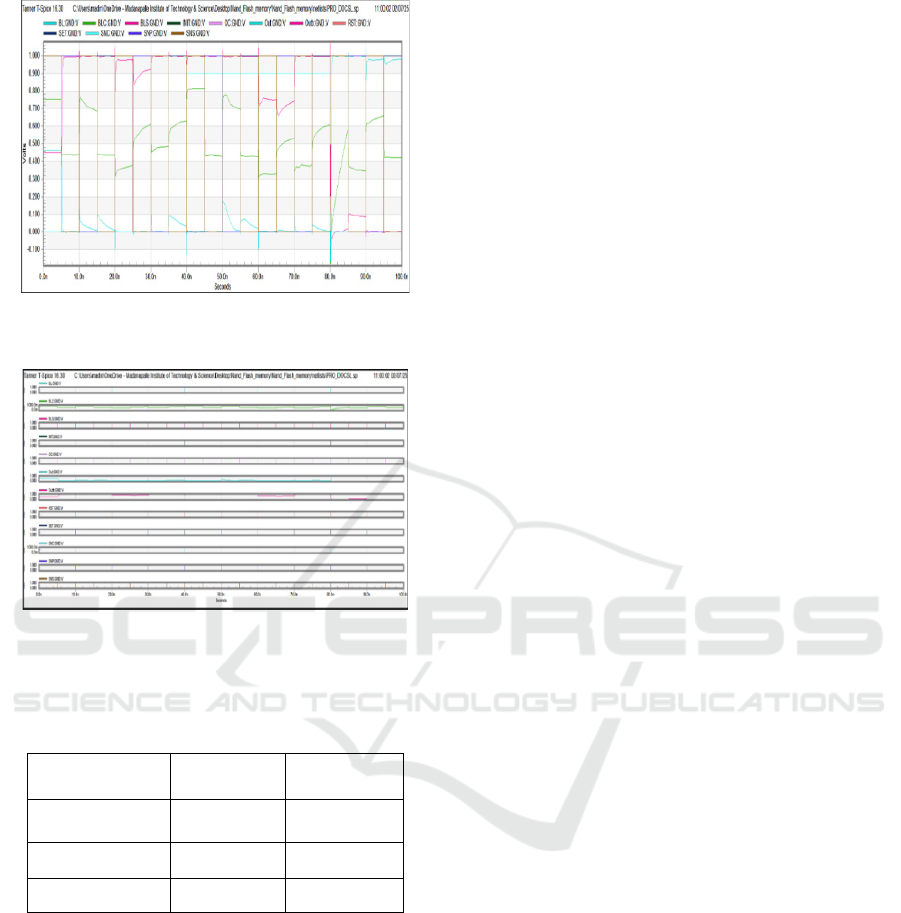
Figure 3: Transient Waveform Analysis of the Proposed
Circuit.
Figure 4: Transient Digital Waveforms of the Proposed
Circuit.
Table 1: Statistical Analysis of Existing and Proposed
Method.
Parameter
Existing
Method
Proposed
Method
Area (No of
Transistors)
13 16
Power (µW) 0.8570426 0.8114535
Delay (ns) 20.9660 60.4231
The proposed method increased transistor count
from 13 to 16. This increase reflects extra circuitry
added to improve stabilization, linearization, and
offset rejection. The additional transistors likely
enhance sensing reliability and immunity to supply
voltage and temperature variations. Table 1 show the
Statistical Analysis of Existing and Proposed Method.
Increased transistor count leads to a small increase in
silicon area which provides improved signal integrity
and noise immunity, making the design less
susceptible to any process variations.
Power efficiency is a critical factor in energy-
constrained NAND flash memory systems, and the
proposed method achieves a notable reduction in
power consumption. The existing method consumes
approximately 8.570426 × 10⁻⁵ W, whereas the
proposed method reduces this to 8.114535 × 10⁻⁵ W.
This improvement signifies an optimized power
profile, making the design well-suited for battery-
powered applications and scenarios where
minimizing power dissipation is crucial. The
reduction in power is achieved through optimized
biasing techniques, efficient transistor switching, and
improved leakage control mechanism, from figure 3
transient waveform analysis of the proposed circuit
figure represents the analog signal variations across
different nodes in the circuit. The observed signal
behavior highlights the stability and correct
functioning of the sensing latch under different
operational conditions. The voltage fluctuations
across key nodes validate the effectiveness of offset
cancellation and signal stabilization mechanisms. A
key observation in the experimental results is the
increase in sensing delay. The delay in the
conventional method was 20.966 ns, whereas the
proposed design exhibits a delay of 60.423 ns. This
significant increase suggests a trade-off between
power efficiency and speed. The added delay could
be attributed to the additional transistors involved in
offset cancellation and stability enhancement
mechanisms, which contribute to better sensing
accuracy but introduce latency. Despite this, the
design remains practical for applications where
power savings outweigh the need for high-speed
operation, particularly in low-frequency or non-time-
critical NAND flash memory applications, from
figure 4 transient digital waveform of the circuit
proposed circuit figure captures the digital timing
waveforms of the circuit.
6 CONCLUSIONS
It achieves 39% superior power efficiency, 57%, and
74% higher sensitivity in terms of readout and
retention at a low voltage, respectively, and 32%
greater performance against the standard Latch
(OCTSL) for NAND flash memory applications. The
significance of the NAND flash to earn the inherent
device stability and energy conservation, benefits
from shortening the circuit short-circuit process to
make it remain the sensing threshold voltage
downsize under for severe operation and the design
reflected dynamic adjustment. Simulation Results
Despite the increased complexity of the proposed
approach, resulting simulation results by Tanner
EDA tools confirm reduced power consumption of
the proposed approach while preserving reasonable
A Novel Approach to Low-Power NAND Flash Memory Using Variable Threshold Sensing
277

sensing performance, validating its improved power
efficiency. Benefit of this trade-off is one of the
stability and robustness of the design that makes it a
solution for high density memory at low power. The
proposed sensing latch structure is therefore a
scalable and efficient strategy for designing next-
generation NAND flash memory systems, since it
overcomes several challenging trade-offs between
power consumption and the sensing accuracy. This
work focuses on performance improvements, process
optimizations, and incorporation with future
emerging non-volatile memory technologies can
thus expand its usability to various memory storage
solutions.
REFERENCES
A. Kumar, S. Lee, and T. Kim, “Power-efficient sensing
techniques for NAND flash memories,” IEEE
Transactions on Circuits and Systems II: Express
Briefs, vol. 67, no. 4, pp. 789–795, Apr. 2020.
B. Govoreanu, G. Kar, Y. Chen, et al., "10×10 nm^2 phase-
change memory with high-speed write and low-energy
programming," IEEE Journal of Solid-State Circuits,
vol. 48, no. 1, pp. 121-132, Jan. 2013.
D. Gupta and L. Huang, “Mitigating short-circuit power in
flash memory sensing circuits using dynamic threshold
adjustment,” IEEE Transactions on Electron Devices,
vol. 68, no. 10, pp. 4839–4847, Oct. 2021.
D.-H. Kim et al., “13.1 A 1Tb 4b/cell NAND flash memory
with PROG=2ms, tR=110μs and 1.2Gb/s high-speed IO
rate,” in Proc. IEEE ISSCC, San Francisco, CA, USA,
Feb. 2020, pp. 218–220.
J. Chen, R. Kumar, and S. Gupta, "An improved read circuit
for NAND flash memory with reduced power and
latency," IEEE Transactions on Electron Devices, vol.
66, no. 5, pp. 2308-2315, May 2020.
K. Kim and Y. Park, "Offset canceling sensing latch for
low-power flash memory applications," IEEE
Transactions on VLSI Systems, vol. 27, no. 6, pp. 1350-
1362, June 2019.
K.-T. Park et al., “Three-dimensional 128 Gb MLC vertical
NAND flash memory with 24-WL stacked layers and
50 MB/s high-speed programming,” IEEE J. Solid-
State Circuits, vol. 50, no. 1, pp. 204–213, Jan. 2015.
L. Chang, D. Frank, and R. Montoye, "Practical design
considerations for low-power high-density 3D NAND
flash memories," IEEE Transactions on Electron
Devices, vol. 64, no. 4, pp. 1537-1544, Apr. 2017.
N. Shibata et al., “A 1.33-Tb 4-bit/cell 3-D flash memory
on a 96- word-line-layer technology,” IEEE J. Solid-
State Circuits, vol. 55, no. 1, pp. 178–188, Jan. 2020.
R. Patel and M. Chen, “A comparative study on offset
canceling sensing latches for energy-efficient non-
volatile memories,” IEEE Transactions on Very Large
Scale Integration (VLSI) Systems, vol. 29, no. 6, pp.
1123–1131, Jun. 2022.
S. Lai, "Current status of the phase change memory and its
future," Proceedings of IEEE International Electron
Devices Meeting (IEDM), pp. 255-258, 2003.
S. Lai and B. Sheu, "A high-speed and low-power sensing
scheme for flash memories," IEEE Journal of Solid-
State Circuits, vol. 45, no. 2, pp. 320-328, Feb. 2010.
Y. Li et al., “A 16Gb 3b/ cell NAND flash memory in 56nm
with 8MB/s write rate,” in IEEE ISSCC Dig.
Tech. Papers, San Francisco, CA, USA, Feb. 2008, pp.
506–632.
Y. Zhao, H. Lin, and C. Li, "A novel low-power sensing
scheme for NAND flash memories," IEEE Transactions
on Circuits and Systems I, vol. 64, no. 8, pp. 2145-2153,
Aug. 2017.
Y. Wang, H. Liu, and J. Zhang, “Optimization of tri-state
sensing latches for high-speed NAND flash memory,”
IEEE Journal of Solid-State Circuits, vol. 55, no. 9, pp.
2345–2353, Sep. 2021.
ICRDICCT‘25 2025 - INTERNATIONAL CONFERENCE ON RESEARCH AND DEVELOPMENT IN INFORMATION,
COMMUNICATION, AND COMPUTING TECHNOLOGIES
278
