Developments in the Study of Perovskite Light-Emitting Diode
Instability
Zili Chen
a
School of Physics and Electronic Engineering, Hengyang Normal University, Hengyang, Hunan, 421010, China
Keywords: Perovskite, Instability, Ionic Migration, Phase Separation.
Abstract: Perovskite light-emitting diodes (PeLEDs) exhibited significant potential for application in advanced
display technologies and solid state lighting (SSL), owing to their superior photoelectric performance.
However, compared with conventional LED technologies, the instability and disparities across various
aspects of PeLEDs have emerged as the primary bottleneck hindering their industrialization. This paper
systematically reviews the study of PeLEDs' instability and elucidates that the self-reinforcing feedback
cycle between ion migration and phase separation constitutes a critical mechanism underlying device
performance degradation. To enhance stability, this work discusses material innovation-based strategies
such as ion doping, ligand engineering, and dimensional regulation for component optimization.
Additionally, structural improvement approaches, including voltage reduction, insertion layers, and thermal
management, are analyzed from the perspective of device engineering. By underscoring the significance and
urgency of PeLED instability research, this paper aims to provide concrete insights and methodologies to
overcome the stability bottleneck of PeLED devices and expedite the practical implementation of
high-stability PeLEDs.
a
https://orcid.org/0009-0002-7624-2789
1 INTRODUCTION
In recent years, perovskite materials have emerged
as promising candidates for advanced display
technologies and next-generation lighting systems,
owing to the outstanding photovoltaic attributes,
including ultra-high light absorbance, balanced
charge carrier transport capabilities, adjustable
energy band structures and simple preparation
process (Fakharuddin et al., 2022; Han et al., 2022).
In terms of photovoltaic efficiency, perovskite
light-emitting diodes (PeLEDs) have achieved parity
with conventional LEDs, and in some aspects, even
surpassed them. Currently, the external quantum
efficiency (EQE) of the most advanced
monochromatic PeLEDs reached 28.7% (at 638 nm),
30.8% (at ~530 nm), and 26.4% (at 480 nm),
respectively (Kong et al., 2024; Bai et al., 2024);
However, in terms of stability, PeLEDs still have a
significant gap compared to traditional LEDs.
Commercially available LEDs need to meet a
minimum lifespan requirement of at least 10,000
hours to balance their environmental impact (Zhang
et al., 2025). Currently, the recorded lifetimes of red,
green, and blue PeLEDs are 48,000 hours (T95 at
1,000 cd/m2), 12,500 hours (T50 at 100 cd/m2), and
12 hours (T50 at 102 cd/m2), respectively (Yan et
al., 2023; Chen et al., 2023; The insufficiency and
disparity in stability, especially the obvious lag in
the development of blue PeLEDs, have become the
key bottleneck restricting the commercialization
process of PeLEDs (Bi et al., 2021).
This paper reviews the research on the instability
of PeLEDs, summarizes the instability mechanism of
the self-reinforcing feedback cycle of ion migration
and phase separation, and lists various solutions in
the dimensions of material innovation and device
engineering to overcome stability limitations, hoping
to accelerate the practical application process.
516
Chen, Z.
Developments in the Study of Perovskite Light-Emitting Diode Instability.
DOI: 10.5220/0013828600004708
Paper published under CC license (CC BY-NC-ND 4.0)
In Proceedings of the 2nd International Conference on Innovations in Applied Mathematics, Physics, and Astronomy (IAMPA 2025), pages 516-521
ISBN: 978-989-758-774-0
Proceedings Copyright © 2025 by SCITEPRESS – Science and Technology Publications, Lda.
2 INSTABILITY MECHANISM OF
PELEDS
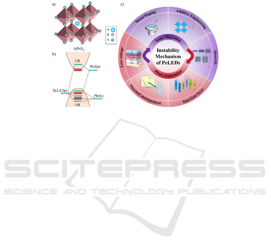
Figure 1: a) Perovskite crystal structure; b) Perovskite energy band structure; c) Instability mechanism and its optimization
strategy.
2.1 Perovskite Luminescent Materials
Perovskite materials are defined as metal halides
with an ABX3 crystal structure (Figure 1a). The
ideal perovskite crystal consists of corner-sharing
[BX6] 4-octahedra, forming an isometric system.
Here, A mainly denotes alkali metal cations or
smaller organics (Cs+, CH3NH3+, etc.), B
symbolizes mainly divalent metal cations (lead ion,
tin ion), and X represents a halide ion. Taking the
band structure of lead halide perovskites (Figure 1b)
as an example, the valence band (VB) structure
primarily arises from antibonding hybrid orbitals
formed by the interaction between X anion np
orbitals and Pb cation 6s orbitals, with the np
orbitals of halide/pseudohalide (X) components
providing the dominant contribution to the orbital
composition. The conduction band (CB) structure
originates from the hybridized interaction between
the 6p orbitals of Pb cations and the np orbitals of X
anions, with the 6p orbitals of Pb ions being
dominant. Although cations do not directly
contribute to the formation of frontier orbitals, their
differences in ionic radius can indirectly affect the
band gap width and band dispersion relationship
through lattice distortion effects (Akkerman et al.,
2018).
The unique molecular composition and band
structure of perovskites endow them with an
outstanding defect tolerance mechanism. Unlike
deep-level defects in traditional semiconductors that
significantly deteriorate carrier transport properties,
intrinsic defects in perovskites (such as vacancies
and interstitial atoms) are mostly shallow-level states
with minor impacts due to the contributions of Pb
atom's s and p orbitals (Akkerman et al., 2018).
Further, their low formation energy characteristics
cause defects to preferentially distribute in the band
edge regions near the VB top and CB bottom rather
than within the semiconductor's forbidden energy
region, thus having little effect on carrier relaxation
and recombination processes (Kovalenko et al.,
2017). This unique defect distribution pattern
effectively suppresses non-radiative recombination
channels, endowing the material with extremely high
fluorescence quantum yields (introducing TOP-PbI2
can increase the PLQY to nearly 100%), an
ultra-broad color range (close to 1.4 times the NTSC
specification), and ultra-pure color emission
characteristics (Liu et al., 2018). Combined with the
quantum confinement effect, perovskite materials
exhibit performance boundaries that surpass
traditional luminescent materials, making them
strong contenders for next-generation optoelectronic
materials and widely used in lasers, light-emitting
diodes, and next-generation displays and other
luminescent fields.
2.2 Ion Migration
The unique three-dimensional corner-sharing
[BX6]4 octahedra structure of perovskite materials,
which endows them with excellent defect tolerance,
Developments in the Study of Perovskite Light-Emitting Diode Instability
517

also constitutes a conduction path for ion migration
(mainly the migration of A and X cations).
Compared with perovskite devices, PeLEDs have
more severe ion migration phenomena. On the one
hand, the fabrication of PeLEDs usually requires the
introduction of excessive organic halide salts, where
the free halide ions (X-) and organic cations
(MA+/FA+) that do not participate in lattice
coordination form an overly concentrated ion
reservoir at the grain boundaries and surface,
providing a material basis for ion migration (Jia et
al., 2021). On the other hand, the perovskite active
layer in PeLEDs is typically only tens of nanometers
thick and needs to withstand a high voltage of >3V,
resulting in a more pronounced local Joule heating
effect (Lianfeng et al., 2017).
Such a high ion migration rate will lead to the
aggregation of vacancy defects at perovskite
interfaces, causing crystal structure distortion (Kim
et al., 2020). Lattice deformation leads to the
appearance of deep-level defect states and
non-radiative recombination centers in the device,
ultimately reducing the radiative efficiency of the
perovskite emission layer. More specifically, as
PeLED devices operate, the external electric field
will induce charged ions to cross the interface and
enter the charge transport layer (ETL), affecting the
conductivity of ETL and causing current-voltage
hysteresis. Even some Br- and CN- (MA+) ions will
form migration paths with a diameter of 25 μm, i.e.,
black spots in the device (Lee et al., 2019). Yuan et
al. (2016) pointed out that the external electric field
will also promote electrochemical reactions in
perovskite materials, accelerating the decomposition
of perovskite materials and generating gaseous
products such as AX2 and X or organic substances.
Yuan's experiments found that as the applied electric
field increased 1 V μm¹, the distance traveled by the
gas generation path over 100 μm decreased from
about 250 s to about 168 s, and the path width
further expanded. Liu et al. (2021) also noted that
the temperature rise during device operation will
lower the migration barrier, activate ion vibrations,
form defect clusters, and cause material emission
thermal quenching (enhanced electron-phonon
interaction, making it easier for exciton energy to be
dissipated through phonon scattering).
The excessive ion migration rate caused by the
preparation and luminescence of perovskite
luminescent materials leads to lattice distortion and
material decomposition, thereby reducing stability.
This is the core principle of its instability.
2.3 Phase Separation and
Environmental Impact
The microscopic kinetic origin of phase separation
phenomena is constituted by ion migration, which is
essentially a non-equilibrium transport process of
carriers at lattice defects. When the local ion
concentration exceeds the thermodynamic stability
threshold, it triggers the phase separation behavior of
the material system, forming a multi-phase
coexistence structure with different lattice constants,
bandgap energy levels, and electrical conductivity
characteristics. Wang et al. (2023) pointed out that
this non-uniform phase distribution would lead to the
interruption of carrier transport paths, specifically
manifested as a decrease in carrier mobility and a
significant quenching effect of recombination
luminescence. Baek et al. (2024) found that lattice
distortion fields are generated at the multi-phase
interfaces, inducing the initiation and propagation of
microcracks. This structural defect is significantly
enhanced by the synergy of the environment. For
instance, after heating, the film shows enlarged
grains (~50%) and cracks at the grain boundaries,
which are attributed to the displacement of A-site
cations, and this displacement is caused by the
breaking of chemical bonds under thermal effects
(Niu et al., 2017). Water and oxygen also
significantly affect PeLEDs. In a high water and
oxygen environment, water molecules are easily
adsorbed at the perovskite grain boundaries and
undergo hydrolysis reactions with organic cations
(such as MA+), leading to the decomposition of the
perovskite structure. Meanwhile, oxygen undergoes
oxidation reactions with halogen ions, generating
halogen vapor (such as I2), further exacerbating the
destruction of the lattice structure and the
deterioration of the device morphology (Yuan et al.,
2016). Xiao et al. (2017) found that after light
exposure, the Fermi level in the perovskite gap
increased by 0.3 eV, and the PL peak also showed a
slight shift, reflecting that phase separation can also
be induced by light or applied bias, and further
affecting the stability of various properties.
The above multi-scale analysis indicates that the
core instability mechanism of PeLEDs is the
self-reinforcing feedback cycle of ion migration and
phase separation. Therefore, balancing the activity
and stability of ion migration and suppressing phase
separation caused by the device electric field and the
external environment are the two key research
directions to improve the instability of PeLEDs
(Figure 1c).
IAMPA 2025 - The International Conference on Innovations in Applied Mathematics, Physics, and Astronomy
518
3 STRATEGIES FOR
IMPROVING PELEDS’
INSTABILITY
Table 1: Six Common Strategies to Improve the Instability of PeLEDs
T
50
[h] EQE[%] Strategy Ref.
5 at 3 mA/cm
2
5.10% Metal Doping
Gangishetty et al.,
2019
60 at 10 mA/cm
2
15.84% Metal Doping Li et al., 2020
12 at 102 cd/
m
2
4.70% Additive Engineering Bi et al., 2021
1340 at 100 cd/m
2
25.60% Additive Engineering Xu et al., 2025
100 at 25 mA/cm
2
5.20% Quasi-2D Shan
g
et al., 2019
7691.1 at 100 cd/m
2
27.80% Low volta
g
e Zhen
g
et al., 2024
*648,500 at 1,000 cd/m
2
23.00% Low volta
g
e Yan et al., 2023
1774 at 20 mA/cm
2
22.70% Insertion laye
r
Yi et al., 2024
4806.7 at 100 cd/m
2
21.20% Thermal managemen
t
Ye et al., 2021
*By extrapolation through an exponential model
3.1 Material Composition Engineering
By investigating the most advanced methods for
improving the stability of PeLEDs, it lists their
corresponding half-lives (T50) and external quantum
efficiencies (EQE), and summarize six common
stability improvement strategies (Table 1). Material
composition engineering is one of the core strategies
for enhancing the stability of PeLEDs, focusing on
defect passivation and lattice stiffening through
chemical composition optimization and crystal
structure regulation, thereby effectively suppressing
ion migration and slowing down the phase
separation process.
In the field of ion doping, researchers have
increased the migration activation energy of halide
ions by introducing heteroatoms, obtaining stable
perovskite crystal structures. Gangishetty et al.
(2019) partially replaced Pb2+ at the B site with
Mn2+ to obtain the multi-doped structure. The
devices showed a 5-hour brightness half-life (T50)
and excellent spectral stability, verifying the effect
of ion doping. Further, Li et al. (2020) revealed the
synergistic stabilization mechanism of alkali metal:
Cs+ uniformly distributed in the bulk enhanced
Coulomb interaction between cations and the
inorganic framework, while Rb+ preferentially
enriched at the grain boundaries and surface to
passivate defects. This dual-ion regulation extended
the device's half-life to 60 hours, highlighting the
significant contribution of multi-ion cooperative
engineering to structural stability.
In the field of ligand engineering, Bi et al. (2021)
developed a hydrogen bromide (HBr) etching
process, which was proven to remove most surface
defects and excessive carboxylate ligands from the
[PbBr6]4− octahedra. The pure blue PeLEDs
fabricated by this process had a T50 of over 12 hours
under continuous operation, setting a new record for
blue device stability. Xu et al. (2025) employed a
multisite cross-linking ligand approach to suppress
halide ion migration in CsPbBr3 QD films, which
could also effectively passivate and stabilize the
perovskite surface. This strategy increased the
device T50 to 1340 hours, more than six times
longer than traditional structures.
In the field of dimensionality control, 3D
perovskite structures were strategically modified by
substituting A cations with larger counterparts to
have quasi-2D geometries. Processed devices have
mixed phases that can achieve strong quantum
confinement. Shang et al. (2019) used a bidentate
organic molecule, BAB, as a bridging molecule to
fabricate PeLEDs, building upon the DJ framework,
with a T50 operational lifespan of 100 hours, which
is two orders of magnitude longer than that of the 3D
structure. Such quasi-2D structures balance the
requirements of carrier transport and structural
stability through the coexistence of mixed phases,
providing a new paradigm for the component design
of high-performance PeLEDs.
3.2 Device Structure Design
Device structure design is another key direction for
enhancing the stability of PeLEDs. It focuses on
optimizing the interfaces and energy level matching
between device layers to block ion migration paths
and suppress the phase separation caused by the
Developments in the Study of Perovskite Light-Emitting Diode Instability
519
coupling effect of the electric field and the
environment. It achieves a breakthrough in
long-term device stability by constructing
multi-dimensional barriers.
In terms of reducing voltage, Zheng et al. (2024)
successfully achieved a record-low 1.7 V turn-on
voltage in green PeLEDs via upgrading the emitter
and charge transfer layers, significantly increasing
the lifespan (T50 at 100 cd/m2) to 7,691.1 hours.
This study demonstrated that lowering the turn-on
voltage beneath the bandgap minimizes Joule
heating, solves stability issues, extends the
fluorescent lifetime. Yan et al. (2023) also achieved
minimal heating effect in PeLEDs through lowering
the driving voltage, achieving a high EQE of 23% at
1,000 cd/m2 and a T95 operational lifespan of over
48,000 hours.
Regarding the insertion layer, Yi et al. (2024)
proposed a spatial barrier strategy for the hole
transport layer (HTLs). Via lowering perovskite
wettability, it effectively prevents the upper HTL
from penetrating into the perovskite grain
boundaries, thereby suppressing ion migration.
Experimental data show that the device maintains a
T50 of 256 hours at a high current density of 100
mA/cm² and extends the half-life to 1,774 hours at a
low current density of 20 mA/cm². This structural
innovation provides a new approach for improving
the stability of high-brightness devices through the
synergistic effect of physical isolation and chemical
passivation.
In terms of thermal management, Ye et al. (2021)
developed a collaborative device architecture that
combines a Specially designed CsPbIxBr3-x
perovskite bulk to minimize heating effect and
enhance heat transfer of the device. This architecture
achieved a working half-life of 4,806.7 hours at 100
cd/m2. Such an architecture opens up a new path for
thermal stability management in high-performance
PeLEDs through material-structure collaborative
design.
4 CONCLUSION
This article reviews the research progress on the
stability of PeLEDs, emphasizing the critical
constraint that stability issues pose to their
commercialization process. It delves into the core
mechanism of PeLEDs' stability, highlighting the
dominant role of the self-reinforcing feedback cycle
between ion migration and phase separation in the
degradation of device performance. To enhance
stability, the article explores two major strategies:
material composition engineering and device
structure design. Although the lifespan of some
laboratory devices has reached the minimum
commercial standard for LEDs, the stability of
full-color red, green, and blue displays remains
uneven, with blue devices lagging significantly in
efficiency and lifespan. Moreover, the lack of a
unified standard for device stability testing
(inconsistent initial conditions, units, and bases, and
unknown testing environments) leads to poor data
comparability, hindering technological iteration.
Looking ahead, the stability research of PeLEDs
needs to deepen the collaborative innovation of
material gene design and device integration. On one
hand, by integrating high-throughput computing and
machine learning technologies, the screening and
optimization process of stable perovskite materials
can be accelerated. On the other hand, real-time
monitoring of ion migration/phase separation via
in-situ techniques is essential for understanding and
controlling failure mechanisms. Ultimately, through
the cross-disciplinary integration of multiple fields,
PeLEDs can be advanced towards high stability and
long lifespan for photonic applications, unlocking
their transformative potential in Environmentally
friendly lighting and flexible displays.
REFERENCES
Akkerman, Q. A., Rainò, G., Kovalenko, M. V., Manna, L.,
2018. Genesis, challenges and opportunities for
colloidal lead halide perovskite nanocrystals. Nature
Materials, 17(5).
Baek, S., Yang, S. J., Yang, H., Shao, W., Yang, Y., Dou,
L., 2024. Exciton Dynamics in Layered Halide
Perovskite Light-Emitting Diodes. Advanced
Materials, 2411998.
Bai, W., Xuan, T., Zhao, H., Dong, H., Cheng, X., Wang,
L., Xie, R.-J., 2024. Perovskite Light-Emitting Diodes
with an External Quantum Efficiency Exceeding 30%.
Advanced Materials, 35, 2302283.
Bi, C., Yao, Z., Sun, X., Wei, X., Wang, J., Tian, J., 2021.
Perovskite quantum dots with ultralow trap density by
acid etching-driven ligand exchange for high
luminance and stable pure-blue light-emitting diodes.
Advanced Materials, 33, 2006722.
Chen, W., Huang, Z., Yao, H., Liu, Y., Zhang, Y., Li, Z.,
2023. Highly bright and stable single-crystal
perovskite light-emitting diodes. Nature Photonics, 17,
401-407.
Fakharuddin, A., Gangishetty, M.K., Abdi-Jalebi, M.,
2022. Perovskite light-emitting diodes. Nature
Electronics, 5, 203-216.
Gangishetty, M. K., Sanders, S. N., Congreve, D. N., 2019.
Mn2+ doping enhances the brightness, efficiency, and
IAMPA 2025 - The International Conference on Innovations in Applied Mathematics, Physics, and Astronomy
520
stability of bulk perovskite light-emitting diodes. ACS
Photonics, 6(5).
Han, T.H., Jang, K.Y., Dong, Y., 2022. A roadmap for the
commercialization of perovskite light emitters. Nature
Reviews Materials, 7, 757-777.
Jia, Y., Yu, H., Zhou, Y., Li, N., Zhao, N., 2021. Excess
ion-induced efficiency roll-off in high-efficiency
perovskite light-emitting diodes. ACS Applied
Materials & Interfaces, 13(24), 28546-28554.
Kim, H., Kim, J. S., Heo, J. M., Pei, M., Park, I. H., Liu,
Z., 2020. Proton-transfer-induced 3d/2d hybrid
perovskites suppress ion migration and reduce
luminance overshoot. Nature Communications, 11,
3378.
Kong, L., Sun, Y., Zhao, B., Ji, K., Feng, J., Dong, J.,
2024. Fabrication of red-emitting perovskite LEDs by
stabilizing their octahedral structure. Nature,
631(8019), 73-79.
Kovalenko, M. V., Protesescu, L., Bodnarchuk, M. I.,
2017. Properties and potential optoelectronic
applications of lead halide perovskite nanocrystals.
Science, 358(6364), 745.
Lee, H., Ko, D., Lee, C., 2019. Direct evidence of
ion-migration-induced degradation of ultra-bright
perovskite light-emitting diodes. ACS Applied
Materials & Interfaces, 11(12), 11667-11673.
Li, N., Song, L., Jia, Y., Dong, Y., Xie, F., Wang, L., 2020.
Stabilizing perovskite light-emitting diodes by
incorporation of binary alkali cations. Advanced
Materials, 32(17).
Lianfeng, Z., Jia, G., YunHui, L., 2017. Electrical stress
influences the efficiency of CH3NH3PbI3 perovskite
light emitting devices. Advanced Materials, 29,
1605317.
Liu, F., Zhang, Y., Ding, C., Hayase, S., Toyoda, T., Shen,
Q., 2018. Highly luminescent phase-stable CsPbI3
perovskite quantum dots achieving near 100% absolute
photoluminescence quantum yield and application to
solar cells. JSAP Annual Meetings Extended Abstracts,
2638-2638.
Liu, M., Wan, Q., Wang, H., Carulli, F., Li, L., 2021.
Suppression of temperature quenching in perovskite
nanocrystals for efficient and thermally stable
light-emitting diodes. Nature Photonics, 1-7.
Niu, G., Li, W., Li, J., Liang, X., Wang, L., 2017.
Enhancement of thermal stability for perovskite solar
cells through cesium doping. RSC Advances, 7(28),
17473-17479.
Shang, Y., Liao, Y., Wei, Q., Wang, Z., Ning, Z., 2019.
Highly stable hybrid perovskite light-emitting diodes
based on Dion-Jacobson structure. Science Advances,
5(8), eaaw8072.
Wang, K., Lin, Z. Y., Zhang, Z., Jin, L., Ma, K., Coffey, A.
H., 2023. Suppressing phase disproportionation in
quasi-2D perovskite light-emitting diodes. Nature
Communications, 14, 397.
Xiao, Z., Zhao, L., Tran, N., Lin, Y. H. L., Silver, S. H.,
Kerner, R. A., 2017. Mixed-halide perovskites with
stabilized bandgaps. Nano Letters,
acs.nanolett.7b03179.
Xu, Y., Guo, W., Yao, J., Xu, L., Wang, J., Yang, Z.,
Wang, S., Song, J., 2025. Multisite Cross-Linked
Ligand Suppressing Ion Migration for Efficient and
Stable CsPbBr3 Perovskite Quantum Dot-Based
Light-Emitting Diodes. Angewandte Chemie
International Edition, e202422823.
Yan, G., Bo, L., Liu, X., 2023. Minimizing heat generation
in quantum dot light-emitting diodes by increasing
quasi-fermi-level splitting. Nature Nanotechnology,
18(10), 1168-1174.
Ye, Y., Li, Y., Cai, X., Zhou, W., Shen, Y., Shen, K.,
Wang, J., Gao, X., Zhidkov, I. S., Tang, J., 2021.
Minimizing Optical Energy Losses for Long-Lifetime
Perovskite Light-Emitting Diodes. Advanced
Functional Materials, 31(46).
Yi, C., Wang, A., Cao, C., Kuang, Z., Tao, X., Wang, Z.,
Zhou, F., Zhang, G., Liu, Z., Huang, H., Cao, Y., Li,
R., Wang, N., Huang, W., Wang, J., 2024. Elevating
Charge Transport Layer for Stable Perovskite
Light-Emitting Diodes. Advanced Materials, 36(31).
Yuan, Y., Wang, Q., Shao, Y., Lu, H., Li, T., Gruverman,
A., 2016. Electric-field-driven reversible conversion
between methylammonium lead triiodide perovskites
and lead iodide at elevated temperatures. Advanced
Energy Materials, 6(2).
Zhang, M., Ma, X., Esguerra, J. L., Yu, H., Hjelm, O., Li,
J., 2025. Towards sustainable perovskite light-emitting
diodes. Nature Sustainability, 8(3), 315-324.
Zheng, S., Wang, Z., Jiang, N., Huang, H., Wu, X., Li, D.,
2024. Ultralow voltage-driven efficient and stable
perovskite light-emitting diodes. Science Advances,
10(36).
Developments in the Study of Perovskite Light-Emitting Diode Instability
521
