
Graphene Two-Dimensional Heterostructure and Its Application in
High-Efficiency Optoelectronic Devices
Yunxiang Yang
1,*
a
and Heming Zhang
2
b
1
School of Materials Science and Engineering, Central South University, Changsha, 410016, China
2
Queen Mary University of London Engineering School, NPU, Northwestern Polytechnical University,
Xi’an, 710000, China
*
Keywords: Graphene, Solar Cell, Two-Dimensional Heterostructure, Optoelectronic Device.
Abstract: Graphene is a highly promising material for future optoelectronic devices due to its outstanding electronic
and optical characteristics. Its integration into advanced systems offers solutions to the stability challenges
faced by traditional solar cells. This article begins by outlining the chemical vapor deposition methods used
to synthesize high-quality graphene and discusses strategies for optimizing its interface engineering within
devices. These developments are shown to improve the separation and transport of photogenerated carriers in
two-dimensional heterostructures, thereby boosting photoelectric conversion efficiency. Moreover,
graphene’s outstanding conductivity and high optical transparency. make it ideal for applications as
transparent electrodes, carrier transport layers, and enhancements to photoactive materials. By systematically
examining these roles, the article highlights graphene’s transformative potential in optoelectronics while also
addressing the technical challenges and future application prospects. Overall, graphene has the potential to
play a central role in the evolution of optoelectronic technologies, with ongoing research paving the way for
practical and scalable implementations.
1 INTRODUCTION
As a groundbreaking two-dimensional material,
graphene has drawn considerable interest in
optoelectronics due to its remarkable electronic,
optical, and mechanical properties. Its ultra-high
carrier mobility, wide spectral absorption range,
ultra-fast light response speed, and excellent
mechanical flexibility make it a key candidate
material for new optoelectronic devices. In recent
years, the swift advancement of low-dimensional
materials science has prompted researchers to
engineer heterostructures by integrating graphene
with other two-dimensional materials, which not
only regulates the interface electronic states, but also
significantly improves the separation and
transmission efficiency of photogenerated carriers,
providing new research ideas to enable high-
performance optoelectronic device design
Within the domain of photovoltaic devices and
solar cells, the unique advantages of graphene
a
https://orcid.org/0009-0009-6905-2144
b
https://orcid.org/0009-0007-6653-1743
provide unprecedented opportunities for the
improvement of photoelectric conversion efficiency.
Its high conductivity and optical transparency make it
an ideal alternative material for transparent
electrodes, which can effectively replace the
traditional indium tin oxide (ITO). In addition, the
excellent charge transport ability of graphene helps to
reduce carrier recombination loss and improve charge
collection efficiency. More importantly, the
tunability of graphene energy band structure and its
functionalization characteristics enable it to achieve a
good match with a variety of light-absorbing
materials, to optimize the interface contact, and solve
the problem of low photoelectric conversion
efficiency of traditional materials.
Graphene and two-dimensional heterostructures
show great potential in the field of optoelectronic
devices, especially in improving response speed,
sensitivity, and stability. Despite these advances,
practical applications face significant challenges,
especially in the large-scale fabrication of high-
Yang, Y. and Zhang, H.
Graphene Two-Dimensional Heterostructure and Its Application in High-Efficiency Optoelectronic Devices.
DOI: 10.5220/0013828400004708
Paper published under CC license (CC BY-NC-ND 4.0)
In Proceedings of the 2nd International Conference on Innovations in Applied Mathematics, Physics, and Astronomy (IAMPA 2025), pages 503-509
ISBN: 978-989-758-774-0
Proceedings Copyright © 2025 by SCITEPRESS – Science and Technology Publications, Lda.
503
quality interfaces, lack of graphene band gap,
difficulty in accurate control of energy band
alignment and interface charge transport, interlayer
coupling, and Mohr potential regulation. In addition,
the balance between high performance and stability,
flexibility, and integrability in device engineering is
also a technical problem. Therefore, promoting high-
quality two-dimensional material synthesis, accurate
design and regulation of heterostructures, and
development of new device structures are urgent
problems to be solved.
Herein, we offer a detailed review of the recent
research trends in graphene in new optoelectronic
devices, focusing on its application in two-
dimensional heterostructures and efficient
optoelectronic devices. By analysing the core role of
graphene and its performance in different
optoelectronic devices, this review seeks to offer
theoretical suggestions for the development of
optoelectronic technology in the future, and prospects
the future direction of graphene in the optoelectronic
field
2 PREPARATION AND
PHOTOELECTRIC
PROPERTIES OF GRAPHENE
2.1 Structure and Properties of
Graphene
Graphene is a highly conductive material that is
composed of carbon atoms arranged in a hexagonal
lattice structure. A carbon atom is composed of a
unique set of electron arrangements and is structured
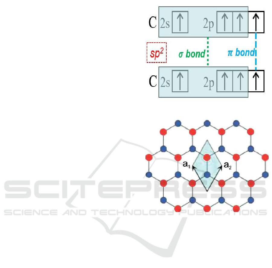
within a hexagonal lattice framework. As depicted in
the provided illustration, a single molecular crystal
structure is observed (Muthuvinayagam et al., 2023).
In the 2023 study, it was determined that each carbon
atom within graphene forms sp² hybridized orbitals
(as depicted in Figure 1). The structural integrity of
the monolayer graphene is maintained by the strong
intermolecular forces known as van der Waals
interactions.
As depicted in Figure 2, the graphene structure
formed from carbon-carbon covalent bonds
demonstrates a unique lattice arrangement. In the
cell’s internal structure, the carbon atoms A and B are
positioned such that they are not aligned directly with
one another, thereby creating two separate triangular
lattice-like two-dimensional frameworks.
Figure 1: Carbon hybrid track (Original)
Figure 2: Graphene layer network (Biro, Nemes-Incze, and
Lambin, 2012)
Note: the light blue highlighted area represents the
cell, which is represented by vectors a1 and a2. It
contains two atoms from sublattice a (blue) and b
(red)
Graphene has a unique electronic structure and
electrical properties. By applying gate voltage and
other means, it is possible to induce the conductivity
of electrons or holes in graphene (where holes
represent a loss of electrons with positive charge),
which is like the conductive phenomenon in
Semiconductors (Katznelson, 2007). However, due to
its special electronic structure, unlike
semiconductors, graphene has no insulating state,
which gives it higher conductivity and makes not
sensitive to changes in the external environment.
Due to the extremely thin monolayer structure of
graphene, it is almost transparent, so it can absorb
more incident light in a wide band range (Bonaccorso
et al. 2010). Due to these inherent characteristics,
graphene has a significantly lower electronic
IAMPA 2025 - The International Conference on Innovations in Applied Mathematics, Physics, and Astronomy
504

transition energy threshold, which can efficiently use
incident photons and generate photocurrent, making
graphene have significant advantages in the
application of high-performance optoelectronic
devices.
2.2 Preparation of Graphene by CVD
To obtain graphene with high conductivity, chemical
vapor deposition (CVD) is a preferred method. The
principle is achieved by cracking carbon sources
(such as methane and ethylene) (Gong et al. 2021).
The growth mechanism can be divided into two types,
which depend on the solubility of the metal substrate
in carbon. When the solubility is high, the
carburization-decarburization mechanism can be
used (at high temperature, carbon atoms penetrate the
metal substrate and then diffuse to the metal surface
through rapid cooling, thus forming a graphene
layer). On the contrary, the surface growth
mechanism can be used (at high temperature, carbon
atoms are pyrolyzed from a gaseous carbon source
and adsorbed on the metal surface, and finally form a
continuous graphene film) (Losurdo et al. 2011).
2.3 Photoelectric Conversion Efficiency
of Graphene
Graphene plays an important role in batteries,
especially in energy storage, ion loading, and
transport. Graphene can not only be used as an active
material and catalyst in lithium battery slurry but also
plays an important role in organic solar cells (OSCs).
The electrodes of OSCs need to be highly
transparent and conductive. Therefore, transparent
conductive electrodes need to achieve the best
balance between transparency (T) and conductivity
(σ) (Li et al. 2008). This balance can be achieved by
the following formula:
𝑇 = (1 + [𝑀
/2𝑅𝑠][𝑋
/𝑋
])
(1)
Of which,𝑀
is free space impedance,𝑋
and
𝑋
represent optical conductivity and two-
dimensional conductivity, respectively. The
resistance Rs is proportional to the number of layers
(n), which can be figured up by the following
formula: 𝑅𝑠 = (𝑛𝑋
)
(Sun et al., 2015).
According to this formula, graphene can be
modified and doped to optimize its performance.
When the n is around 4, a better balance between
transparency and conductivity can be achieved
(Mahmoudi, Wang, and Hahn, 2018). This makes
graphene more advantageous than other materials in
the market.
3 HETEROSTRUCTURE OF
GRAPHENE AND OTHER
MATERIALS
3.1 Concept of Two-Dimensional
Structure and Two-Dimensional
Heterostructure of Graphene
3.1.1 Two-Dimensional Structure
Graphene is a type of two-dimensional layered
material (2DLMs), where each layer consists of a
two-dimensional lattice formed by covalently bonded
carbon atoms. It is worth noting that the neighbouring
layers are physically linked through relatively weak
intermolecular forces known as van der Waals
interactions, which play a critical role in determining
their structural integrity and overall behaviour (Yi et
al. 2019). These intrinsic properties form the
cornerstone upon which the surface behaviour and
heterostructure formation are built.
The charge carriers within graphene operate with
an intrinsic massless nature and exhibit extraordinary
mobility, which significantly enhances their transport
properties. Quantum Hall Effect (QHE) has recently
demonstrated remarkable potential to be observed at
temperatures that surpass conventional limits, with
recent experimental results indicating feasibility even
near room temperature.
By utilizing the framework of density functional
theory (DFT), recent research by a team of scientists
has demonstrated that when water droplets are
physically adsorbed onto the surface of graphene,
they significantly alter its electrical characteristics
(Taherian et al., 2013). The findings indicate that
graphene exhibits a notable level of hydrophobic
properties, which suggests it effectively repels water.
The hydrogen bonds within water molecules in liquid
droplets are significantly stronger than the energy
required to adsorb these molecules onto a single-layer
graphene surface. As a result, its influence on the
electrical characteristics of graphene is minimal. The
recent findings demonstrate that graphene’s unique
properties make it an exceptional candidate for
protecting different substrate surfaces while
simultaneously maintaining their inherent wettability
characteristics. The surface characteristics of these
materials play a pivotal role in the development of
graphene-based composites and optoelectronic
devices, as highlighted by the research (Dai, Wang,
and Wu, 2016).
3.1.2 Introduction of Heterostructure
In optoelectronic devices, graphene alone cannot
achieve all functions, but by forming a
Graphene Two-Dimensional Heterostructure and Its Application in High-Efficiency Optoelectronic Devices
505
heterostructure with other materials, it can achieve
functions that a single material cannot achieve. In
2010, Dean and other scientists proved that hexagonal
boron nitride (hBN) can be used as an ideal two-
dimensional substrate material for graphene, because
hBN has excellent electrical insulation, excellent
thermal conductivity and excellent lubrication
performance (Wang et al. 2014).
The vertical stacking of graphene and hBN can be
achieved by van der Waals forces. However, if the
transverse connection structure is to be formed, the
manufacturing process will be more complex. To
obtain shape-controllable graphene hexagonal boron
nitride (G-hBN) heterostructures, a method has been
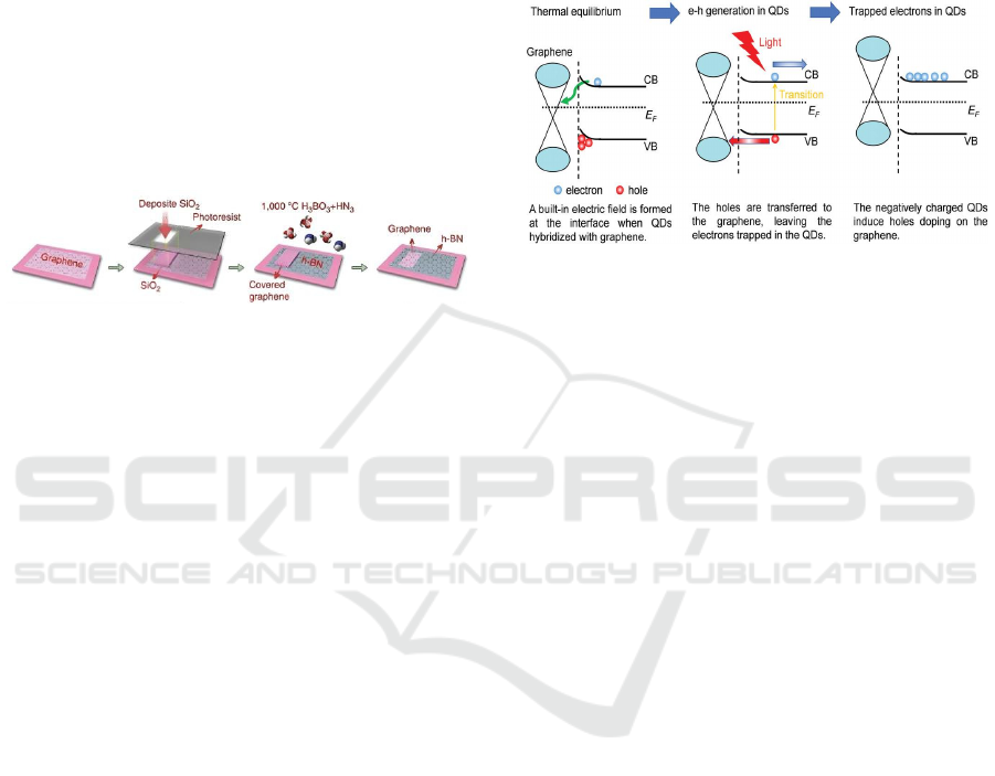
proposed, as shown in Figure 3.
Figure 3: Shape-controlled transverse g-hBN
heterostructure fabrication: the conversion process of
spatial control (Li et al., 2009)
Graphene hBN heterostructure can be obtained by
covering the required graphene region with silica,
using boric acid as a boron source and ammonia as a
nitrogen source to convert G-hBN at high
temperature. Because graphene has high carrier
mobility, it can quickly absorb the generated
photoelectrons and control the conductive polarity of
the storage unit in the device, which makes it of great
significance in the application of photodetectors and
solar cells (Wang et al., 2014).
3.2 Graphene Heterostructure
Although the zero band gap semiconductor properties
make graphene have ideal photoelectric properties, its
optical absorption is low, only about 2.3%. To
overcome this limitation, it has become a widely used
strategy to form a heterostructure between quantum
dots (QDs), a material with excellent optical
absorption properties, and graphene (Gan et al. 2012).
As shown in Figure 4, when the quantum dot is
hybridized with neutral graphene, electrons are
transferred from the quantum dot to graphene,
thereby generating a built-in electric field at the
graphene/quantum dot interface (Song et al. 2015).
Under illumination, quantum dots absorb light and
generate electron-hole pairs, which are separated at
the graphene/quantum dot interface. The built-in
electric field transfers holes to graphene, while
retaining electrons in quantum dots.
The strong and tunable light absorption
characteristics in the quantum dot layer can
effectively generate and transfer charges to graphene.
Thanks to the high charge mobility of graphene, these
1V rw111charges can be circulated in graphene many
times, which significantly improves the photoelectric
conversion efficiency of devices (Konstantatos et al.
2012).
Figure 4: Energy level diagram of graphene/quantum dot
interface (Konstantatos et al., 2012)
As shown in Figure 4, quantum dots (QDs) can
enhance the scattering and absorption of incident
light, so they can effectively improve the response
current and responsivity of photodetectors.
Additionally, the graphene/quantum dot
heterostructure can significantly improve the
performance of the visible light detector. Graphene-
based photodetectors can be divided into three types
according to their response spectral range: ultraviolet
photodetectors, visible photodetectors, and infrared
photodetectors. Graphene/quantum dot
heterostructures have unique advantages, which can
combine the strong light absorption ability and
quantum effect of quantum dots with the high charge
mobility of graphene. This combination plays an
important role in achieving high response and
detection. The performance of photodetectors and
organic solar cells (OSC) can be further optimized by
treating the surface of quantum dots, effectively
doping quantum dots, and adjusting the size of
quantum dots.
4 APPLICATIONS OF
GRAPHENE IN THE
OPTOELECTRONIC FIELD
4.1 Graphene as a Transparent
Electrode
Indium tin oxide (ITO) remains the predominant
transparent electrode employed in photovoltaic
IAMPA 2025 - The International Conference on Innovations in Applied Mathematics, Physics, and Astronomy
506

devices due to its favourable photoelectric
characteristics, notwithstanding challenges such as
limited indium availability, mechanical fragility, and
chemical instability. (Lagerwall & Scalia, 2012).
Graphene has mechanical flexibility, rich resources,
and excellent photoelectric performance, which
perfectly makes up for the shortcomings of ITO,
improves the durability and stability of devices, and
reduces the cost.
In 2020, Koo et al. (2022) Introduced a novel form
of transparent electrode integrating polyimide and
CVD graphene, which has excellent conductivity and
mechanical stability, and achieved high efficiency
(15.2% PCE) close to traditional rigid devices in
flexible organic solar cells. In 2024, Bourahla et al.
Optimized graphene/ITO composite electrode by
introducing silver nanowires (Bourahla et al., 2024),
which significantly improved the charge transfer
ability, reduced the resistance, and maintained high
transmittance, showing good device adaptability.
Fang et al. Introduced silver-doped graphene
electrode structure into micro light-emitting diodes
(Fang et al., 2025), which effectively improved the
radiation efficiency and device performance. These
studies further verified the potential of graphene in a
new generation of flexible and high-performance
optoelectronic devices.
In summary, graphene has made major
advancements in transparent electrode materials in
recent years. By combining with PI, Ag NW, and
ITO, researchers have effectively overcome the
shortcomings of traditional ITO electrodes in
mechanical stability, chemical durability, and
resource sustainability. Graphene electrode shows
excellent photoelectric performance and application
potential in the fields of flexible optoelectronic
devices, heterojunction solar cells, and μ led. In the
future, further optimizing the preparation process of
graphene electrodes and improving their interface
engineering and charge transfer characteristics will
provide strong support to facilitate the fabrication of
high-performance and reliable next-generation
optoelectronic devices
4.2 Role of Graphene in Charge
Carrier Transport
Graphene plays an important role in boosting the
performance of solar cells by leveraging its ultra-high
carrier mobility, two-dimensional structure, and
excellent electrical properties. As an electrode or
transport layer, it can significantly accelerate charge
transmission, reduce resistance loss, and improve
current density. By constructing a heterojunction with
semiconductor materials, it can effectively enhance
charge separation efficiency and inhibit composite
loss. The out-of-plane π bonds establish weak yet
essential interactions between graphene layers
through the overlap of π electrons oriented
perpendicular to the graphene plane. These
interactions facilitate the delocalization of π
electrons, forming a cross-layer delocalization
network or electron array, which significantly
enhances the conductivity of electrons. The highly
delocalized π - π conjugate network in graphene not
only gives the material excellent conductivity but also
provides an ideal transmission path for charge
concentration, which further improves the charge
collection efficiency (Yi et al., 2020). Pure graphene
exhibits a zero-energy band structure. Upon doping,
its energy band will open. Graphene optimizes its
energy level matching through interface engineering
and chemical doping, to reduce the charge
transmission barrier, and reduce the composite loss
caused by temperature rise by using its excellent
thermal conductivity (Jiang et al., 2021).
Heteroatom doping has been demonstrated to be
the most effective method to control the band gap
engineering, optical phenomenon management, and
structural characteristics adjustment in graphene,
opening new possibilities for nano-optoelectronic
applications, especially in energy-related devices
(Sheng et al., 2011). These characteristics enable
graphene to show significant efficiency improvement
potential in perovskite solar cells, organic solar cells,
dye-sensitized solar cells, and other devices. By
further optimizing the interface modification, doping
process, and material composite strategy of graphene,
graphene is expected to assume a more vital role in
the development of efficient and stable next-
generation solar cells.
4.3 Improvement Strategies for
Graphene/Light-Absorbing Layer
Heterostructures
Graphene heterostructures have various types,
including van der Waals heterostructures, p-n
junctions, and hetero band docking structures,
showing high electron mobility, adjustable band gap,
and excellent thermal conductivity, which have a
wide range of applications.
Niu et al. Proposed a new type of heterostructure,
which uses the multilayer stacking mode of
BN/graphene monolayer/BN and BN/WSe ɑ/
ɑ/graphene monolayer/WSe ɑ/bn. Among them,
WSE ɑ, as a typical transition metal disulfide, has
excellent electrical and optical properties, and can
Graphene Two-Dimensional Heterostructure and Its Application in High-Efficiency Optoelectronic Devices
507

effectively shield the superlattice effect, which is
often affected by periodic potential disturbance
caused by lattice mismatch or interlayer torsion angle.
Through the encapsulation of WSE ɑ, the interaction
between electrons in graphene is significantly
enhanced, thus stimulating a stronger electron
correlation effect. The study further reveals that the
non-centrosymmetric stacking of boron nitride (BN)
layers leads to sliding ferroelectricity in the
heterostructure. This is a spontaneous polarization
behaviour caused by the relative slip between atomic
layers, which is reversible and directionally
controllable. In single-layer graphene devices, this
sliding ferroelectricity makes the charge polarization
switching more robust, and also provides greater
flexibility for the selection of material systems,
offering a novel design approach for the construction
of stable and efficient graphene optoelectronic
devices.
Naderi and Ahmad (2023) significantly improved
the thermal stability and photoelectric performance of
the device by introducing a graphene oxide (RGO)
layer into ZnO-based solar cells. As a graphene-
derived material with good conductivity and high
chemical stability, RGO plays an effective protective
role in the device structure. Electrophoretic
deposition technology is used in this study, which is
a process of uniformly depositing charged particles
on the substrate surface by applying an external
electric field. RGO layer is introduced upon the
surface of ZnO nanorods, which improves the
adaptability of the device to high high-temperature
environment. Experiments show that RGO can fill the
oxygen vacancy defects commonly existing in ZnO,
which usually reduce the optical stability of the
material. After the introduction of RGO, the device
showed a slower decline in efficiency at high
temperatures, which further verified the unique
advantages of graphene materials in improving the
durability of optoelectronic devices.
In general, graphene/light absorbing layer
heterostructure shows great potential in improving
the optical absorption, carrier transport, and stability
of optoelectronic devices. Researchers have
significantly improved the efficiency of solar cells,
photocatalytic systems, and photodetectors
incorporating graphene through innovative design of
heterostructures, interface engineering optimization,
and material doping. In the future, further exploring
the synergy mechanism of graphene in
multifunctional heterojunction structures and
optimizing its integration strategy with other 2D
materials will provide a broader research space for the
construction of efficient and stable optoelectronic
devices.
5 CONCLUSION
This paper reviews the research progress of two-
dimensional heterogeneous optoelectronic devices
based on graphene. Graphene synthesis methods,
preparation costs, and large-scale manufacturing
challenges are the research focus. CVD is suitable for
industrialization, but the process is complex, and the
cost is high. The redox process has a low cost and
high yield, but RGO has defects. High-quality
graphene can be prepared by the epitaxial growth
method, but the cost is high and depends on the SiC
substrate. The performance optimization and stability
of graphene in optoelectronic devices are key.
Although graphene is conductive, transparent, and
flexible, its stability is affected by the environment.
The optimization strategy includes surface
functionalization, doping technology, and packaging
process. These improvements contribute to the
application of graphene in photovoltaic cells,
photodetectors, LEDs, etc.
The research directions of graphene
optoelectronic devices include using artificial
intelligence to accelerate material screening and
performance prediction, developing ultra-fast
optoelectronic devices based on graphene, and
improving optoelectronic performance through three-
dimensional structure design. To promote the
industrialization of graphene materials, it is necessary
to develop low-cost, high-efficiency, and
environment-friendly synthesis processes, and
optimize the uniformity, stability, and controllability
of materials. Combined with multidisciplinary
means, the application of graphene in intelligent
optoelectronic systems, flexible wearable devices,
and ultrafast optoelectronic devices will bring new
breakthroughs in optoelectronic technology.
AUTHORS CONTRIBUTION
All the authors contributed equally and their
names were listed in alphabetical order.
IAMPA 2025 - The International Conference on Innovations in Applied Mathematics, Physics, and Astronomy
508

REFERENCES
Bonaccorso F, Sun Z, Hasan T, Ferrari AC. 2010. Graphene
photonics and optoelectronics. Nature Photonics
4(9):611–622.
Bourahla H, Fernández S, Ryu YK, Velasco A, Malkia C,
Boscá A, Gómez-Mancebo MB, Calle F, Martinez J.
2025. High-performance Ag-NWs doped
graphene/ITO hybrid transparent conductive electrode.
Micromachines 16(2): Article 2.
Dai J, Wang G, Wu C. 2016. Progress in surface properties
and the surface testing of graphene. Conference Paper.
Fang A, Li Q, Liu J, Du Z, Tang P, Xu H, Xie Y, Song J,
Zhang K, Yang T, Yan Q, Guo W, Sun J. 2025.
Enhanced light emission of micro LEDs using
graphene-connected micropillar structures and Ag/SiO₂
nanoparticles. ACS Photonics 12(3):1342–1350.
Gan X, Mak KF, Gao Y, You Y, Hatami F, Hone J, Heinz
TF, Englund D. 2012. Strong enhancement of light–
matter interaction in graphene coupled to a photonic
crystal nanocavity. Nano Letters 12(11):5626–5631.
Gong K, Hu J, Cui N, Xue Y, Li L, Long G, Lin S. 2021.
The roles of graphene and its derivatives in perovskite
solar cells: A review. Materials & Design 211:110170.
Jiang M, Zhang W, Zhao K, Guan F, Wang Y. 2021.
Investigations on the electronic structure and optical
properties of (Ga,N,Ga–N) doped graphene by first-
principle calculations. International Journal of Modern
Physics B 35(05):2150067.
Konstantatos G, Badioli M, Gaudreau L, Osmond J,
Bernechea M, de Arquer FPG, Gatti F, Koppens FHL.
2012. Hybrid graphene–quantum dot phototransistors
with ultrahigh gain. Nature Nanotechnology 7(6):363–
368.
Koo D, Jung S, Seo J, Jeong G, Choi Y, Lee J, Lee SM, Cho
Y, Jeong M, Lee J, Oh J, Yang C, Park H. 2020.
Flexible organic solar cells over 15% efficiency with
polyimide-integrated graphene electrodes. Joule
4(5):1021–1034.
Lagerwall JPF, Scalia G. 2012. A new era for liquid crystal
research: Applications of liquid crystals in soft matter
nano-, bio- and microtechnology. Current Applied
Physics 12(6):1387–1412.
Li X, Cai W, Colombo L, Ruoff RS. 2009. Evolution of
graphene growth on Cu and Ni studied by carbon
isotope labeling. Nano Letters 9(12):4268–4272.
Li X, Zhang G, Bai X, Sun X, Wang X, Wang E, Dai H.
2008. Highly conducting graphene sheets and
Langmuir–Blodgett films. Nature Nanotechnology
3(9):538–542.
Losurdo M, Giangregorio MM, Capezzuto P, Bruno G.
2011. Graphene CVD growth on copper and nickel:
Role of hydrogen in kinetics and structure. Physical
Chemistry Chemical Physics 13(46):20836–20843.
Mahmoudi T, Wang Y, Hahn YB. 2018. Graphene and its
derivatives for solar cells application. Nano Energy
47:51–65.
Muthuvinayagam M, Ashok Kumar SS, Ramesh K,
Ramesh S. 2023. Introduction of graphene: The
“mother” of all carbon allotropes. In: Subramaniam RT,
Kasi R, Bashir S, Ashok Kumar SS (eds). Graphene.
Springer.
Naderi N, Ahmad H. 2023. Graphene capping layer for
improving the photovoltaic stability of ZnO nanorods
solar cells under temperature variations. Optics
Communications 547:129842.
Niu R, Li Z, Han X, Qu Z, Liu Q, Wang Z, Han C, Wang
C, Wu Y, Yang C, Lv M, Yang K, Watanabe K,
Taniguchi T, Liu K, Mao J, Shi W, Che R, Zhou W, Lu
J. 2025. Ferroelectricity with concomitant Coulomb
screening in van der Waals heterostructures. Nature
Nanotechnology 1–7.
Sheng ZH, Gao HL, Bao WJ, Wang FB, Xia XH. 2011.
Synthesis of boron doped graphene for oxygen
reduction reaction in fuel cells. Journal of Materials
Chemistry 22(2):390–395.
Song Y, Li X, Mackin C, Zhang X, Fang W, Palacios T,
Zhu H, Kong J. 2015. Role of interfacial oxide in high-
efficiency graphene–silicon Schottky barrier solar cells.
Nano Letters 15(3):2104–2110.
Sun Y, Zhang W, Chi H, Liu Y, Hou CL, Fang D. 2015.
Recent development of graphene materials applied in
polymer solar cells. Renewable and Sustainable Energy
Reviews 43:973–980.
Taherian F, Marcon V, van der Vegt NFA, Leroy F. 2013.
What is the contact angle of water on graphene?
Langmuir 29(5):1457–1465.
Wang H, Liu F, Fu W, Fang Z, Zhou W, Liu Z. 2014. Two-
dimensional heterostructures: Fabrication,
characterization, and application. Nanoscale
6(21):12250–12272.
Yi J, Choe G, Park J, Lee JY. 2020. Graphene oxide-
incorporated hydrogels for biomedical applications.
Polymer Journal 52(8):823–837.
Yi Y, Chen Z, Yu XF, Song J. 2019. Recent advances in
quantum effects of 2D materials. Advanced Quantum
Technologies 2(5–6):1800111.
Graphene Two-Dimensional Heterostructure and Its Application in High-Efficiency Optoelectronic Devices
509
