
Progress and Prospects of Topological Materials in Photodetection
Yunna Duan
a
Department of Physics, Southern University of Science and Technology, Shenzhen, Guangdong, China
Keywords: Topological Materials, Photodetection, Photoelectric Conversion.
Abstract: Topological materials exhibit unique electronic properties, making them promising for photodetection. This
paper presents a comprehensive review of the emerging applications of topological materials in
photodetection, focusing on their exceptional electronic properties that enable superior device performance.
The article briefly explains the transport mechanisms of topological insulators, topological semimetals,
topological superconductors, as well as new types of topological materials such as chiral topological materials
and ferroelectric topological materials.The article also systematically examines recent breakthroughs
demonstrating how these materials achieve remarkable photodetection capabilities through enhanced
responsivity, improved detectivity, and ultrafast response times. The paper discusses promising
implementation scenarios across multiple technological domains, particularly in high-speed optical
communications, advanced infrared imaging systems, and next-generation quantum devices. Although
challenges persist in material synthesis and device integration, topological photodetectors represent a
transformative advancement in optoelectronics, offering unprecedented combinations of broadband
sensitivity, rapid response, and robust performance that could redefine detection technologies across scientific
and industrial applications.
1 INTRODUCTION
Photodetectors have significant applications in
various fields such as optical communication,
imaging, security monitoring, and biosensing (Liang
et al., 2018). Research indicates that topological
materials can detect in the range from infrared to
terahertz waves, breaking through the limitations of
traditional detection materials. They also possess high
responsivity, response time, and a high signal-to-
noise ratio. These properties can be further enhanced
through structural designs such as doping, nanowires,
and heterojunctions, as well as using strain and other
control methods. Moreover, with the increasing
discovery of topological materials and the continuous
progress in their preparation techniques, the
application of topological materials in photoelectric
detection will have greater potential.
This article aims to systematically explore the
unique advantages, performance regulation methods,
device design strategies, and application potential of
topological materials in the field of photoelectric
detection, providing a research foundation for the
a
https://orcid.org/0009-0004-6641-7404
development of a new generation of high-
performance photoelectric detectors.
2 OVERVIEW OF
TOPOLOGICAL MATERIALS
Topological materials exhibit unique electronic
properties due to their special surface states. They are
mainly classified into four types as topological
insulator (TI), topological crystalline insulator (TCI),
topological semimetal (TSM), and topological
superconductor (TSC).
TIs are bulk insulating but with conductive
surface states protected by time reversal symmetry,
enabling high carrier mobility.
TCIs have surface states protected by crystal
symmetries such as mirror symmetry, as seen in
SnTe. They show insulating bulk and conductive
edges, suitable for photodetection.
TSMs feature bulk band crossing (Dirac/Weyl
points) near the Fermi level, leading to high carrier
concentration and mobility. Examples include TaAs
Duan, Y.
Progress and Prospects of Topological Materials in Photodetection.
DOI: 10.5220/0013827500004708
Paper published under CC license (CC BY-NC-ND 4.0)
In Proceedings of the 2nd International Conference on Innovations in Applied Mathematics, Physics, and Astronomy (IAMPA 2025), pages 457-463
ISBN: 978-989-758-774-0
Proceedings Copyright © 2025 by SCITEPRESS – Science and Technology Publications, Lda.
457

(Weyl) and Na₃Bi (Dirac), ideal for low-power, high-
sensitivity photodetectors.
TSCs host Majorana zero-energy modes on
surfaces, with robust, defect-resistant conduction
channels. Their combination of superconductivity
and topological protection is valuable for energy-
efficient devices.
Moreover, some materials cannot be classified
within the traditional topological phase framework.
These are referred to as new topological phases,
including topological chiral crystals and ferroelectric
topological materials.
Topological chiral crystals lack mirror symmetry
in their lattice structure and display topological
behaviors even without symmetry protection. In some
cases, they resemble topological semimetals,
especially when band crossing points (such as Dirac
or Weyl points) appear near the Fermi surface,
offering potential for broad-spectrum photodetection.
Topological ferroelectric materials share features
of both topological insulators and superconductors,
making them highly promising for photoelectric
detection applications.
3 PHOTODETECTOR:
PRINCIPLES,
MANUFACTURING PROCESS,
AND STRUCTURES
3.1 Principle
Topological materials demonstrate exceptional
photodetection properties owing to their unique band
structures, such as surface states and linear
dispersion, enabling strong light absorption,
particularly in the IR and THz regions. Their high
carrier mobility and low scattering rates facilitate
rapid charge transport with minimal recombination
losses, while topological protection further enhances
carrier stability. Moreover, the surface states
significantly enhance photocurrent generation, even
under low-energy excitation, thereby improving both
sensitivity and response speed in photodetectors.
In addition to these mechanisms, studies have
shown that doping with magnetic elements can break
the time-reversal symmetry of the surface states in
topological insulators, thereby inducing a band gap in
these states. Consequently, the band gap of
topological insulator surface states can be effectively
controlled through the introduction of magnetic
impurities
(Swatek et al., 2020). Studies have also
demonstrated that strain can influence the optical
absorption of topological insulator films by altering
crystal symmetry or modulating the band gap of
surface states. Such strain-induced regulation, rather
than changes in film thickness, enables precise
control at the device level, facilitating efficient
photoelectric detection across a broad photon energy
range. Furthermore, this approach can enhance the
previously reported anisotropic photoelectric current
response, offering new opportunities for the
development of advanced photodetectors (Brems et
al., 2018).
3.2 Manufacturing Process and
Structures
Preparation of transport devices using topological
materials primarily involves two methods: thin film
growth and heterostructure construction. Thin film
growth utilizes molecular beam epitaxy (MBE) for
high-quality single-crystal films with precise doping
control. Chemical vapor deposition (CVD) produces
large-area 2D materials but requires a transfer step.
Electrochemical deposition and radio frequency
magnetron sputtering directly grow films on
substrates, avoiding interface contamination. The
hydrothermal method is cost-effective for multi-
dimensional heterojunctions.
Heterostructure construction relies on van der
Waals stacking, where interfaces are formed without
chemical bonds via mechanical transfer, and vertical
epitaxial growth for direct contact. In situ insertion of
passivation layers optimizes Schottky junction
performance.
Device design focuses on performance. Back-to-
back heterojunctions suppress dark current through
dual interfaces, improving the signal-to-noise ratio.
Self-powered p-n junctions operate at zero bias using
built-in electric fields. Schottky junctions combine
passivation layers to enhance response speed (160 ns)
and band coverage (up to 10.6 μm). Photochemical
cells separate charge carriers via a solid-liquid
interface electric field without external bias. Special
structures like plasma antenna coupling enhance
terahertz absorption, while topological lasers enable
room-temperature lasing, and topological photonic
crystal modulators support ultra-high-speed signal
transmission.
Material preparation is shifting from traditional
mechanical exfoliation to in-situ growth methods to
reduce interface defects and improve process
compatibility. Device design is embracing multi-
dimensional heterojunctions and self-powered
structures, with a clear trend toward functional
integration. Future challenges include achieving
IAMPA 2025 - The International Conference on Innovations in Applied Mathematics, Physics, and Astronomy
458
large-scale uniform growth techniques, precise
control of interface states and defects, and deep
integration with existing semiconductor processes
(CMOS, photonic integrated circuits).
4 RESEARCH PROGRESS IN
RECENT YEARS
4.1 The Application of Topological
Insulators in Photodetection
In the field of topological insulators, Wang et al.
(2023) combined transition metal dichalcogenide
(MoS₂) with a topological insulator (Sb₂Te₃) to create
a self-powered broadband photodetector, addressing
the severe recombination issue at the interface of
traditional 2D material heterojunctions. The device
demonstrated record-low dark current (2.4 pA) and
high responsivity (>150 mA/W) in the 500-900 nm
wavelength range, offering a new solution for low-
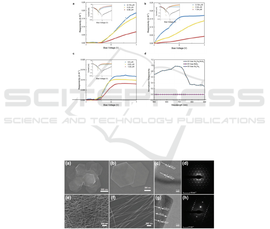
power optoelectronic integration (Figure 1).
Figure 1: Electrical characterization of Sb2Te3/MoS2 PN junction heterostructure photodetector (Wang et al., 2013)
In the same year, Zhao et al. innovatively
proposed a 1D p-Te/2D n-Bi₂Te₃ multidimensional
heterojunction structure, fabricated via a
hydrothermal method. The device achieved a high on-
off ratio (377.45) and excellent stability (only an
18.08% decay over 30 days) in the 365-850 nm
wavelength range, filling the technological gap for
low-cost, high-performance self-driven
photodetectors (Figure 2) (Zhao et al., 2023).
Figure 2: SEM images of Bi2Te3 NSs with different magnifications (Zhao et al., 2023)
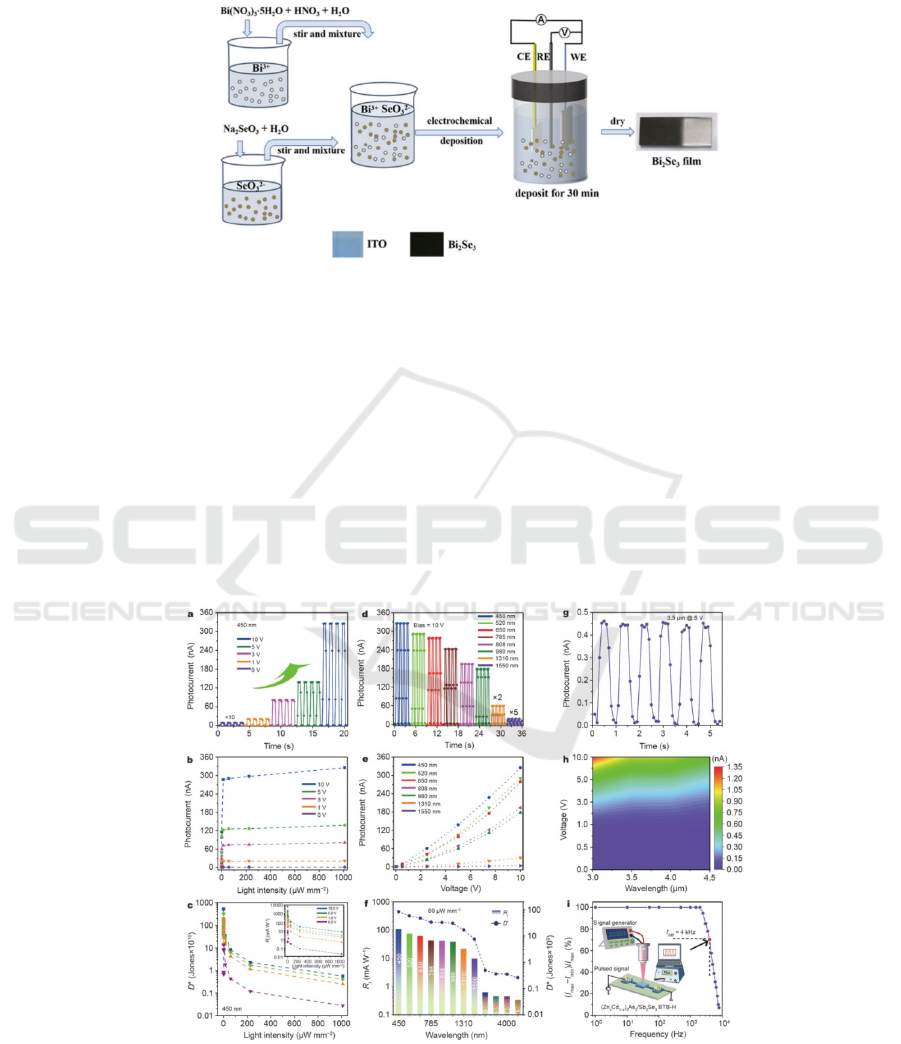
In 2024, Ye et al. pioneered the direct
electrodeposition of Bi₂Se₃ films on ITO, avoiding
interface contamination caused by traditional transfer
methods. The resulting photoelectrochemical
detector achieved a photocurrent density of 2.87
μA/cm², with significantly improved stability (88%
retention after one week), opening a new path for
large-scale fabrication of topological insulator films
(Ye et al., 2024). In the same year, the Maurya team
first combined TIBiSe₂ with GaN to construct a
Progress and Prospects of Topological Materials in Photodetection
459
vertical heterojunction diode, achieving high-
responsivity detection in the ultraviolet to near-
infrared (300-900nm) wavelength range. The device
exhibited a rectification ratio of 160, overcoming the
limitations of traditional broadband detectors that rely
on complex band engineering
(Figure 3) (Maurya et
al., 2024).
Figure 3: The preparation process of Bi2Se3 film (Ye et al., 2024)
Recent studies on topological insulators have made
progress in the design optimization of heterostructure,
innovation of fabrication processes, and improvement
of device performance. These related research efforts
have facilitated breakthroughs in wide-spectrum
response, self-powered operation, high sensitivity,
and long-term stability of devices, providing new
solutions and development paths for achieving high-
performance, low-cost, and integrated photodetection
technologies.
4.2 The Application of Topological
Semimetals in Photodetection
In the field of topological semimetals, Zhang et al.
(2022) first designed and fabricated a back-to-back
heterojunction photodetector based on the three-
dimensional Dirac semimetal (Cd₁₋ₓZnₓ)₃As₂. The
dual-heterojunction structure suppressed the dark
current to the picoampere level, achieving a signal-to-
noise ratio as high as 10⁴. This device simultaneously
optimized broadband detection (450 nm–4.5 μm) and
ultrafast response (87.5 μs), offering a new
architecture for infrared focal plane arrays.
Figure 4: Photodetection performance of the (Cd1-xZnx) As2/Sb2Se3 BTB heterojunction (Zhang et al., 2022)
In 2023, the Lin Wang team innovatively utilized
the topological band characteristics of the Dirac
semimetal PtSe₂, combined with a nanoplasmonic
antenna, to achieve high responsivity (0.2 A/W) and
IAMPA 2025 - The International Conference on Innovations in Applied Mathematics, Physics, and Astronomy
460
picosecond-level response in the terahertz (THz)
range (<1.24 meV) at room temperature. This
breakthrough surpassed the performance limits of
traditional semiconductor materials in low-energy
photon detection (Figures 4, 5)(Wang et al., 2022).
Figure 5: Characteristics of the PtSe2 low-energy photon detector (Wang et al., 2022)
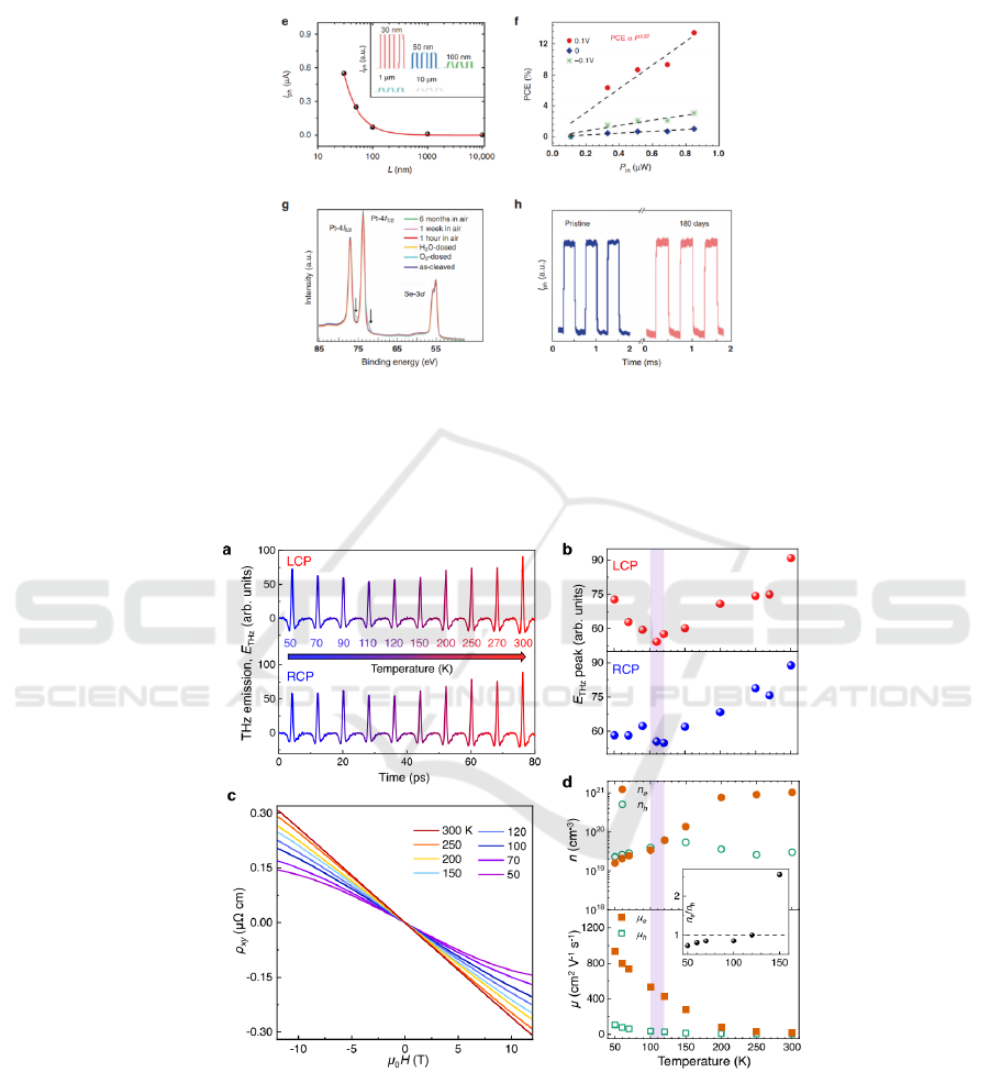
In 2024, Li et al. first observed the strong coupling
effect between spin-polarized electrons and phonons
in PtTe₂ using ultrafast spectroscopy, revealing the
microscopic mechanism of anisotropic phonon
dynamics. This study laid the theoretical foundation
for the application of topological materials in ultrafast
optoelectronic devices (Figure 6)
(Li et al., 2024).
Figure 6: Temperature-dependent THz emission and its correlation with carrier compensation (Li et al., 2024)
Topological semimetals have made significant
progress in the field of photoelectric detection,
manifested in aspects such as wide-spectrum high
response, ultrafast response speed, low dark current,
and unique spin-phonon coupling mechanism,
providing new material systems and theoretical
foundations for the development of high-performance
and ultrafast optoelectronic devices.
Progress and Prospects of Topological Materials in Photodetection
461

4.3 The Application of Topological
Superconductors in Photodetection
The Pattanayak team (2024) systematically measured
the optical constants of FeTe₀.₆Se₀.₄ topological
superconducting nanosheets in the 450-1100 nm
range and at 4K-295K. They found that in the
superconducting state (4K), the refractive index
ranged from 2.81 to 4.26, and the extinction
coefficient from 2.24 to 3.21. The material exhibited
dual-Drude multi-band characteristics and anomalous
dispersion, confirming its high extinction coefficient
outperforms traditional copper-based
superconductors, providing key parameters for the
development of quantum photonic devices like high-
temperature superconducting single-photon detectors
(Figure 7)(Pattanayak, Rout, & Jha, 2025).
Figure 7: Pump-modulated MOKE loops in the time
domain (Pattanayak, Rout, & Jha, 2025).
4.4 The Application of Novel
Topological Materials in
Photodetection
Topological handedness crystals (such as RhSi and
CoSi) and ferroelectric topological materials (such as
GeTe and SnTe) demonstrate unique advantages in
photoelectric detection. RhSi and CoSi achieve a
wide-spectrum response through the quantumized
circularly polarized photocurrent effect, and have
high sensitivity and fast response characteristics in
the terahertz to infrared wavelength range. GeTe and
SnTe utilize the synergy of ferroelectricity and
topological surface states, showing controllable high
photocurrent response rate in the mid-infrared
wavelength range. The excellence of these materials
stems from their special Berry curvature and band
structure, providing important candidate systems for
the next generation of high-performance
photoelectric detectors.
Research indicates that the photocurrent response
of CoSi at 0.4 eV photon energy reaches 550 μA/V²,
and the responsivity of SnTe at 635 nm wavelength is
as high as 49.03 A/W, which is significantly superior
to that of traditional semiconductor devices. The
efficient working characteristics of these materials
under zero bias conditions make them have important
application prospects in terahertz sensing and infrared
detection fields
(Shen et al., 2024).
As seen from the above, research on topological
materials has shifted from fundamental property
exploration to device applications. Several
achievements, such as the first realization of
broadband self-powered detection, breakthroughs in
terahertz room-temperature detection limits, and the
discovery of new mechanisms for light-controlled
magnetism, mark the maturity of this field.
5 CONCLUSIONS
Topological materials exhibit unique electronic
properties that make them highly suitable for next-
generation optoelectronic devices. In optical
communication, photodetectors based on topological
materials offer ultrafast response times and
exceptional carrier mobility, enabling high-speed
optical signal detection and transmission for data
centers and 5G/6G networks. In infrared imaging and
sensing, their broad spectral response, from
ultraviolet to terahertz, allows for versatile
applications in night vision, thermal imaging, and
biomedical sensing. Additionally, in quantum
information processing, features such as zero energy
gap and chirality enable the realization of quantum
bits and support technologies like quantum
computing and communication, highlighting their
potential in quantum photonic devices.
This review systematically examined five major
classes—topological insulators, crystalline insulators,
semimetals, superconductors, and novel topological
materials—highlighting their distinct mechanisms for
enhancing photodetector performance. Key
advantages such as ultrafast response, high
sensitivity, and low-energy consumption position
these materials as superior alternatives to
conventional semiconductors.
While significant progress has been made in
understanding these materials and developing device
architectures like heterojunctions, challenges in
large-scale synthesis and device integration remain.
Future efforts should focus on optimizing fabrication
techniques, improving material quality, and exploring
hybrid systems to overcome current limitations. With
IAMPA 2025 - The International Conference on Innovations in Applied Mathematics, Physics, and Astronomy
462

continued research, topological photodetectors could
enable breakthroughs in high-speed optical
communication, infrared imaging, and quantum
information processing. Their unique combination of
robustness and performance promises to drive
innovation in next-generation optoelectronic devices,
paving the way for transformative applications across
scientific and industrial fields.
REFERENCES
Brems, M. R., Paaske, J., Lunde, A. M., Willatzen, M.,
2018. Strain-enhanced optical absorbance of
topological insulator films. Physical Review B, 97(8).
Huang, A., Liang, F., Liang, L., Zhao, X., Luo, L., Liu, Y.,
Tong, X., 2018. A sensitive broadband (UV–vis–NIR)
perovskite photodetector using topological insulator as
electrodes. Advanced Optical Materials, 7(4).
Li, Z., Chen, Y., Song, A., Zhang, J., Zhang, R., Zhang, Z.,
Wang, X., 2024. Anisotropic phonon dynamics in Dirac
semimetal PtTe₂ thin films enabled by helicity-
dependent ultrafast light excitation. Light: Science &
Applications, 13(1).
Maurya, G. K., Gautam, V., Ahmad, F., Singh, R., Verma,
S., Kandpal, K., Kumar, P., 2024. Topological insulator
TlBiSe₂/GaN vertical heterojunction diode for high
responsive broadband UV to near-infrared
photodetector. Journal of Electronic Materials, 53(3):
1561–1576.
Pattanayak, A. K., Rout, J., Jha, P. K., 2025. Temperature-
dependent optical constants of nanometer-thin flakes of
Fe(Te,Se) superconductor in the visible and near-
infrared regime. APL Quantum, 2(1).
Shen, Y., Primeau, L., Li, J., Nguyen, T.-D., Mandrus, D.,
Lin, Y. C., Zhang, Y., 2024. Nonlinear photocurrent in
quantum materials for broadband photodetection.
Progress in Quantum Electronics, 97: 100535.
Swatek, P., Wu, Y., Wang, L.-L., Lee, K., Schrunk, B., Yan,
J., Kaminski, A., 2020. Gapless Dirac surface states in
the antiferromagnetic topological insulator MnBi₂Te₄.
Physical Review B, 101(16).
Wang, H., Dong, C., Gui, Y., Ye, J., Altaleb, S.,
Thomaschewski, M., Sorger, V. J., 2023. Self-powered
Sb₂Te₃/MoS₂ heterojunction broadband photodetector
on flexible substrate from visible to near infrared.
Nanomaterials, 13(13): 1973–1973.
Wang, L., Han, L., Guo, W., Zhang, L., Yao, C., Chen, Z.,
Lu, W., 2022. Hybrid Dirac semimetal-based
photodetector with efficient low-energy photon
harvesting. Light: Science & Applications, 11(1).
Ye, Y., Yu, R., Huang, Z., Qiao, H., Qi, X., 2024.
Photoelectrochemical photodetector based on
electrodeposited Bi₂Se₃ film with superior performance.
Applied Physics A, 130(1).
Zhang, X., Yang, Y., Zhou, H., Liu, X., Pan, R., He, Y.,
Wang, J., 2022. Three-dimensional Dirac semimetal
(Cd₁₋ₓZnₓ)₃As₂/Sb₂Se₃ back-to-back heterojunction for
fast-response broadband photodetector with ultrahigh
signal-to-noise ratio. Science China Materials, 66(4):
1484–1493.
Zhao, C., Wang, D., Cao, J., Zeng, Z., Zhang, B., Pan, J.,
Wang, J., 2023. Highly efficient 1D p-Te/2D n-Bi₂Te₃
heterojunction self-driven broadband photodetector.
Nano Research, 17(3): 1864–1874.
Progress and Prospects of Topological Materials in Photodetection
463
