
Wide Band High PSRR LDO Voltage Regulator
Laxmi Koutanali
a
, Sujata S Kotabagi, Ritu Ramesh Vernekar
b
, Vijeta D Chitragar
c
and Prajwal Sangalad
d
School of Electronics and Communication Engineering, KLE Technological University, Hubli, India
Keywords:
LDO, PSRR, Line Regulation, Load Regulation, Noise Rejection, Transient Response.
Abstract:
The design and implementation of Low Dropout Voltage Regulators (LDOs) play a critical role in the power
management of modern electronic systems. LDOs are particularly important in low-voltage and noise-sensitive
applications, such as portable devices, RF circuits, and automotive electronics. This paper presents a Wide
Band High Power Supply Rejection Ratio (PSRR) LDO, designed using UMC 180nm CMOS technology,
operating at an input voltage of 1.4V and delivering a stable output of 1+/-0.66%V. The LDO achieves superior
performance, with line regulation of 1.07 V/V, load regulation of 16.33 mV / A and a PSRR of -55.82 dB at
1 MHz and the layout design at 274.29 µm× 40.2µm (0.011026 mm
2
), the LDO arrangement is ideal for both
power and signal integrity. Simulation results confirm the LDO’s robustness in minimizing voltage spikes,
ensuring stable operation under dynamic load conditions. The high PSRR and low noise characteristics make
this LDO design ideal for sensitive analog and RF circuits, where power supply fluctuations can significantly
impact performance.
1 INTRODUCTION
The demand for power-efficient, low-noise power
management solutions has never been more critical
in today’s rapidly evolving technological landscape.
The increasing complexity of modern electronic sys-
tems ranging from smartphones and laptops to wear-
ables and medical devices has placed stringent re-
quirements on power delivery systems. To increase
battery life and give delicate electronics steady, quiet
power, these gadgets require effective power manage-
ment.
LDOs are linear regulators that provide clean,
low-noise power perfect for delicate applications like
audio, analog, and radio frequency systems. They
also guarantee a steady output voltage.LDOs are per-
fect for ADCs, sensors, and communication modules
because they minimize dropout voltage, reduce heat
waste, and prolong battery life in low-voltage appli-
cations.
One important LDO statistic that assesses its ca-
pacity to reduce input voltage variations is PSRR. A
a
https://orcid.org/0009-0007-0082-4674
b
https://orcid.org/0009-0001-5671-6556
c
https://orcid.org/0009-0005-1406-9150
d
https://orcid.org/0009-0006-3305-7961
high PSRR stops noise from influencing the output,
for instance, EMI or ripples. This is crucial for high-
precision analog circuits and radio frequency trans-
mission, where errors can be caused by power sup-
ply noise. For wideband circuits to minimize power
supply noise across a large frequency range, high
PSRR is essential. This guarantees consistent per-
formance in audio, RF, and precision instrumentation
systems. High PSRR is essential for signal integrity
since power supply fluctuations can distort signals.
Stable output and dependable operation are main-
tained using broadband op-amps and LDOs with high
PSRR. Improved PSRR at high frequencies is the goal
of recent LDO developments in order to reduce power
supply noise. Adaptive biasing and feedforward com-
pensation are two methods that enhance noise reduc-
tion. Dropout voltage and quiescent current are in-
creased when PMOS and NMOS pass components are
combined. PMOS may have a greater dropout volt-
age; however, it is preferable for low quiescent cur-
rent.
1.1 Objectives
The main objective is to create an LDO that performs
better across several important characteristics, with an
12
Koutanali, L., S Kotabagi, S., Ramesh Vernekar, R., D Chitragar, V. and Sangalad, P.
Wide Band High PSRR LDO Voltage Regulator.
DOI: 10.5220/0013607900004664
Paper published under CC license (CC BY-NC-ND 4.0)
In Proceedings of the 3rd International Conference on Futuristic Technology (INCOFT 2025) - Volume 3, pages 12-18
ISBN: 978-989-758-763-4
Proceedings Copyright © 2025 by SCITEPRESS – Science and Technology Publications, Lda.

emphasis on noise reduction, power efficiency, and
voltage regulation. The specific objectives are as fol-
lows:
• Minimize Dropout Voltage: In battery-powered
systems, the LDO’s reduce the input-output volt-
age differential, which is essential for power effi-
ciency.
• Obtain a High Power Supply Rejection Ratio
(PSRR): For the LDO to prevent power supply
noise, significant PSRR at high frequencies is nec-
essary. This keeps delicate analog and radio fre-
quency circuitry from being impacted by noise.
• Ensure Stable Output Voltage: In spite of changes
in input voltage or load current, the LDO main-
tains a steady output voltage, preserving device
dependability and performance.
2 LITERATURE SURVEY
The significance of LDOs in providing reliable and
efficient voltage supplies, especially in portable and
low-power applications, has led to their design and
development being a primary focus in power man-
agement integrated circuits (PMICs). Improved LDO
performance has resulted from recent developments
that prioritized lowering power consumption, improv-
ing transient response, and better integrating with
contemporary systems. The increasing needs for en-
ergy efficiency and dependable power for delicate
electronic equipment can be better met by LDOs
thanks to these advancements.
Enhancing the transient response is one of the
main issues with LDO design, especially when the
load current fluctuates quickly. Because the pass el-
ement cannot adapt rapidly to changes in load cir-
cumstances, traditional LDOs suffer from delayed
transient reactions. By forcing the pass transistor to
change the gate voltage more quickly, a push-pull
buffer is a popular method to improve transient re-
sponsiveness(Li et al., 2019). To increase stability
and shorten the output voltage’s settling time follow-
ing load changes, this method moves the poles and
lowers the gate capacitance.
Transient performance may be greatly improved
by using the dual-loop flipped voltage follower (FVF)
design (Wang et al., 2016). A dual-loop control mech-
anism is used in this architecture, with one loop con-
trolling the output voltage and the other concentrat-
ing on enhancing the stability of the reference volt-
age. The LDO can respond to transitory situations
with a reaction time of as little as 45 ns because of its
structure. Furthermore, noisy supply voltages might
impair system performance in situations where high
PSRR is necessary, such RFID systems. In these situ-
ations, this architecture is quite effective.
LDOs are expected to function at lower supply
voltages with greater efficiency as process technolo-
gies continue to scale down. LDOs must frequently
function at voltages as low as 1 V in modern CMOS
processes, which poses difficulties for stability and
transient responsiveness. Bandgap reference circuits
with low-temperature coefficients are used to produce
stable reference voltages across a broad temperature
range in order to overcome these issues(Tham and
Nagaraj, 1995) (Neri et al., 2015).
Reducing quiescent current in battery-powered
devices is essential for increasing battery life. In
portable electronics, where power efficiency directly
affects the device’s running duration, low quiescent
current LDO designs are crucial(Rincon-Mora and
Allen, 1998). Scientists have created low-quiescent-
current operating LDOs that maintain load manage-
ment and transient responsiveness.
With digitally controlled systems, Digital Low
Dropout Regulators (D-LDOs) provide more flexibil-
ity. They offer improved efficiency, flexibility in re-
sponse to load variations, and accurate voltage regu-
lation(Huang et al., 2016). Through adaptive control,
D-LDOs lower static power consumption and facil-
itate multi-phase designs for increased stability and
efficiency.
Hybrid Low Dropout Regulators (LDOs) merge
analog and digital regulation techniques, offering a
balance between precision and flexibility. The analog
feedback ensures accurate voltage regulation and fast
transient response, while the digital controls provide
programmability and dynamic adjustment according
to varying power demands. This combination makes
hybrid LDOs ideal for applications with fluctuating
load conditions, such as mobile processors and RF
systems, where rapid changes in load are common.
By integrating digital control with analog precision,
hybrid LDOs significantly enhance power efficiency
and transient performance, making them a key focus
in modern power management solutions.
Performance in noise-sensitive applications such
as ADCs/DACs and RF transceivers depends on min-
imizing output noise and attaining a high Power Sup-
ply Rejection Ratio (PSRR). Signal quality might be
deteriorated by voltage fluctuations brought on by low
PSRR. In order to get around this, current studies
have concentrated on sophisticated noise-reduction
and compensating strategies including ripple can-
cellation and active feedback loops, which enhance
PSRR over a broad frequency range(El-Nozahi et al.,
2010). These techniques are essential for contempo-
Wide Band High PSRR LDO Voltage Regulator
13
rary LDO designs in high-performance analog sys-
tems and are especially successful at low supply volt-
ages.
Low Dropout Regulators (LDOs) are essential in
modern electronics, particularly in applications re-
quiring low noise and high Power Supply Rejec-
tion Ratio (PSRR), such as RF transceivers and IoT
devices. Recent advancements focus on improv-
ing power efficiency and scalability through digi-
tal LDOs (D-LDOs), which offer programmability
and adaptability in dynamic environments. Hybrid
LDOs, combining analog precision with digital con-
trol, further enhance efficiency under varying load
conditions. Additionally, low-power and sub-1V
LDOs have gained attention for their ability to operate
with minimal voltage headroom, crucial for ultra-low-
power devices. Improved compensation techniques
like ripple cancellation have also enhanced PSRR,
making LDOs more effective in noise-sensitive appli-
cations(Shen et al., 2006).
Digital and hybrid architectures are examples of
LDO design advancements that prioritize noise per-
formance, scalability, and power efficiency. These
days, wide-band high-PSRR LDOs are perfect for
contemporary noise-sensitive systems because they
offer dependable voltage management and noise re-
jection.
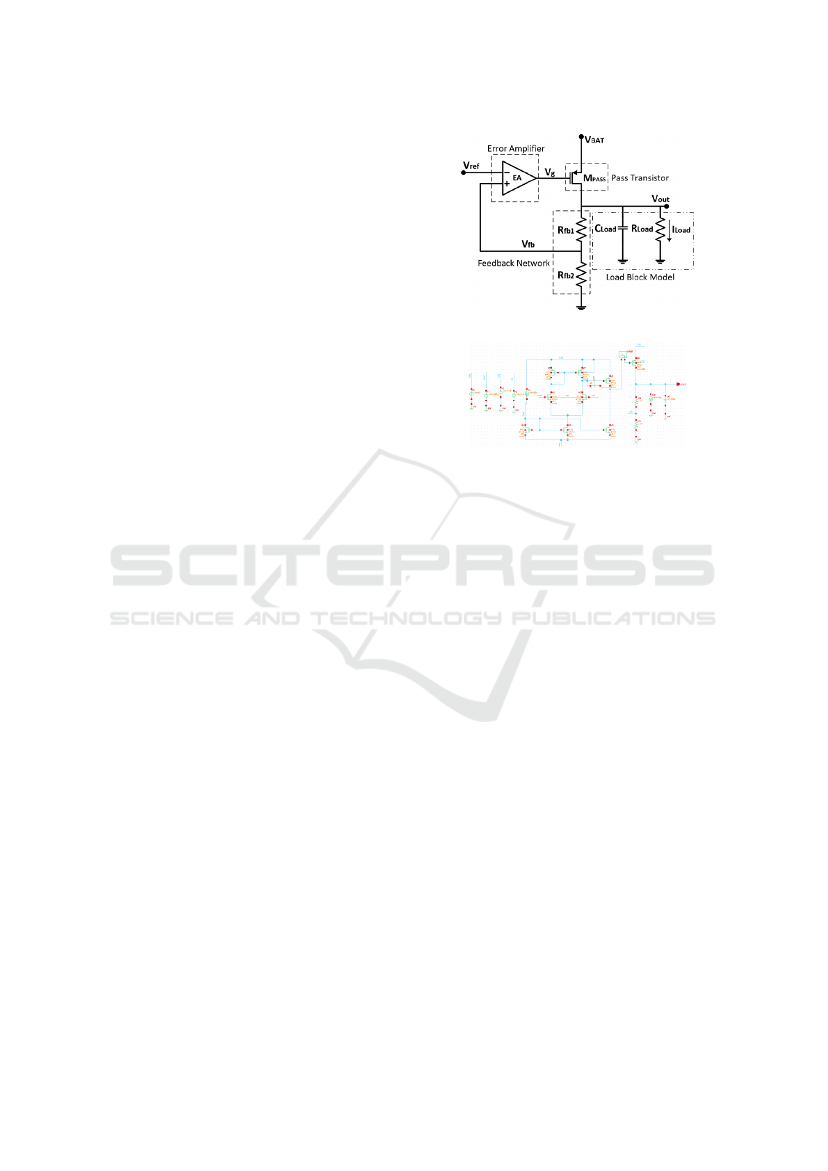
3 METHODOLOGY
A Miller compensation network for stability, a power
stage, and an error amplifier for feedback control are
all included in the suggested LDO architecture. While
maintaining low quiescent current needs, the 7-pack
error amplifier seeks to optimize gain, stability, and
power efficiency. Built using UMC 180nm technol-
ogy, it has a 1.4V input and a 1V output. It can han-
dle load currents ranging from 2 to 10 mA and a 50
µA quiescent current. The 7-pack amplifier boosts to-
tal gain and voltage headroom by using a multi-stage,
stacked construction.
This arrangement guarantees that each stage con-
tributes to the overall amplification while preserv-
ing good DC gain and stability for low-voltage, low-
power applications. The upper stages of this structure
are in charge of driving the output, making sure that
the amplifier can manage the necessary load current.
In contrast, the lower stages’ transistors are made to
handle the input signal and offer significant differ-
ential gain. The design includes a meticulous bias-
ing network to maintain the high gain necessary for
regulatory precision to guarantee that every transistor
works in the saturation zone.
Figure 1: Schematic Diagram.
Figure 2: Schematic Diagram.
The biasing system must be ultra-low power, us-
ing current mirrors operation to lower power con-
sumption without sacrificing performance, given the
50 µA quiescent current limitation fig[2]. The 7-pack
structure’s cascading techniques enhance the output
impedance and gain, which are essential for rejecting
supply noise and raising the PSRR (power supply re-
jection ratio).
By adding a dominating pole to the system, Miller
compensating ensures stability under a range of load
scenarios. The error amplifier can respond quickly to
changes in load current and maintain the desired out-
put voltage with little overshoot or undershoot thanks
to the compensation network’s careful tuning, which
strikes a compromise between stability and a fast tran-
sient response.
The efficiency, transient response, and dropout
voltage of an LDO are all significantly influenced by
the pass transistor. Because they are easier to use
and can function at low dropout voltages, PMOS tran-
sistors are favored for low-dropout applications even
though they have a larger on-resistance than NMOS.
The pass transistor is precisely designed, biased, and
adjusted to provide the necessary load current range
(2 to 10 mA) and the rigorous quiescent current re-
striction of 50 µA . The suggested LDO’s large loop
bandwidth reduces PSRR deterioration at the target
frequency, which is 1 MHz, while simultaneously im-
proving the load transient responsiveness.
The feedback mechanisms of Low Dropout Reg-
ulators (LDOs) are essential for regulating and stabi-
lizing gain. The closed-loop and open-loop gains of a
feedback amplifier system are represented by the two
INCOFT 2025 - International Conference on Futuristic Technology
14
formulas that are covered here.
1 Closed-Loop Voltage Gain Formula:
V
out
V
in
=
R
f b
R
f b
+ r
o
pass
·
1
1 + (A
di f f
· g
m
pass
· r
o
pass
)
(1)
• R
fb
: Feedback resistance.
• r
o,pass
: Output resistance of the pass transistor.
• A
diff
: Gain of the differential amplifier.
• g
m,pass
: Transconductance of the pass transistor.
• r
o,pass
: Output resistance of the pass transistor (re-
peated for clarity in the equation).
This formula shows that the feedback network and the
gain of the amplifier’s differential and pass transistor
stages affect the total voltage gain
V
out
V
in
.
2 Approximate Open-Loop Gain Formula:
V
out
V
in
≈
1
A
di f f
· g
m
pass
· r
o
pass
=
1
A
LG
(2)
• This simplified equation represents the open-loop
gain of the amplifier.
• The terms A
diff
, g
m,pass
, and r
o,pass
define the am-
plifier’s loop gain.
• The loop gain is denoted by A
LG
.
When the loop gain A
LG
is large enough, as it usually
is in feedback amplifiers, this approximation is valid.
The closed-loop gain in these systems is lowered by
1 + A
LG
, which guarantees stability and lessens fluc-
tuations brought on by mismatched components or
shifting external conditions.
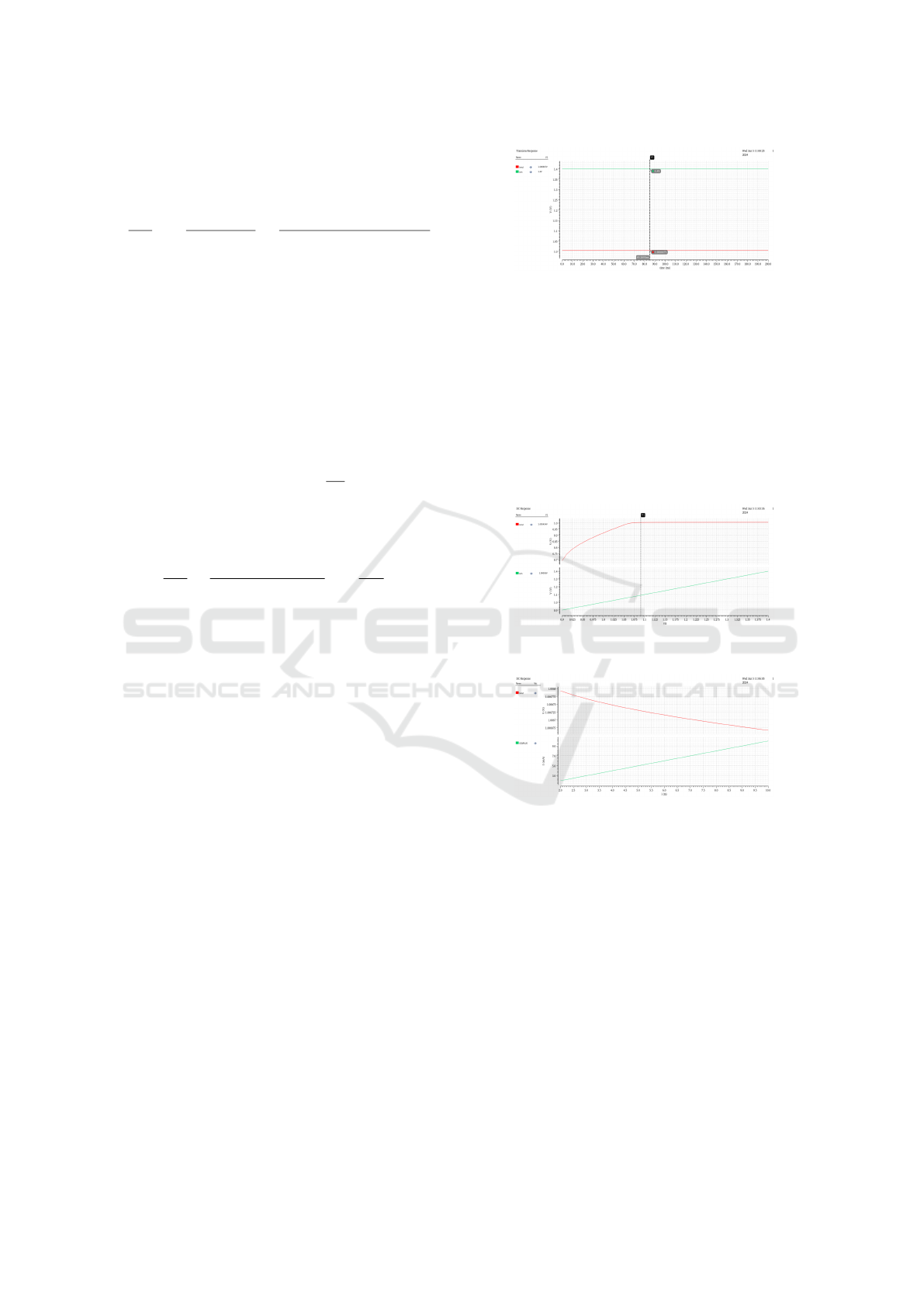
4 RESULTS
4.1 Voltage Regulation
To evaluate the LDO design’s performance, it was put
through a number of tests. Despite variations in input
voltage and load current, the output voltage remained
constant at 1.0066V fig[3], demonstrating the LDO’s
resilience to variable circumstances. In systems like
RF circuits, where a consistent power source is es-
sential for dependable operation, this is particularly
significant.
Figure 3: Input and Output of LDO.
4.2 Line and Load Regulations
With a measured value of 1.07 V/V, which indi-
cates little variance, line regulation guarantees that
the LDO maintains a steady output even when input
voltage changes fig[4]. At 16.33 mV/A, load regu-
lation gauges the LDO’s capacity to maintain output
stability when load current varies fig[5]. This means
that the output voltage varies somewhat in response to
changes in current demands.
Figure 4: Line Regulation.
Figure 5: Load Regulation.
4.3 Power Supply Rejection Ratio
(PSRR)
The LDO’s capacity to efficiently suppress power
supply noise was demonstrated by its high PSRR of
-55.82 dB at 1 MHz fig[6]. This is essential for RF
circuits because it protects sensitive components and
ensures that input noise doesn’t impact the output.
4.4 Transient Response
When tested with abrupt variations in load current, the
LDO’s transient response revealed a minimal voltage
overshoot of 113.84 mV and an undershoot of 113.63
Wide Band High PSRR LDO Voltage Regulator
15
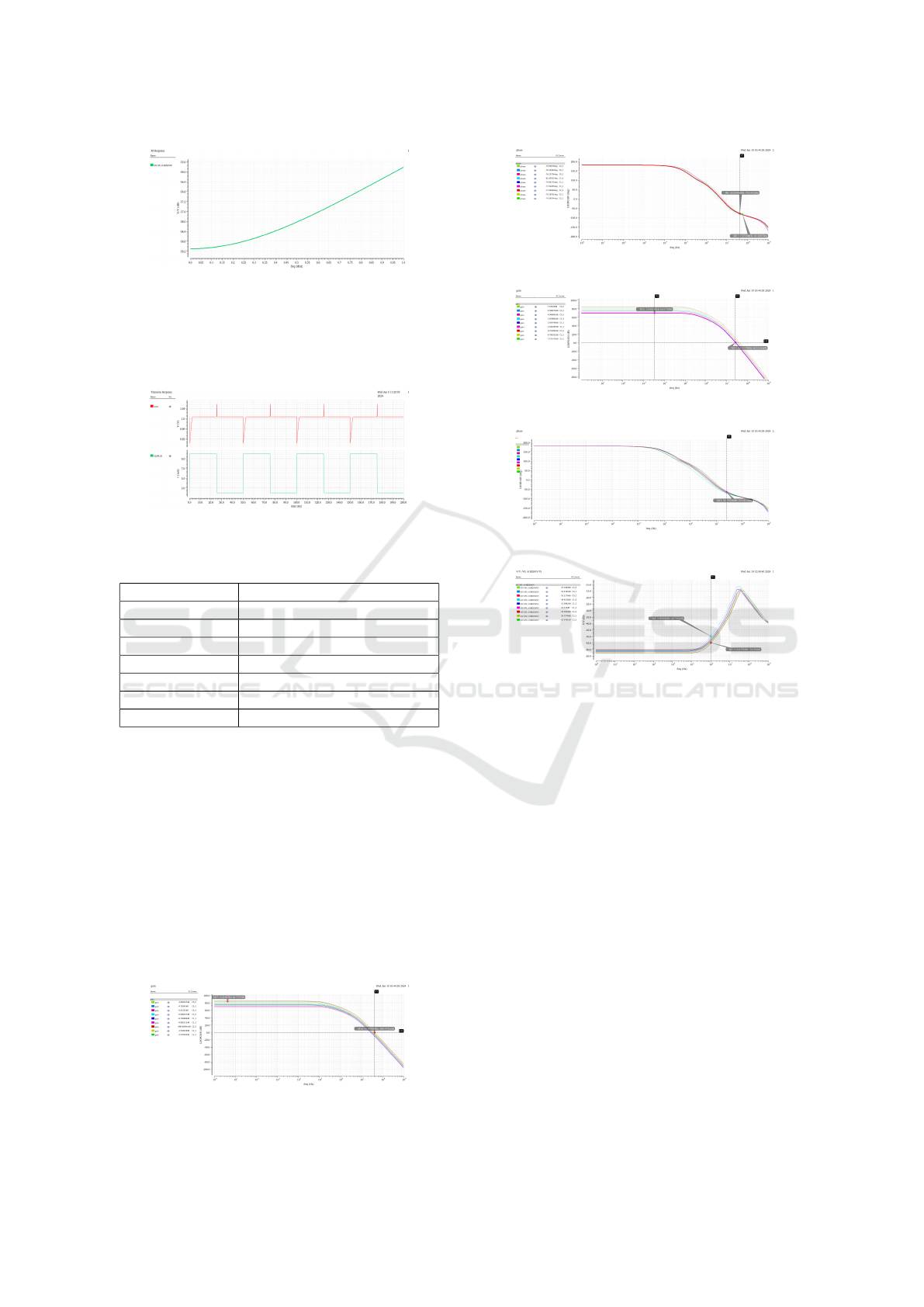
Figure 6: PSRR.
mV fig[7]. It is perfect for systems with abrupt vari-
ations in power demand because of its fast recovery,
which guarantees steady output voltage even in dy-
namic situations.
Figure 7: Transien Response.
Table 1: Performance Parameters
Specifications Wideband High PSRR LDO
Input Voltage 1.4 V
Output Voltage 1.066 V
Line Regulation 1.07 V/V
Load Regulation 16.33 mV/A
Overshoot 113.84 mV
Undershoot 113.63 mV
PSRR -55.82 dB (at 1 MHz)
4.5 PVT Analysis
PVT (process, voltage, temperature) analysis assesses
the effects of temperature changes, voltage swings,
and process variations on LDO performance. Even
in difficult situations, it guarantees a high PSRR and
steady output voltage, enhancing system dependabil-
ity and reducing noise.
Figure 8: Best Case Gain.
Figure 9: Best Case Phase.
Figure 10: Worst Case Gain.
Figure 11: Worst Case Phase.
Figure 12: PVT Anlaysis for PSRR.
4.6 LAYOUT
At 274.29 µm × 40.2 µm (0.011026 mm²) fig[13], the
LDO arrangement is ideal for both power and signal
integrity. Ten rows and one hundred columns of 1000
MOSFETs make up its pass element. Reliability and
compliance for production are ensured by the layout
passing DRC (Design Rule Check) inspections and
LVS (Layout vs. Schematic) verification.
5 CONCLUSION
For steady, noiseless power delivery in delicate ana-
log and radio frequency circuits, the Wideband High
PSRR LDO is essential. It is constructed with a
PMOS pass element and UMC 180nm CMOS tech-
nology, which guarantees low dropout voltage, low
power loss, and good transient responsiveness. It is
perfect for RF circuits due to its high PSRR over a
broad frequency range. Because of its small size, low
quiescent current, and thermal efficiency, the design
is ideal for portable electronics and Internet of Things
INCOFT 2025 - International Conference on Futuristic Technology
16
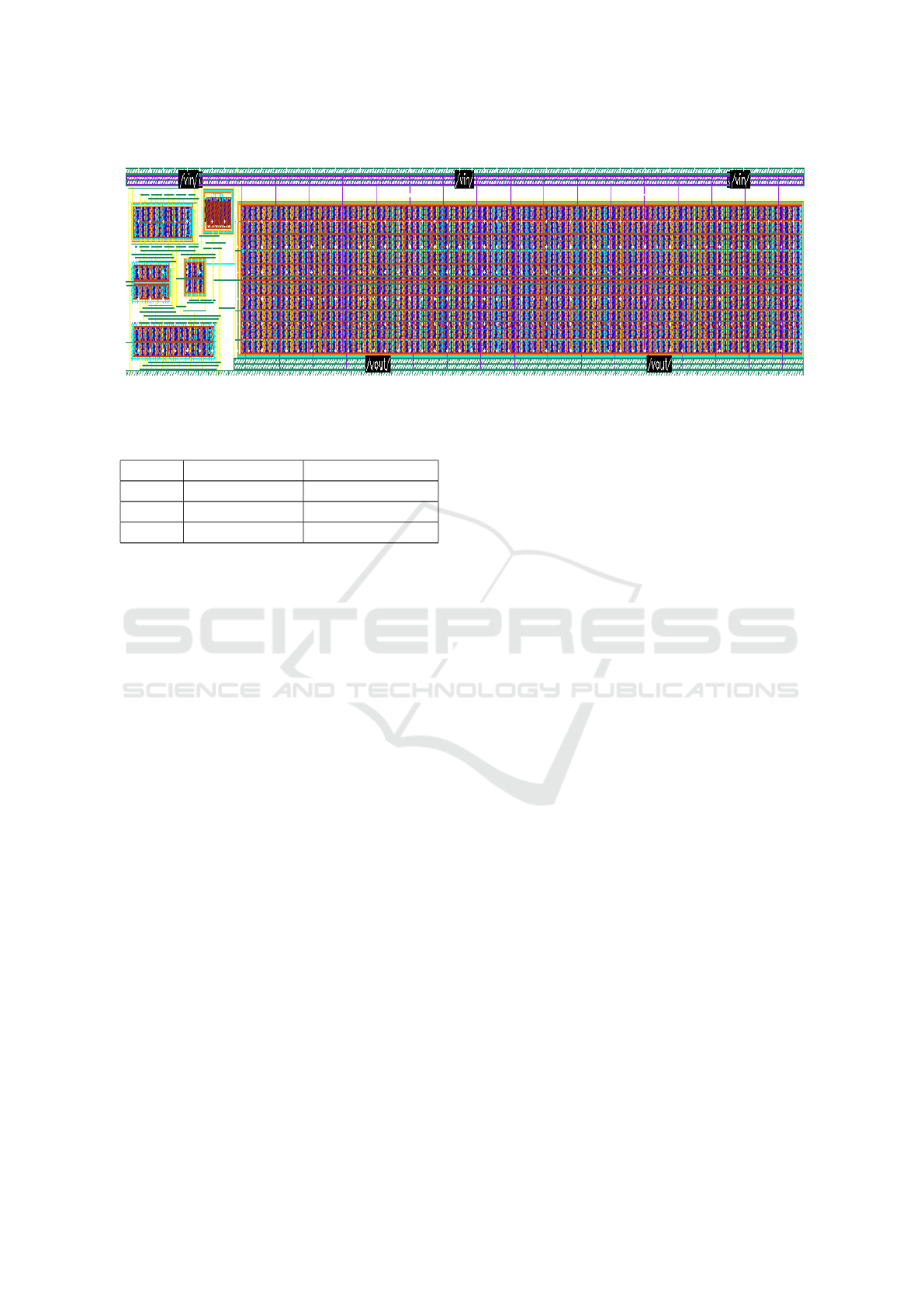
Figure 13: LAYOUT OF LDO
Table 2: PVT Analysis
Best Case (ff) Worst Case (ss)
Gain 84.7737 dB 69.6739 dB
Phase -78.1412deg -65.6131deg
PSRR -54.986dB -49.7356dB
applications. This LDO offers a cost-effective solu-
tion for consumer electronics, automotive, and indus-
trial applications by striking a balance between per-
formance, efficiency, and durability.
6 FUTURE SCOPE
High-efficiency, low-noise power management will
become more and more necessary as electronics get
more complicated. With future developments focus-
ing on critical performance areas, LDOs with high
PSRR will be essential in technologies like 5G, IoT,
and automotive systems.
• Integration with PMICs: LDOs will eventually
be integrated into PMICs, allowing for reduced
prices, improved efficiency, and smaller sizes. In
complicated systems, this will enhance coordi-
nated power supply.
• Improved Noise Performance and Wideband
PSRR: The requirement for greater PSRR at wide
frequencies will be met by adaptive biasing, feed-
forward compensation, and multi-loop feedback,
which will efficiently filter noise in 5G and RF
circuits.
• Efficiency and Low Power Consumption: LDOs
will favor ultralow quiescent current and optimal
dropout voltage due to the advancement of green
technology, which will increase battery-powered
devices’ efficiency.
• Research in New Materials: Future LDOs may be
able to attain lower power loss thanks to wide-
bandgap materials like GaN and SiC, improving
designs for high-frequency, high-power applica-
tions.
6.0.1 Reference Text and Citations
(Li et al., 2019). (Wang et al., 2016). (Tham and
Nagaraj, 1995). (Neri et al., 2015). (Rincon-Mora
and Allen, 1998). (Huang et al., 2016). (El-Nozahi
et al., 2010). (Shen et al., 2006).
REFERENCES
El-Nozahi, M., Amer, A., Torres, J., Entesari, K., and
Sanchez-Sinencio, E. (2010). High psr low drop-
out regulator with feed-forward ripple cancellation
technique. IEEE Journal of Solid-State Circuits,
45(3):565–577.
Huang, M., Lu, Y., Sin, S.-W., U, S.-P., Martins, R. P., and
Ki, W.-H. (2016). Limit cycle oscillation reduction
for digital low dropout regulators. IEEE Transactions
on Circuits and Systems II: Express Briefs, 63(9):903–
907.
Li, Q., Wang, K., and Zhao, J.-j. (2019). A capacitor-less
ldo with fast transient response using push-pull buffer.
In 2019 IEEE International Conference on Electron
Devices and Solid-State Circuits (EDSSC), pages 1–3.
Neri, F., Brauner, T., De Mey, E., and Schippel, C. (2015).
Low-power, wide supply voltage bandgap reference
circuit in 28nm cmos. In 2015 IEEE Jordan Confer-
ence on Applied Electrical Engineering and Comput-
ing Technologies (AEECT), pages 1–6.
Rincon-Mora, G. and Allen, P. (1998). A low-voltage, low
quiescent current, low drop-out regulator. IEEE Jour-
nal of Solid-State Circuits, 33(1):36–44.
Wide Band High PSRR LDO Voltage Regulator
17

Shen, L.-g., Yan, Z.-s., Zhang, X., Zhao, Y.-f., and Lu, T.-
j. (2006). Design of low-voltage low-dropout regu-
lator with wide-band high-psr characteristic. In 2006
8th International Conference on Solid-State and Inte-
grated Circuit Technology Proceedings, pages 1751–
1753.
Tham, K.-M. and Nagaraj, K. (1995). A low supply voltage
high psrr voltage reference in cmos process. IEEE
Journal of Solid-State Circuits, 30(5):586–590.
Wang, L., Mao, W., Wu, C., Chang, A., and Lian, Y. (2016).
A fast transient ldo based on dual loop fvf with high
psrr. In 2016 IEEE Asia Pacific Conference on Cir-
cuits and Systems (APCCAS), pages 99–102.
INCOFT 2025 - International Conference on Futuristic Technology
18
