
Design and Modelling of Materials Based Memristors Designs in
Flexible Electronics from Synapse to Systems and Applications
T. Vasudeva Reddy
1
, K. Madhava Rao
1
, V Sreelatha Reddy
2
, N. Swapna
3
, Arunkumar Madupu
4
,
and M S S Bhargav
1
1
Dept. of ECE. B V Raju Institute of Technology, Narsapur, Medak (dist), Telangana, India
2
EIE Dept., CVR College of Engineering Ibrahimpatnam, Hyderabad, India
3
Department of ECE, Guru Nanak Institutions Technical Campus, Hyderabad, Telangana, India
4
Dept. of ECE, Malla Reddy College of Engineering and Technology, Hyderabad, India
Keywords: Memristor, Neromorphic Computing, Non-Volatile Memory, Artificial Intelligence, Flexible Electronics.
Abstract: Memristors, or memory resistors, have garnered significant attention in recent years due to their potential to
revolutionize computing, memory storage, and analog circuit design. This review article provides a
comprehensive overview of the research progress and developments in Memristor designs, spanning from
fundamental concepts to cutting-edge applications. We discuss the evolution of Memristor architectures, from
initial titanium dioxide- based devices to advanced spintronic, ferroelectric, and phase- change materials-
based designs. Notable advancements in Memristor modelling, simulation, and fabrication techniques are
highlighted, alongside significant breakthroughs in scalability, reliability, and performance. The article
explores various applications of memristors, including on-volatile memory (NVM) technologies the
challenges and future directions for Memristor research, improved device uniformity, and the integration of
memristors with emerging technologies such as grapheme, 2D materials, and quantum computing.
1 INTRODUCTION
The emergence of memristors has transformed the
computing and electronics landscape, offering
unparalleled efficiency, security, and adaptability. By
combining memory and resistance, memristors
enable innovative solutions for non-volatile memory,
neuromorphic computing, and analog- to-digital
conversion. Their exceptional characteristics,
including low power consumption and high switching
speeds, make them ideal for adaptive computing
applications.
Memristor technology has undergone significant
advancements, from initial titanium dioxide-based
designs to cutting-edge spintronic, ferroelectric, and
phase-change materials-based architectures. These
innovations have substantially enhanced
performance, scalability, and reliability. Furthermore,
breakthroughs in modelling, simulation, and
fabrication techniques have accelerated research.
Memristors have extensive applications in various
fields, including non-volatile memory, neuromorphic
computing, and secure computing platforms.
However, challenges persist, such as standardizing
testing protocols, improving device uniformity, and
integrating memristors with emerging technologies.
Ongoing research focuses on addressing these
challenges and exploring new applications, including
Memristor-based neural networks and cognitive
computing architectures. This transformative
technology has the potential to revolutionize
computing, electronics, and artificial intelligence.
Key areas of research include: Memristor design and
materials, Modelling and simulation techniques,
Fabrication and characterization methods,
Computing, memory, and analog circuit applications
By investigating memristors' potential, researchers
can unlock new frontiers in computing and
electronics, driving innovation and advancement.
Figure 1 indicates the overview of memristor with the
materials, structural design, performance and its
applications.
844
Reddy, T. V., Madhava Rao, K., Sreelatha Reddy, V., Swapna, N., Madupu, A. and Bhargav, M. S. S.
Design and Modelling of Materials Based Memristors Designs in Flexible Electronics from Synapse to Systems and Applications.
DOI: 10.5220/0013605900004664
Paper published under CC license (CC BY-NC-ND 4.0)
In Proceedings of the 3rd International Conference on Futuristic Technology (INCOFT 2025) - Volume 2, pages 844-851
ISBN: 978-989-758-763-4
Proceedings Copyright © 2025 by SCITEPRESS – Science and Technology Publications, Lda.
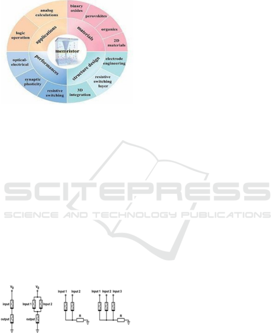
Figure 1: Memristor and overview
2 MATERIALS & MECHANISM
A Review on Non-Volatile and Volatile Emerging
Memory Technologies" by S. Raman Sundara Raman
examines emerging memory solutions, focusing on
memristors. Memristors offer energy efficiency, high
density and fast switching, making them ideal for
next-generation memory. Key findings include
enhanced performance through design optimization,
improved uniformity via material exploration and
fabrication techniques, and the importance of
standardized testing. Challenges persist in
uniformity, scalability and integration.
Recommendations emphasize interdisciplinary
collaboration, targeted funding and standardization,
driving innovations in energy-efficient computing,
quantum computing and neuromorphic computing.
Basic element required for the designs are the
memristors indicated in below Figure 2 Memristor
bases Inverter designs.
Figure 2: Memristor bases Inverter designs
3 RESEARCH WORK
PROPOSED, ADVANTAGES
AND LIMITATIONS
Modern computer systems, based on the Von-
Neumann architecture, face a significant performance
bottleneck dueto the disparity between processing
speed and memory access times, known as the
"memory-wall" problem. Despite advancements in
CPU design, from in-order to out- of-order execution,
memory performance has struggled to keep pace
(Raman, 2024). To address this, researchers have
explored various memory technologies, including
volatile options like Static Random Access Memory
(SRAM), Dynamic RandomAccess Memory
(DRAM), and Embedded DRAM (eDRAM), as well
as non- volatile alternatives such as NAND/NOR
Flash, Resistive Random Access Memory (RRAM),
Magneto-resistive Random Access Memory
(MRAM), and Ferroelectric Field Effect
Transistor(FeFET). SRAMs, in particular, have been
optimized with 6T and 8T structures, with the 8T
design offering improved performance in high-
performance cache designs. Understanding the
tradeoffs between energy, area, and performance in
these technologies is crucial for developing
innovative solutions to overcome the memory-
wallchallenge and enable continued advancements in
computing performance.
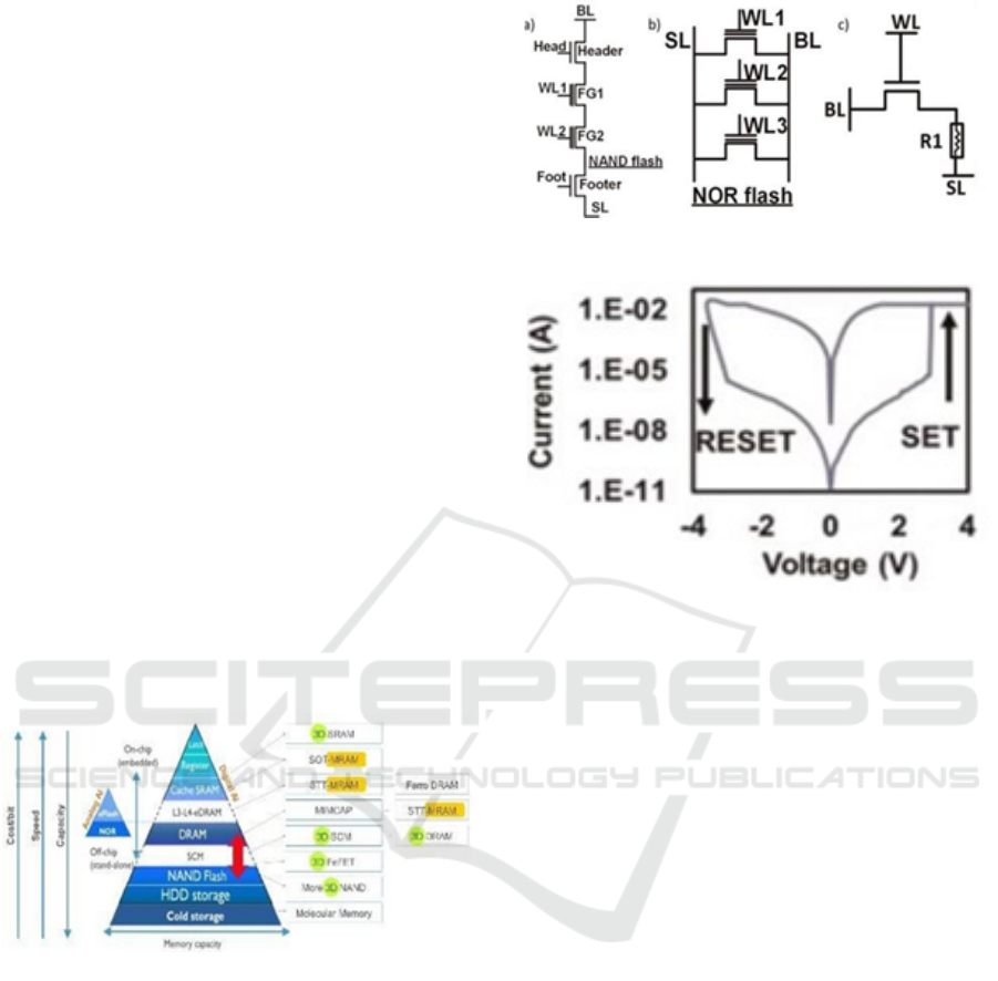
3.1 The 6T SRAM design
Utilizing a shared read-write port, faces significant
limitations, including complex constraints such as
access transistor drive strength, PMOS/NMOS ratio,
and NMOS transistor strength. Additionally, read
operations require bit line precharging and sensing
voltage differences, while retention phases are
plagued by data leakage, bit-flip risks, and increased
power consumption (Ibhanupudi et al., 2023). To
address these challenges, alternative designs like 8T
SRAM have emerged, featuring decoupled read and
write ports, simplified design constraints, reduced
latency, and improved performance. Furthermore,
researchers are exploring emerging non-volatile
memory technologies, including Magneto-resistive
Random Access Memory (MRAM), to overcome the
volatility and design limitations of traditional SRAM,
enabling faster, more efficient, and scalable memory
solutions.
Design and Modelling of Materials Based Memristors Designs in Flexible Electronics from Synapse to Systems and Applications
845
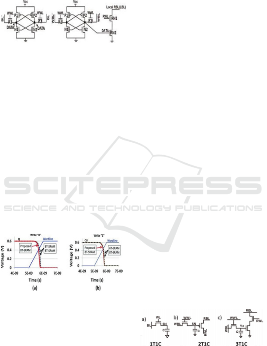
Figure 3a) 6T SRAM 3b) 8T SRAM
Leverages magnetism and spin Hall effects to
store data, utilizing resistance variations to represent
different states. It boasts exceptional endurance of up
to 10^15 cycles, lower write voltage, and reduced
latency compared to Resistive Random Access
Memory (RRAM). MRAM types include Spin
Transfer Torque (STT MRAM) and Spin Orbit
Torque MRAM (SOT MRAM), distinguished by
their writing mechanisms. The MRAM bitcell
consists of a magnetic tunnel junction (MTJ) with
three layers: pinned, spacer, and free, where the
relative orientation determines the device's magneto-
resistance. leverages magnetism and spin Hall effects
to store data, utilizing resistance variations to
represent different states. It boasts exceptional
endurance of up to 10^15 cycles, lower write voltage,
and reduced latency compared to Resistive Random
Access Memory (RRAM). MRAM types include
Spin Transfer Torque (STT MRAM) and Spin Orbit
Torque MRAM (SOT MRAM), distinguished by
their writing mechanisms. The MRAM bitcell
consists of a magnetic tunnel junction (MTJ) with
three layers: pinned, spacer, and free, where the
relative orientation determines the device's magneto-
resistance.
Figure 4a) write 0 4b) write 1 analysis
MRAM stores data by switching between
high/low resistance states based on current direction.
Despite being ready for mass production, MRAM
faces integration and resistance ratio challenges.
However, its advantages make it a promising
technology for next-gen memory solutions in high-
performance computing, data storage, AI, and IoT,
withongoing research focused on enhancing
performance and scalability. From the figure 1b, 8T
SRAM architecture offers improved performance and
reduced design constraints compared to traditional 6T
SRAM (Wicht et al., 2024). The 8T SRAM
architecture surpasses traditional 6T SRAM in
performance and simplicity, featuring decoupled
read/write ports, independent read port transistors,
and full swing discharge of RBL during read
operations, resulting in a 1-cycle reduction in read-
after-write cycle time (from 3 to 2 cycles) and 50%
reduction in discharge latency (Raman, et al. , 2024).
In contrast, 6T SRAM is hindered by volatility,
intricate design constraints, limited scalability (less
than 10nm), high power consumption (up to 50% of
total power), and bandwidth restrictions (limited to
100MHz) (Ibhanupudi, Raman, et al. , 2023). To
overcome these limitations, researchers are exploring
novel memory technologies and architectures,
including emerging options like MRAM, which
promises 2- 5x faster performance, 3-5x lower power
consumption, and 10-20x improved scalability
(Wicht, Nirschl, et al., 2023), (Raman, Nibhanupudi,
et al., 2022). Further innovations in design, materials,
and technology are crucial for next- generation
computing solutions.
Commodity DRAMs, utilizing the 1T1C
structure, offer high storage density but are volatile,
requiring periodic refreshes (Morita, et al. , 2007),
(Verma, Chandrakasan, et al. , 2007)
. The write operation involves charging the bit cell
capacitor (Chang, et al. , 2008), (Farmahini, Farahani,
et al. , 2015), (Nibhanupudi, Raman, et al. , 2021),
while the read operation requires precharging the bit
line to Vcc/2 and sensing voltage drops.However, this
design is susceptible to process variations and
discharge issues. Alternative structures like 2T1C and
3T1C DRAMs have been proposed (Ishiuchi, et al. ,
1997), featuring decoupled read and write ports and
non-disruptive read mechanisms9110. Despite
advancements, DRAMs face issues with long access
latencies, reduced metal layers, and limited
bandwidth. Embedded DRAMs (eDRAMs) address
these concerns through monolithic integration with
logic transistors, enabling stacking and increased
bandwidth (Koob, et al. , 2010), (Ali, Jaiswal, et al. ,
2019), (Raman, Xie, et al. , 2021).
Figure 5a) 1T1C b) 2TIC c)3T1C
INCOFT 2025 - International Conference on Futuristic Technology
846
Traditional DRAM designs face significant
hurdles, Including volatility, manufacturing
variability, and latency issues. Novel architectures,
such as 2T1C and 3T1C DRAMs, offer enhanced
performance through separate read and write
pathways. Embedded DRAMs (eDRAMs) integrated
with logic transistors boost bandwidth. However,
researchers must still tackle key challenges:
mitigating volatility, reducing latency, and
innovating DRAM structures. Next-generation
memory technologies hinge on resolving these issues.
Future solutions must harmonize performance, power
efficiency, and scalability to meet escalating data
storage needs and drive technological advancements.
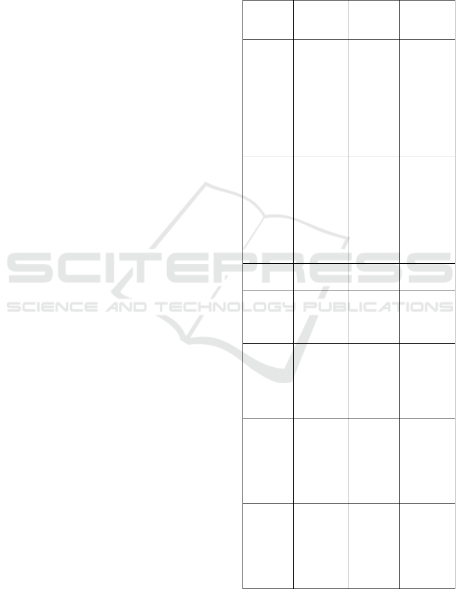
3.2 Non-Volatile Memory Technologies
Like NAND/NOR flash, enable data storage without
power. Used in SSDs, they outperform magnetic
memories but lag behind SRAM/DRAM. Emerging
solutions, including RRAM and MRAM, address
performance gaps, promising faster, scalable, and
energy-efficient storage for next- generation
computing, storing '0' (Wong, et al. , 2012). Erasing
releases trapped electrons by driving the control gate
with a negative or 0 voltage. NAND flash has higher
density, high write performance, and low read
performance compared to NORflash.
Figure 6: Pyramid stricture of Non-volatile technologies
NAND flash memory technology utilizes
floating-gate transistors to store data, with a control
gate trapping electrons. The write operation involves
programming (writing '0') and erasing (writing '1') by
modulating the threshold voltage (Bez, et al. , 2003).
Programming requires a high voltage, attracting
electrons onto the floating gate, increasing the
threshold voltage and storing '0' (Wong, et al. , 2012).
Erasing releases trapped electrons by driving the
control gate with a negative or 0 voltage. NAND flash
has higher density, high write performance, and low
read performance compared to NORflash.
Figure 7.a) NAND b) NOR flash, c) RRAM bitcell
Figure 7.d) RRAM I-V characteristics
NAND flash's write operation involves driving
the bitlineto '0', word line to 20V, and header device
to 4V. Erase operations initialize the bit line to 0, float
source and drain voltages, and keep word lines at 0.
Read operations drive the bit line high, source line
low, and word line low for the selected row (Raman,
Xie, et al. , 2021), (Compagnoni, , et al. , 2017),
(Boppidi, Raman, et al. , 2012). NAND flash
advantages include storing multiple levels in a single
bit- cell and suitability for SSDs. However, it suffers
from high operation voltages, thermal bottleneck
issues (Micheloni, Crippa, et al. , 2010), (Goda,
2021)., and limited scalability (Bez, et al. ,
2003).Future prospects include stacking multiple
layers with minimal coupling coefficient to improve
density and performance. Researchers continue to
explore innovations in NAND flash technology to
address its limitations and enhance its capabilities
(Bez, et al. , 2003), (Wong, et al. , 2012), (Shen, et al.
, 2020).
3.3 Magneto-Resistive Random Access
Memory (MRAM)
Magneto resistive Random Access Memory
(MRAM)leverages magnetism and spin Hall effects
to store data, utilizing resistance variations to
represent different states. It boasts exceptional
Design and Modelling of Materials Based Memristors Designs in Flexible Electronics from Synapse to Systems and Applications
847

endurance of up to 10^15 cycles, lower write voltage,
and reduced latency compared to Resistive Random
Access Memory (RRAM) (Ielmini, 2021), (Tehrani,
, et al. , 1999). MRAM types include Spin Transfer
Torque (STT MRAM) (Huai, 2008), (Fong, et al. ,
2016) and Spin Orbit Torque MRAM (SOT
MRAM), distinguished by their writing mechanisms.
The MRAM bitcell consists of a magnetic tunnel
junction (MTJ) with three layers: pinned, spacer, and
free, where the relative orientation determines the
device's magneto-resistance.
Figure 8: (i)STT-MRAM and (ii) FeFET bitcell
3.4 RRAM I-V Characteristics
NAND flash's write operation involves driving the
bitlineto '0', wordline to 20V, and header device to
4V. Erase operations initialize the bitline to 0, float
source and drain voltages, and keep wordlines at 0.
Read operations drive the bitline high, source line
low, and wordline low for the selected row. NAND
flash advantages include storingmultiple levels in a
single bit- cell and suitability for SSDs. However, it
suffers from high operation voltages, thermal
bottleneck issues., and limited scalability
Futureprospects include stacking multiple layers with
minimal coupling coefficient to improve density and
performance. Researchers continue to explore
innovations in NAND flash technology to address its
limitations and enhance its capabilities.
The device's switching is current-direction
dependent, with current flowing from the pinned to
free layer switching the free layer from parallel to
antiparallel (low to high resistance), representing a '0'.
Conversely, current flowing from free to pinned layer
switches from antiparallel to parallel (high to low
resistance), representing a '1'. Read operations
involve applying voltage to the bitline and souceline,
with the current through the MTJ indicating the
device's magneto-resistance. While STT MRAMs are
now ready for mass production, overcoming
fabrication complexities, MRAM still faces
challenges such as integration complexity and lower
OFF-to-ON resistance ratio.
Despite these challenges, MRAM's advantages
make it a promising technology for next-generation
memory solutions, with ongoing research focused on
enhancing its performance and scalability. Its
potential applications include high- performance
computing, data storage, and emerging technologies
like artificial intelligence and Internet of Things
(IoT). As MRAM technology continues to evolve, it
is likely to play a significant role in shaping the future
of memory and computing.
4 FERROELECTRIC FIELD
EFFECT TRANSISTOR (FEFET)
Ferroelectric Field-Effect Transistors (FeFETs)
(Dünkel et al. 2017) are a promising non-volatile
memory technology, offering exceptional density,
speed, and compatibility with established CMOS
nodes. By leveraging ferroelectric capacitors,
FeFETs store data in a manner similar to DRAM.
However, initial designs faced significant challenges,
including high program/erase voltage requirements
and reduced retention times due to inherent
depolarizing fields. To overcome these limitations,
researchers have developed innovative designs, such
as recessed FeFETs and Ferroelectric Memory Field-
Effect Transistors (FeMFETs) (Yurchuk, et al. ,
2016). These advancements enable optimized
ferroelectric capacitor integration, reduced write
voltage, and enhanced performance. Nonetheless,
FeMFETs introduce a floating node vulnerable to
noise and process variations, impacting retention
time and read voltage. FeFETs' write operations
involve applying a gate voltage, with the ferroelectric
capacitor's voltage indicating the stored data. Read
operations utilize a read disturb voltage, creating a
voltage division that increases current through the
MOSFET for a logical '1' and reduces it for a '0'.
While FeFETs hold great promise, addressing
voltage and retention challenges remains crucial for
their widespread adoption. (Raman, Nibhanupudi, et
al. , 2021)
5 COMPARITIVE ANALYSIS
Non-Volatile Memory (NVM) technologies have
revolutionized data storage, offering high
performance, low power consumption, and durability.
Several prominent NVM technologies exist, each
with unique advantages and disadvantages. Flash
Memory: Flash memory is widely adopted due to its
high density and low cost. However, it has limited
write endurance and slow write speeds, making it less
INCOFT 2025 - International Conference on Futuristic Technology
848
suitable for applications requiring frequent data
updates. Despite these limitations, flash memory
remains popular in consumer electronics, mobile
devices, and solid-state drives (SSDs). Spin-Transfer
(Fong et al. 2016; Dünkel et al. 2017) Torque
Magnetic Recording (STT- MRAM). STT-MRAM
boasts high speed, low power consumption, and
infinite write endurance, making it ideal for mobile
devices, data centers, and cache memory
applications. However, its high cost and limited
density hinder widespread adoption.
5.1 Resistive Random-Access Memory
(RRAM)
RRAM offers low power consumption, high speed,
and scalability, but its limited write endurance and
variability pose challenges. RRAM is suitable for
mobile devices, IoT devices, and xeromorphic
computing applications.
5.2 Phase Change Memory (PCM)
PCM combines high density, fast write speed, and
low power consumption, but its limited write
endurance and highcost restrict its use to data centers,
cloud storage, and AI applications.
5.3 Memristor-Based Memory
Memristor-based memory excels in low power
consumption, high speed, and infinite write
endurance. However, its limited density and high
cost currently limit its adoption. Potential
applications include neuromorphic computing, AI,
and IoT devices.
5.4 Comparison and Future Directions
A comparison of these technologies reveals trade-
offs between density, speed, power, endurance, and
cost. Future research should focus on scaling NVM
technologies to smaller nodes, improving write
endurance and speed, reducing power consumption,
developing hybrid memory solutions, and exploring
emerging materials and architectures. Each NVM
technology has strengths and weaknesses.
Understanding these trade-offs is crucial for
selecting the optimal solution for specific
applications. Flash memory excels in density and
cost, while STT-MRAM offers high speed and
endurance. RRAM balances speed, power, and
density, while PCM boasts high density and speed.
Meritor-based memory promises infinite endurance
but lags in density.
Table 1: Comparative analysis of Functional models
Feature RRAM PCM
Memristor-
based
Memory
Technolo
gy
Relies on
resistive
switching
in metal
oxide
layers.
Uses the
phase
change
between
amorphou
s and
crystalline
states in
chalcogen
ide
materials.
Exploits
the intrinsic
property of
memristors
to
remember
resistance
based on
previous
states.
Switching
Mechanis
m
Ionic
movement
in the
dielectric
layer to
form/ruptur
e
conductive
filaments.
Thermal-
induced
phase
transition
in
materials
like
Ge2_22
Sb2_22
Te5_55.
Change in
resistance
due to ion
migration
or electron
tunneling
within the
memristor
material.
Non-
volatility
Yes Yes Yes
Write
Speed
Very fast
(nanosecon
ds to
microsecon
ds).
Moderate
(microsec
onds).
Extremely
fast (sub-
nanosecond
s possible).
Enduranc
e
Moderate
to high
(106^66-
108^88
cycles).
Moderate
(106^66-
107^77
cycles).
High
(potentially
>1012^121
2 cycles,
depending
on
material
)
.
Density
High
(scaling
possible to
sub-10
nm).
Moderate
(limited
by
thermal
cross-talk
and
scalability
).
Very high
(scales to
atomic
dimensions
).
Energy
Consumpt
ion
Low power
for
read/write
operations.
High
power
required
for
thermal
operations
.
Very low
due to
energy-
efficient
resistance
change
mechanism
.
Design and Modelling of Materials Based Memristors Designs in Flexible Electronics from Synapse to Systems and Applications
849

Retention
Excellent
(up to 10
years or
more).
Good (10
years or
more).
Excellent
(theoretical
ly infinite
retention
due to
physical
resistance
state
)
.
Fabricatio
n
Compatible
with
CMOS
processes;
simpler
than PCM
but requires
precise
material
engineering
.
Complex
due to the
need for
thermal
insulation
and
chalcogen
ide
deposition
.
Requires
new
material
sets but
highly
integrable
with
CMOS.
Applicatio
ns
Data
storage,
neuromorp
hic
computing,
IoT
devices.
Enterprise
storage,
archival
memory,
embedded
systems.
Neuromorp
hic
systems,
reconfigura
ble logic,
and future
memory
technologie
s.
Maturity
Commercia
lized but
still in
developme
nt for larger
scale
adoption.
Mature
and
commerci
ally
deployed
in
products
like Intel
O
p
tane.
Emerging,
with
significant
research
focus but
limited
large-scale
deployment
.
Advantag
es
Simple
structure,
fast
switching,
high
density.
High
endurance
, good
retention,
and
multilevel
storage
capability.
Ultra-low
power, high
endurance,
and
compatibili
ty with
future
computatio
nal
p
aradi
g
ms.
Challenge
s
Variability
in
switching,
endurance
issues, and
scalability.
Thermal
cross-talk,
material
degradatio
n, and
power
consumpti
on.
Lack of
standardiza
tion, high
variability,
and
fabrication
challenges
at a large
scale.
6 CONCLUSION & FUTURE
SCOPE
The choice of NVM technology depends on the
specific application requirements. As research
advances, next- generation NVM technologies will
continue to shapethe data storage landscape, enabling
faster, smaller, and more efficient devices.
Memristors are innovative devices that retain their
resistance based on the voltage applied. Since their
conceptualization in 1971 and practical development
in 2008, memristors have garnered significant interest
for their potential to transform the electronics
industry. Memristors have numerous applications,
particularly in non-volatile memory technologies.
Their benefits include high storage density, low
power consumption, and rapid switching speeds.
They are ideal for next-generation memory solutions,
artificial neural networks, deep learning,
reconfigurable RF circuits, microwave devices,
sensors, and Internet of Things (IoT) devices. Despite
their potential, memristors face challenges that must
be addressed. These include enhancing device
uniformityand scalability, integrating memristors
with emerging technologies like graphene and
quantum computing, and improving performance
while reducing power consumption. Researchers are
exploring the integration of memristors with cutting-
edge technologies. Graphene-based memristors offer
enhanced switching speeds and uniformity, while 2D
material-based memristors provide high on/off ratios
and low power consumption. Quantum memristors
enable advanced quantum computing applications.
Memristors are poised to revolutionize the electronics
industry, particularly in non-volatile memory
technologies. Addressing existing challenges and
leveraging emerging technologies will unlock their
full potential. As research advances, memristors will
play a crucial role in transforming the electronics and
computing industries. The future of memristor
technology holds much promise. With ongoing
innovations and breakthroughs, memristors will
continue to shape the landscape of modern
electronics, enabling faster, smaller, and more
efficient devices. Their impact will be felt across
various sectors,from consumer electronics to space
exploration.
REFERENCES
S. Raman Sundara Raman, 2024 “A Review on Non-
Volatile and Volatile Emerging Memory
INCOFT 2025 - International Conference on Futuristic Technology
850

Technologies”, Computer Memory and Data Storage.
IntechOpen
Ibhanupudi SST, Raman SRS, Kulkarni JP. 2023“Phase
transition material assisted low-power SRAM design,
IEEE Transactions on Electron Devices”.
Wicht B, Nirschl T, SchmittLandsiedel D, 2024 “Yield and
speed optimization of a latch-type voltage sense
amplifier. IEEE Journal of Solid-State Circuits“.
Sundara Raman SR, Nibhanupudi SST, Kulkarni JP. 2022
“Enabling In-memory computations in non-volatile
SRAM designs, in IEEE Journal on Emerging and
Selected Topics in Circuits and Systems“.
Morita Y et al. An area-conscious 2007 “low voltage-
oriented 8T-SRAM design under DVS environment”,.
IEEE Symposium on VLSI Circuits. IEEE;
Verma N, Chandrakasan AP. 2007, “A 65nm 8T sub-Vt
SRAM employing sense-amplifier redundancy”, IEEE
Chang L et al. 2008 “An 8T-SRAM for variability tolerance
and low-voltage operation in high-performance
caches”,IEEE Journal of Solid-State Circuits.
Farmahini- Farahani A et al. 2015 “NDA:Near-DRAM
acceleration architecture leveraging commodity
DRAM devices and standard memory modules” IEEE;
Nibhanupudi SST, Sundara Raman, SR, Cassé M, Hutin L,
Kulkarni JP. 2021 “Ultralow-voltage UTBB-SOI-
based, pseudostatic storage circuits for cryogenic,
CMOS application”IEEE Journal on, Exploratory
Solid-State Computational, Devices and Circuits.
Ishiuchi H et al. Embedded DRAM technologies. 1997, “A
Review on Non- Volatile and Volatile Emerging
Memory Technologies s”,IEEE
Belmonte A et al. 2020 “Capacitor-less, long-retention
DRAM cell paving the way towards low- power and
high-density monolithic 3D DRAM, .
IEEEInternational Electron, Devices Meeting (IEDM).
Koob JC et al. 2010 “Design and characterization of a
multilevel DRAM.IEEE Transactions on Very Large
Scale Integration (VLSI) Systems.
Ali MF, Jaiswal A, Roy K.2019, “In-memory low-cost bit-
serial addition using commodity DRAM technology”,.
IEEE Transactions on Circuits and Systems.
Raman SRS, Xie S, Kulkarni JP. 2021 “Compute-in-
eDRAM with backend integrated indium gallium zinc
oxide transistors.” IEEE International,Symposium on
Circuits and Systems,(ISCAS).
Sundara Raman SR, Xie S, Kulkarni, JP. IGZO CIM: 2021
“Enabling In-memory, computations using multilevel
Capacitor less indium–gallium–zinc–oxide- based
embedded DRAM technology ”,, in IEEE Journal on
Exploratory Solid-State Computational Devices and
Circuits.
Compagnoni CM et al. 2017 “Reviewing, the evolution of
the NAND flash technology”,Proceedings of the IEEE.
Boppidi PKR, Raman SS, et al. 2012 “Pt/Cu: ZnO/Nb:
STO memristive dual port for cache memory
applications”. In: AIP, Conference Proceedings
Micheloni R, Crippa L, Marelli A. 2010 “ Inside NAND
Flash Memories”,. Springer. Science Business Media;
Goda A. 2021 ”Recent progress on 3D, NAND flash
technologies”. Electronics.
Bez R et al. 2003 Introduction to flash memory”. IEEE
Wong H-SP et al. 2012 “Metal–oxide RRAM. IEEE
Shen Z et al. 2020 “Advances of RRAM devices”, Resistive
switching mechanisms, materials and bionic synaptic
application.
Ielmini D. 2021 “Modelling the universal set/reset
characteristics of bipolar RRAM by field-and
temperature-driven filament growth” IEEE
Transactions on Electron Devices.
Tehrani S et al. 1999 “Progress and outlook for MRAM
technology”. IEEE Transactions on Magnetics.
Huai Y. 2008” Spin-transfer torque MRAM (STT-
MRAM)”
Fong X et al. KNACK: 2011 “A hybrid spincharge mixed-
mode simulator for evaluating different genres of
spintransfer torque MRAM bit-cells ” IEEE.
Fong X et al. 2016 “Spin-transfer torque memories:
Devices, circuits, and systems”. IEEE.
Dünkel S et al. 2017 “A FeFET based superlow- power
ultra-fast embedded NVM technology for 22nm FDSOI
and beyond” IEEE
Yurchuk E et al. 2016 “Charge-trapping phenomena in
HfO2- based FeFET-type nonvolatile memories”. IEEE
Transactions on Electron Devices.
Raman SRS, Nibhanupudi SST,Saha AK, Gupta S,
Kulkarni JP.2021 “Threshold selector and capacitive
coupled assist techniques for write voltage reduction in
metal– ferroelectric–metal field-effect transistor”.
IEEE Transactions on Electron Devices.
Design and Modelling of Materials Based Memristors Designs in Flexible Electronics from Synapse to Systems and Applications
851
