
Design and Layout of DC-DC Buck Converter
Shreya Anvekar
a
, Sujata Kotabagi
b
, Goutam Giriraddi
c
, Anusha A D
d
and Bhargav Hegde
e
KLE Technological University, Hubballi, India
Keywords:
DC-DC Converter, Buck, Voltage, Voltage Regulator, Step-Down Converter, Layout.
Abstract:
Integrated power management circuits play a pivotal role in portable electronic applications, where high ef-
ficiency, compact form factors, and robust transient response are critical requirements. These circuits, often
realized as DC-DC converters, are indispensable in managing power distribution effectively within a system
while minimizing energy losses. The focus is placed on achieving precise voltage regulation and minimizing
ripple content to ensure stable operation under varying load conditions. This paper details the design, simu-
lation, and implementation of a voltage control mode DC-DC buck converter, specifically tailored to achieve
high efficiency and reliable operation. The proposed design is demonstrated through the development of a
4 MHz prototype fabricated using 180 nm CMOS technology. The prototype effectively regulates an output
voltage while sourcing a maximum load current of 100 mA from a 1.8 V input supply, catering to the de-
mands of low-power portable applications.The circuit architecture incorporates critical components, including
an error amplifier, comparator, and compensator, to establish a robust feedback stabilization mechanism. A
Type-II compensator is employed to enhance the system’s phase margin and ensure stable operation across a
wide range of operating conditions. The design process is supported by extensive simulation-based validation
to optimize the system’s dynamic response and steadystate performance. Experimental measurements, con-
ducted with external filter components (inductor L=6.8H, capacitor C=10 H, reveal favourable performance
characteristics. The results highlight the converter’s ability to maintain a well-regulated output voltage while
exhibiting minimal ripple and rapid transient response to load changes.
1 INTRODUCTION
Voltage regulators are essential components used to
ensure a constant voltage supply to connected cir-
cuits, providing stable operation and protecting sensi-
tive electronics from voltage fluctuations. These reg-
ulators are broadly classified into two categories: lin-
ear and switching regulators. Among switching regu-
lators, the buck converter, also known as a step-down
converter, plays a crucial role in efficiently reducing
DC voltage levels from a higher input to a lower out-
put. A buck converter operates by rapidly switching
on and off using semiconductor devices such as MOS-
FETs, transistors, or IGBTs. This switching action is
controlled by a pulse-width modulation (PWM) sig-
nal, which adjusts the duty cycle to regulate the out-
a
https://orcid.org/0009-0002-5652-5861
b
https://orcid.org/0000-0002-5264-6204
c
https://orcid.org/0009-0006-1444-8959
d
https://orcid.org/0009-0008-2032-9002
e
https://orcid.org/0009-0007-7129-421X
put voltage. Unlike linear regulators, which dissipate
excess energy as heat, buck converters achieve high
power efficiencies, often exceeding 90%, by trans-
ferring energy between the input and output using
inductors, capacitors, and switches. This efficiency
makes buck converters ideal for applications requir-
ing significant power savings and minimal heat gen-
eration. For instance, they are commonly used to step
down higher voltages, such as 12V, to lower levels
like 5V, 3.3V, or 1.8V. These lower voltages are cru-
cial for powering modern electronic devices, includ-
ing USB ports, CPUs, DRAM modules, and various
integrated circuits. The versatility and high efficiency
of buck converters have driven their widespread adop-
tion across numerous industries. With the prolifer-
ation of portable electronic devices, aerospace sys-
tems, and automotive technologies, the demand for
efficient DC-DC converters has surged. Portable de-
vices like smartphones, tablets, and laptops rely on
these converters to maximize battery life while main-
taining performance. Similarly, aerospace systems
use buck converters to power critical subsystems, en-
762
Anvekar, S., Kotabagi, S., Giriraddi, G., A D, A. and Hegde, B.
Design and Layout of DC-DC Buck Converter.
DOI: 10.5220/0013601900004664
Paper published under CC license (CC BY-NC-ND 4.0)
In Proceedings of the 3rd International Conference on Futuristic Technology (INCOFT 2025) - Volume 2, pages 762-768
ISBN: 978-989-758-763-4
Proceedings Copyright © 2025 by SCITEPRESS – Science and Technology Publications, Lda.

suring reliability in extreme environments. In auto-
motive applications, they are integral to electric and
hybrid vehicles, where they manage power distribu-
tion for infotainment systems, sensors, and electric
motor controllers. Unlike AC systems that adjust volt-
age levels using transformers, DC systems depend
on converters like buck regulators for voltage adjust-
ment. This distinction underscores the importance of
buck converters in modern electronic systems, partic-
ularly as DC power sources become more prevalent
in renewable energy systems, data centers, and trans-
portation infrastructure. Buck converters offer sev-
eral advantages that make them indispensable in mod-
ern electronics, including high efficiency, compact de-
sign, the ability to operate with a wide input volt-
age range, and reliable performance across diverse
environmental conditions. Their ability to step down
DC voltages with high efficiency and low energy loss
makes them essential for powering a wide range of de-
vices, from consumer electronics to critical aerospace
and automotive systems. As technology advances and
the demand for portable and sustainable power solu-
tions grows, the role of buck converters will continue
to expand, ensuring stable and efficient power deliv-
ery across an ever-widening array of applications.
2 LITERATURE SURVEY
The paper (Sudharshan et al., 2018) ”Design and Sim-
ulation of DC-DC Buck Converter using Cadence
Tool” details the development of a buck converter de-
signed to step down a variable input voltage between
3V and 8V to a stable 1.2V output, using a switch-
ing frequency of 1MHz. The design employs PMOS-
FET and NMOSFET switches in the power stage, an
error amplifier with an 84dB gain and 20MHz unity-
gain bandwidth, and a comparator for PWM signal
generation. Implemented with Cadence software and
180nm technology, the simulations confirmed effec-
tive voltage regulation, which was validated through a
hardware prototype that demonstrated consistent per-
formance with the simulated results. This approach
is particularly suited for low-power applications such
as mobile devices and LED lighting. Article (An-
vekar et al., 2024) develops a folded cascode CMOS
op-amp in 0.18µm technology, DC gain of 55dB, a
phase margin of 66.87 degrees, and the amplifier’s
bandwidth is reported at 222kHz (-3dB) for a 1pF
load. The paper (Zhang et al., 2015) proposed design
of a two-level recursive gain-boosted amplifier is de-
vised to augment the gain while preserving the over-
all bandwidth. The design intricately considers the
interplay among the core amplifier’s gain bandwidth
product (GBP), regulation amplifiers, and nested gain
boosters. Remarkably, the design attains an excep-
tionally high DC gain of 94.8 dB alongside a phase
margin of 56 degrees.
The paper(Tabbat et al., 2020) presents a study
and analysis of a DC-DC soft switched buck con-
verter, focusing on enhancing efficiency and reducing
losses in power conversion. The proposed converter
incorporates an auxiliary inductor and two capaci-
tors to achieve zero-voltage switching during turn-on
and near soft switching during turn-off, eliminating
switching and reverse recovery losses. The research
highlights the converter’s experimental and theoreti-
cal efficiencies, demonstrating a 96.experimental ef-
ficiency at 200 W output power and a 96.78% theo-
retical efficiency, surpassing other structures in terms
of efficiency and simplicity.The paper (Soheli et al.,
2018) references the work of R. L. Steigerwald on
high-frequency resonant transistor DC-DC convert-
ers, emphasizing the importance of efficient power
conversion in industrial electronics. It also cites J.
Tucker’s technical brief on using a buck converter in
an inverting buckboost topology, highlighting the rel-
evance of various converter configurations for specific
applications. Additionally, the paper mentions M. Iu-
lian’s research on a topology for a positive buck-boost
switching regulator, showcasing the continuous ad-
vancements and ongoing research in the field of DC-
DC converters. The paper (Gupta and Phulambrikar,
2014) presents a generalized model of a buck con-
verter aimed at reducing the size, space, and weight
of converter/inverter circuits through the use of high
switching frequency devices. A decision matrix was
employed to select the optimal buck converter topol-
ogy, taking into account factors such as linearity, volt-
age transfer ratio, and ease of component implemen-
tation. The operation of the buck converter is de-
scribed by equations for different states, including
when the switch is on, off, or both the switch and
diode are off. The study underscores the importance
of a control circuit for the buck converter, identifying
the microprocessor as the optimal choice for control
circuit implementation.
The paper (Masri et al., 2012) extensively delves
into operational amplifiers (opamps) and their prac-
tical applications, with a specific focus on compar-
ing the performance of folded cascode and telescopic
cascode configurations. It scrutinizes these topolo-
gies in both single-staged and two-staged setups, elu-
cidating their respective advantages and drawbacks.
Notably, it highlights a distinctive feature of folded
cascode op-amps: their capability to manage input
common-mode levels near the supply voltage. Folded
cascode op-amps offer high gain and a wide output
Design and Layout of DC-DC Buck Converter
763

swing, functioning as single-pole op-amps, thus en-
suring stability and a substantial phase margin. The
paper concludes by presenting a performance ma-
trix that compares various op-amp topologies.The pa-
per(Baharudin et al., 2018) examines a DC-DC buck
converter designed for renewable energy applications,
focusing on efficient DC voltage conversion. It em-
phasizes the critical role of adjusting the duty cycle
to match the output voltage with load requirements.
To tackle challenges such as voltage drops across
diodes and harmonic issues, the paper proposes us-
ing a second MOSFET to enhance efficiency. The
study highlights the importance of hardware imple-
mentation and testing, which includes measuring out-
put waveforms, voltage readings, and current flow for
thorough validation and analysis.
The paper (Soheli et al., 2021) introduces a highly
efficient DC-DC buck converter designed for sus-
tainable electronic applications, aiming to surpass
the efficiency of conventional converters. It details
the two operational modes, Continuous Conduction
Mode (CCM) and Discontinuous Conduction Mode
(DCM), emphasizing the use of ideal components for
accurate values and improved power efficiency. The
proposed converter’s performance is compared to tra-
ditional converters based on switching frequency and
load variations, demonstrating superior efficiency and
stability. The paper references various works on DC-
DC converter designs, power electronics integration,
and control strategies for switching power converters.
The paper (Kumar et al., ) objective is to develop and
validate a Low Voltage Folded Cascode CMOS Op-
erational Amplifier employing gpdk 0.18µM CMOS
technology. An NMOS differential pair is selected
to minimize power consumption and uphold a high
Unity Gain Frequency (UGF). The design accom-
plishes a gain of 68.6dB, a Phase Margin of 500, and
a UGF of 13.1MHz, while consuming merely 30µW
of power. Additionally, it integrates a sub-threshold
start-up circuit with dynamic body biasing tailored for
boost converters in thermoelectric energy harvesting.
3 OBJECTIVES
Develop a DC-DC buck converter with an input volt-
age of 1.8V and an output voltage of 0.8V, capable
of delivering a load current of 100mA. The design
should operate at a switching frequency of 4MHz and
prioritize maximum power efficiency. Implement the
design using 180nm CMOS technology in the Ca-
dence tool, including its complete layout.
3.1 Specification
The objective is to achieve these specifications in the
design of the DC-DC converter.
Table 1: Specifications for the Closed Loop Buck converter
Design Variable Description Value Unit
V
DD
Supply voltage 1.8 V
V
OUT
Output Voltage 0.8 V
I
LOAD
Current 100m A
F
sw
Switching Frequency 4M Hz
4 METHODOLOGY
When a DC input voltage is supplied to a power
MOSFET, the circuit operates with two switches: a
PMOS acting as switch 1 and an NMOS acting as
switch 2. These MOSFETs are configured to facilitate
efficient DC-DC conversion. Despite the DC input,
inherent noise may be present in the system, which
can interfere with the operation and stability of the
circuit. To mitigate the effects of noise, a low-pass
filter is employed. An LC low-pass filter is preferred
over an RC low-pass filter for this purpose. Induc-
tors (L) and capacitors (C) are lossless components,
making them more efficient than resistors (R), which
dissipate energy as heat. The LC filter effectively
suppresses high-frequency noise while allowing the
desired DC component to pass through. The choice
of an LC filter ensures minimal power loss and en-
hances the overall efficiency of the system. The out-
put voltage of the circuit is determined by the product
of the input voltage and the duty cycle of the pulse-
width modulation (PWM) signal driving the MOS-
FETs. The inductor current ripple ∆I
L
is related to
the switching frequency and is calculated as:
∆I
L
=
V
out
(1 − D)
∆I
L
· f
s
(1)
The output capacitor C
out
is determined by:
C
out
=
∆I
L
8 · f
s
· ∆V
out
(2)
The output voltage ripple due to the equivalent se-
ries resistance (ESR) is given by:
∆V
out
(ESR) = ESR · ∆I
L
(3)
4.1 Open Loop System
An open-loop buck converter is a simple DC-DC con-
verter that regulates output voltage by modulating the
INCOFT 2025 - International Conference on Futuristic Technology
764
switching behaviour of its signal. It consists of a
power switch, inductor, diode, and capacitor. The
switching characteristics influence the average output
voltage, with higher on-time periods yielding higher
voltages. Open-loop designs lack feedback compo-
nents like compensators and error amplifiers, simpli-
fying design and reducing costs but compromising
precision and stability, especially under varying in-
put or load conditions. They are suitable for applica-
tions requiring basic voltage regulation in stable envi-
ronments. In an open-loop configuration, the system
lacks dynamic control over the output voltage. Any
changes in load conditions can directly affect the out-
put voltage, as the control voltage (Vctrl) cannot be
adjusted dynamically. This limitation makes the sys-
tem less robust and prone to variations in output volt-
age.
Figure 1: Open Loop Buck Converter
4.2 Closed Loop Systems
In contrast, closed-loop buck converters address the
need for precise and stable voltage regulation. They
use feedback circuits to compare the actual output
voltage with a reference voltage (Vref), dynamically
adjusting the switching behaviour to compensate for
input or load variations. This ensures accurate and
stable output voltage levels, making them ideal for
applications requiring reliability. PWM buck convert-
ers, a common type, use high-frequency PWM signals
to regulate voltage. During the ”on” period, the induc-
tor charges, and during the ”off” period, it discharges
to maintain constant voltage. PWM converters are
efficient, responsive, and adaptable to varying input
and output conditions. They are widely used in power
supplies, battery chargers, LED lighting, and motor
control due to their reliability and performance. In the
closed-loop system, a voltage divider is used to derive
a feedback signal (Vfeedback) proportional to the out-
put voltage (Vout). This feedback signal is fed into
an error amplifier along with the reference voltage
(Vref). The error amplifier computes the difference
between Vfeedback and Vref, generating an error sig-
nal (Verror). This error signal is then multiplied by
the gain factor of the amplifier to produce the control
voltage Vctrl, which determines the duty cycle of the
PWM signal. The error amplifier incorporates a com-
pensator to ensure system stability and optimal dy-
namic response. Different types of compensators are
employed based on the performance requirements: 1.
Type I (Integrator): Provides high DC gain to elim-
inate steady-state error. Has limited improvement in
phase margin, suitable for low-bandwidth systems. 2.
Type II (Proportional-Integral): Enhances phase mar-
gin and stability. Maintains low steady-state error,
suitable for medium-speed applications. The choice
of compensator depends on the desired trade-off be-
tween stability, speed, and accuracy. Here we have
Type II as mentioned below. The transfer function for
a Type-II compensator is given by:
TF =
R
c
· C
c
· (s + 1)
R
1
· R
c1
· C
c1
· C
c2
· s
2
+C
c1
· R
1
· s
(4)
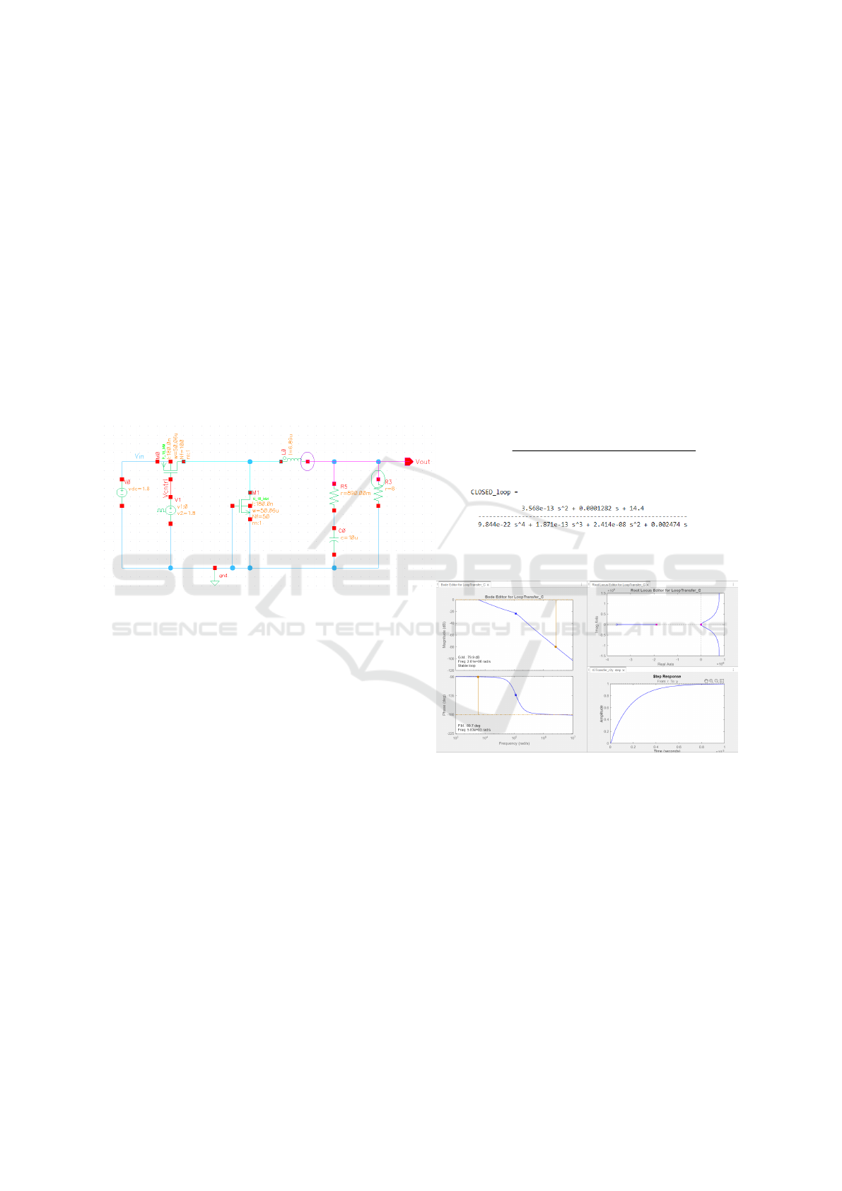
Figure 2: Closed loop transfer function of type2
Figure 3: TYPE-II MATLAB result
Following the error amplifier, a comparator com-
pares the error signal with a ramp signal . The out-
put of the comparator is a PWM signal, where the
duty cycle is proportional to the magnitude of Ver-
ror. This PWM signal drives the MOSFETs to reg-
ulate the output voltage. PWM signals often exhibit
irregularities due to variations in the ramp signal or
the control voltage. To address this, a driver circuit
is employed. The driver circuit consists of multiple
buffers, which amplify the PWM signal to ensure it
has sufficient strength to drive the gates of the MOS-
FETs. This step is crucial for maintaining efficient
switching and minimizing power losses. The circuits
of compensators, error amplifier, comparator, driver
were designed according to the requirement and were
Design and Layout of DC-DC Buck Converter
765
integrated and was simulated.
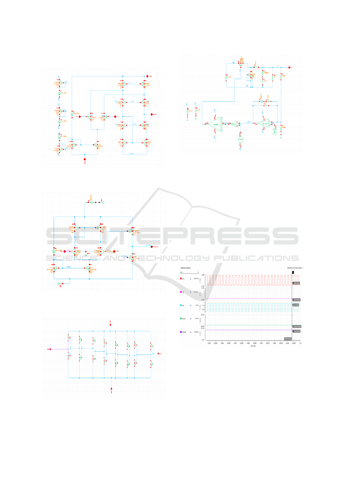
Figure 4: Error Amplifier
Figure 5: Comparator
Figure 6: Driver Circuit
Figure 7: Closed loop Buck converter circuit
5 RESULTS AND DISCUSSIONS
Initially, the open-loop configuration of the circuit
was simulated, and the corresponding results were
thoroughly analyzed to understand its behavior and
performance metrics. Following this, the feedback
network was incorporated into the design to enable
closed-loop operation, and a detailed analysis of the
system’s behavior under feedback control was con-
ducted, as illustrated in the accompanying figure. Fi-
nally, the performance table provides a concise sum-
mary of the key parameters and performance metrics,
calculated based on the derived simulation results and
observations.
Figure 8: Open loop Buck converter results
The layout was designed for the remaining cir-
cuits after excluding the filter components (inductor
and capacitor) and the compensator, as these compo-
nents were selected to be off-chip.
INCOFT 2025 - International Conference on Futuristic Technology
766
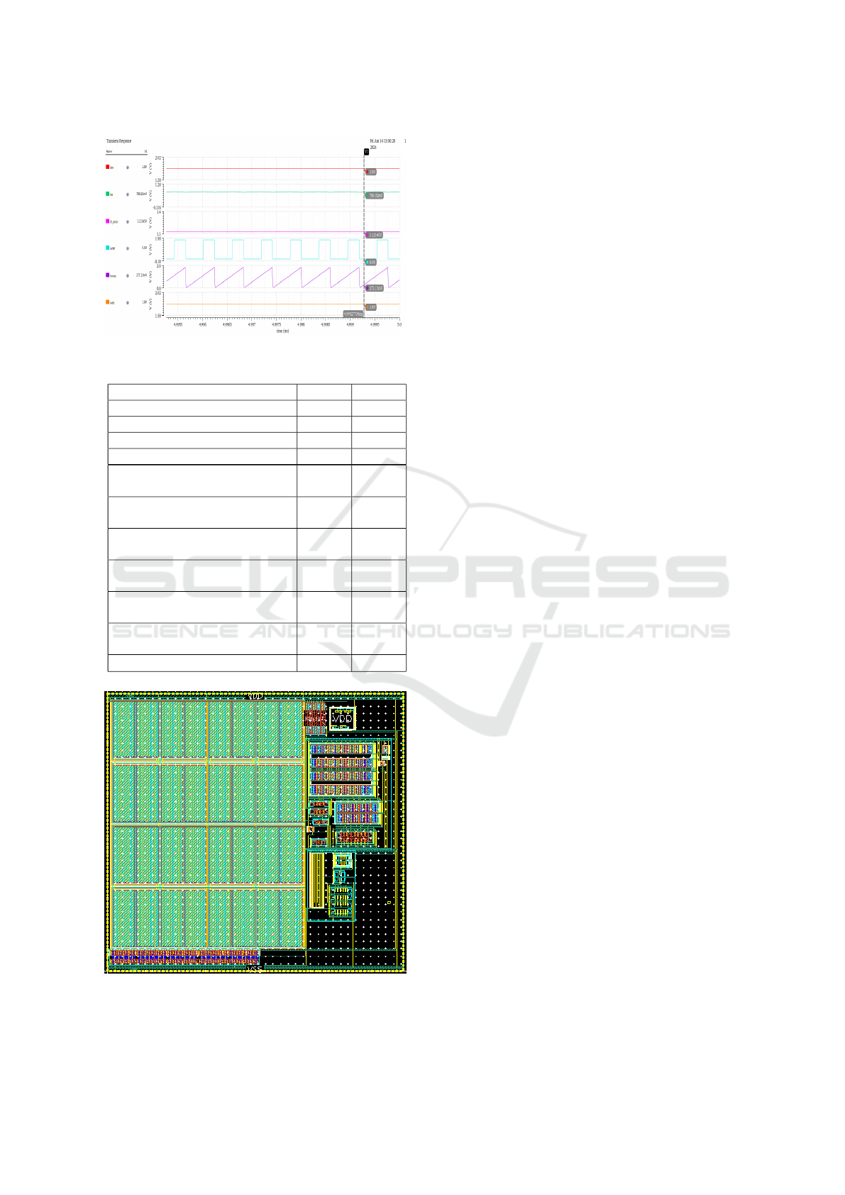
Figure 9: Closed loop Buck converter results
Table 2: Performance Summary
Parameter Value Unit
Process technology 180 nm
Input voltage, (V
in
) 1.8 V
Output voltage, (V
out
) 0.8 V
Load current, (I
Load
) 100 mA
Line transient response over-
shoot
207.475 mV
Line transient response under-
shoot
98.75 mV
Line transient response settling
time
3.089 ms
Load transient response over-
shoot
314 mV
Load transient response under-
shoot
340 mV
Load transient response settling
time
10 µs
Area 23024 µm
2
Figure 10: Buck Layout
6 CONCLUSIONS AND FUTURE
SCOPE
6.1 Conclusion
The closed-loop DC-DC converter system effectively
addresses the inherent limitations of open-loop con-
figurations by ensuring precise and stable voltage reg-
ulation across varying operating conditions. By incor-
porating an LC low-pass filter, the system minimizes
output voltage ripple, enhancing overall performance.
An error amplifier with compensator circuitry dynam-
ically adjusts the duty cycle, ensuring rapid response
to fluctuations in input voltage or load current. Ad-
ditionally, a robust PWM generation mechanism pro-
vides accurate control over the switching process, op-
timizing efficiency. The feedback mechanism forms
the backbone of the system, enabling real-time ad-
justments and ensuring stable operation even under
transient conditions. This comprehensive design ap-
proach results in a highly reliable and efficient power
conversion solution, capable of meeting the stringent
demands of modern electronic applications. This pa-
per presents the complete design, simulation, and im-
plementation of a high-frequency DC-DC step-down
converter that steps down a 1.8V input to a regulated
0.8V output at a switching frequency of 4MHz. The
converter leverages Cadence design tools and 180nm
CMOS technology, yielding successful simulation re-
sults that validate its performance. With its compact
design and efficient operation, the converter is well-
suited for power-sensitive applications such as mobile
devices, LED lighting systems, and portable electron-
ics. Moreover, the design methodology and principles
discussed in this work can be extended to other DC-
DC converter architectures, paving the way for versa-
tile power management solutions.
6.2 Future Scope
As designs incorporate more components to reduce
board size, heat management becomes a key chal-
lenge. Lower material costs are expected to improve
converter efficiency, increase operating frequencies,
and reduce sizes. With new applications, advanced
materials, and stricter energy standards, the market
for DC/DC converter modules is growing rapidly.
The future of DC/DC buck converters is especially
promising, with ongoing technological advancements
driving compact, cost-effective, and efficient power
solutions
Design and Layout of DC-DC Buck Converter
767

REFERENCES
Anvekar, S., Anusha, A. D., Giriraddi, G., Hegde, B., and
Kotabagi, S. (2024). Single stage folded-cascode op-
erational amplifier. International Journal of Microsys-
tems and IoT, 2(4):745–752.
Baharudin, N., Tunku Mansur, T. M. N., Hamid, F., Ali, R.,
and Irwanto, M. (2018). Performance analysis of dc-
dc buck converter for renewable energy application.
Journal of Physics: Conference Series, 1019:012020.
Gupta, M. and Phulambrikar, S. P. (2014). Design and anal-
ysis of buck converter. International Journal of Engi-
neering Research & Technology, 3(3):2346–2350.
Kumar, K., Praveena, V., Vijetha, J. K., Harikrishna, G.,
and Kinara, B. Design of folded cascode operational
amplifier using 1.8 micron cmos technology. Journal
of Emerging Tech.
Masri, S., Mohamad, N., and Hariri, M. H. M. (2012). De-
sign and development of dc-dc buck converter for pho-
tovoltaic application. In 2012 International Confer-
ence on Power Engineering and Renewable Energy
(ICPERE), pages 1–5.
Soheli, S. N., Aney, U. S., and Mahmud, S. I. (2021). De-
signing a highly effective dc-dc buck converter for
sustainable electronic applications. In 2021 2nd Inter-
national Conference on Robotics, Electrical and Sig-
nal Processing Techniques (ICREST), pages 178–182.
Soheli, S. N., Sarowar, G., Hoque, M. A., and Hasan, M.
(2018). Design and analysis of a dc -dc buck boost
converter to achieve high efficiency and low voltage
gain by using buck boost topology into buck topology.
pages 1–4.
Sudharshan, K., Anilkumar, C., Pallavi, R., Yatheesh, H. G.,
Santosh, and Siva Reddy, S. (2018). Design and sim-
ulation of dc-dc buck converter using cadence tool. In
2018 3rd IEEE International Conference on Recent
Trends in Electronics, Information & Communication
Technology (RTEICT), pages 2198–2202.
Tabbat, P., Babaei, E., Mohseni, P., and Marzang, V. (2020).
Study and analysis of a dc-dc soft switched buck con-
verter. IET Power Electronics, 13.
Zhang, S. et al. (2015). A 90-db dc gain high-speed nested
gain-boosted folded-cascode opamp. In 2015 11th
Conference on Ph. D. Research in Microelectronics
and Electronics (PRIME). IEEE.
INCOFT 2025 - International Conference on Futuristic Technology
768
