
A Scalable High-Speed Hybrid Full Adder Design Based on
XOR-XNOR Gates
Sukanya K
1
, Venkatram N
2
, D Devi Vara Prasad
3
, Y Jaipalreddy
4
, A Prashanth
5
and V T Ram Pavan Kumar M
6
1
Department of ECE, TKR College of Engineering and Technology, Meerpet, Hyderabad, India
2
Department of ECE, KL University, Guntur, Vijayawada, India
3
Department of EEE, PSCMR College of Engineering and Technology, Vijayawada, AP, India
4
Department of ECE, Narasaraopeta Engineering College, Palnadu, Andra Pradesh, India
5
Department of ECE, Institute of Aeronautical Engineering, Dundigal, Hyderabad, India
6
Department of Computer Science, Kakaraparti Bhavanarayana College, Vijayawada, AP, India
Keywords: Cadence, FINFET Technology, XOR-XNOR Gates, Hybrid Full Adder, CMOS.
Abstract: XOR-XNOR-based Full-swing Adder that is scalable and FinFET is described in this report. FinFET
technology has been employed as an alternative to bulk CMOS in ultra-low power designs since it offers several
advantages such as more effective channel management, reduced energy consumption, faster switching, and
so on. Previous research has compared the influence of this new technology on the circuit and evaluated the
performance gains that may be obtained. In comparison to the suggested adders, the state of the art comprises
certain known adders in FinFET technology. The suggested full adders improve Silicon area by 19.35 percent,
Average Power by 33.59 percent, Propagation Delay by 36.15 percent, Area Delay Product (ADP) by 56.22
percent, and Power Delay Product by 57.59 percent as compared to the previous full Adder. Compared to the
Mirror CMOS full adder Furthermore, performance characteristics had been investigated. By increasing the
in the extended adder structures, Full Adders to 32 bits are used without the addition of level restoring buffers
In-between stages. According to the modelling results, the planned full adder and 5 of the 11 current full adders
can be increased to 32 bits in practice. The suggested full adder outperformed the competition. The 32-bit mode
of operation the suggested hybrid full adder can be more effective due to its improved features and it can be a
more stable and superior option than present full adders.
1 INTRODUCTION
Modern electronic gadgets must operate quickly and
have a long battery life while having the lowest
feasible footprint. Portability is also considered to be
a major requirement in electronic devices. In battery-
powered systems, the quantity of energy stored in the
battery is fixed. As a result, energy dissipation is a
critical aspect in battery-powered gadgets in order to
extend the battery's average lifetime. Low-power
circuits are predicted to use smaller batteries, be
lighter, and last longer. Energy dissipation is also
critical in deep sub- micron technologies.
Developments in fabrication technology of CMOS
get larger the number of transistors in every 2 years
according to Moore’s laws, as a result the amount of
electricity dissipated per unit area increases, causing
the chip area of the circuit to expand. Excessive heat
reduces the circuit designer's dependability and
lifespan. In some cases, Low-power, high-
performance circuits may be impossible to achieve.
using complementary metal oxide semiconductor
logic.
As a result, several other devices, such as
FINFETs and CNTFETs, are being added to enhance
speed, power consumption, and area. The FinFET
transistor is one of the most significant in this field.
Introduction to VLSI: By combining several
transistors generated on circuits into a single chip,
VLSI is a method of creating integrated circuits.
VLSI was born and during the development of
sophisticated semiconductor and communication
technologies in the 1970s. A VLSI device is the
microprocessor. The microprocessor is a VLSI
K, S., N, V., Devi Vara Prasad, D., Jaipalreddy, Y., Prashanth, A. and Ram Pavan Kumar M, V. T.
A Scalable High-Speed Hybrid Full Adder Design Based on XOR- XNOR Gates.
DOI: 10.5220/0013594000004664
Paper published under CC license (CC BY-NC-ND 4.0)
In Proceedings of the 3rd International Conference on Futuristic Technology (INCOFT 2025) - Volume 2, pages 429-434
ISBN: 978-989-758-763-4
Proceedings Copyright © 2025 by SCITEPRESS – Science and Technology Publications, Lda.
429

device. As chips have become more complicated,
with hundreds of millions of transistors, the phrase is
no longer as widely used as it once was. The industry
in which ever-increasing numbers of logic devices are
crammed into ever-tinier areas. Circuits that would
have taken up a lot of space on a board may now be
squeezed into a small space only a few millimeters
wide thanks to VLSI. VLSI has been around for a
great many years and is nothing new, however as a
result of developments in computer technology, there
has been a tremendous increase in the number of tools
available to build VLSI circuits. In addition,
following Moore's law, an IC's capabilities have
grown dramatically over time in terms of compute
power, space usage, and yield. People may now
incorporate various functionality into ICs as a result
of these two advancements, opening up new vistas.
Placed systems, in which intelligent devices are
embedded into common items, and ubiquitous
computing, in which little computer devices spread to
the point where even your shoes may do important
tasks, are two examples.
Designers needed methods to combine numerous
simulation levels, which is when Verilog was
developed. In the early 1980s, there were functional
simulators, switch-level simulators, and gate-level
simulators (sometimes created on the fly in software),
but no easy technique to connect them. In addition,
traditional programming languages were/are
primarily sequential, making them "semantically
problematic" for simulating the concurrency of digital
circuitry. Phil Moore of Gateway Design Automation
invented Verilog in 1983-4, and a year later, the first
simulator was developed.
2 LITERATURE SURVEY
Analysis of Hybrid Full Adders Using Logical
Effort
The advantages of hybrid full adders are explored
in this work, and hybrid full adders are also contrasted
with traditional CMOS circuits. Compared to
traditional CMOS circuits, Hybrid Full Adders
Utilizing Logical Effort structures are faster and use
less power. (Kumar, Gotam, et al. 2017), (Naseri,
Timarchi, et al. , 2017), (Rajagopal, Chakrapani, et al.
2021), (Kandpal, Tomar, et al. 2020), (Hasan, Islam,
et al. 2021)
XOR-XNOR module is used in a scalable high-
speed hybrid 1-bit full adder architecture:
In this study, full adders based on XOR-XNOR
are built, as well as compared with hybrid FA circuits
based on XOR-XNOR, with outstanding results that
allow these FAs to be used in digital arithmetic blocks
of contemporary microprocessors.
Design of XOR-XNOR Topology Low Power
High Speed Complete Adder Circuits: In this paper
advantages of the full adders are discussed with the
real time applications. (Wairya, 2012), (Jyothi, Rao,
et al. 2020), (Subhashini, Kamaraj, et al. 2019),
(Addagatla, Chelle, et al. 2022), (Prashanth, et al.
2022)
Introduction to FIN-FET:
A Fin field effect transistor is something of a
transistor. It serves as both an amplifier and a switch
because it is a transistor. Home PCs, laptops, tablets,
smartphones, wearable technology, high-end
networks, automobiles, and other gadgets are only a
few of its applications. A fin-shaped field-effect
transistor is referred to by the abbreviation "fin field
effect transistor.". The name "fin" refers to the fin-
shaped body of the transistor, which is distinguished
by the silicon fin that serves as the main body. Field-
effect because an electric field controls the
conductivity of the substance. A Fin field effect
transistor is a device that does not have a single plane.
It is sometimes referred to as 3D since it has a
third dimension. (Prashanth, Sree, et al. 2023),
(Raghunandan, Shilpa, et al. 2019), (Kadu, Sharma,
et al. 2017), (Taherinejad, Abrishamifar, et al. 2009),
(Balakumaran, Prabhu, et al. 2016), (Ramkumar,
Gracin, et al. 2020)
Figure.1: Structure of FINFET
3 CIRCUITS OF XOR, NOR AND
FULL ADDER
The Basic binary circuits used for the designs are
briefly explained here.
INCOFT 2025 - International Conference on Futuristic Technology
430
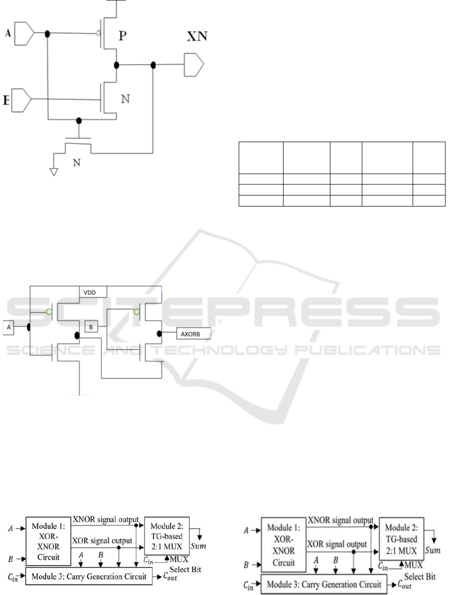
Figure 2: Circuits of XOR, NOR and Full Adder
The output of an XOR circuit is always 1 when the
input is logic 1, and it is always 0 when the input is
logic 01 or logic 10. Moreover, the output logic is
always 0 when the input logic is 11.
3.1 XNOR circuit
Figure-3: Schematic of XNOR
When the input is logic 0 0 for the XNOR circuit then,
the output is logic is 1 and when the input is logic 01
or logic 10, then the output is logic is always 0. And
when the input logic is 11 then the output logic is
always 1.
3.2 Existing Models
Figure 4: Schematic of Design-I
Here 3 blocks are combined together to form
hybrid full adder circuit i.e., module-1 XOR-XNOR
circuit, module-2 TG based 2:1 mux, module-3 carry
generation circuit. And also, the output bits are A, B,
Cin, and sum. It is composed of an XOR-XNOR
module and a TG-based module that together provide
the sum result and a separate carry generating module
that accepts input from the XOR-XNOR module to
give Cout output.
Table. 1. Existing CMOS models: Proposed Design
Simulation Result
Supply
Voltage
(V)
CCMOS
Power
(uw)
Delay
(PS)
Proposed
Power(uw)
Delay
0.6V 0.8 40.8 0.38 43.4
0.8V 1.1 54.6 0.54 40.3
1V 1.28 60.3 0.85 38.5
3.3 Introduction to Cadence Tool
Cadence is a renowned EDA and semiconductor
IP company. cadence allows engineers to produce the
standard cells, IP blocks, and transistors needed in
SoCs using custom/analog tools. In the most recent
semiconductor processing nodes, our digital
technologies automate the creation of giga - scale,
gigahertz SoCs and their verification. IC packaging
and PCB tools may be used to design our Whole
Boards and Subsystems. Cadence also has a
developing IP portfolio for memory, interface
protocols, and verification.
The user interface in Cadence is visual, including
windows, forms, and menus. DFW's primary windows
are as follows: The environment is controlled through
the Command Interpreter Window (CIW). It also acts
as a log window for many of the tools that may be
started from here. The Library Manager displays the
design libraries and the many buildings found inside
them. The current design is displayed in the Design
Window (DW). It is possible to have more than one.
DW opened simultaneously with various (or the
same) tools.
TW (Text Window) displays text. It might be a
requested log or report, or copy editor.
Figure 5. The design flow in cadence is as follows
A Scalable High-Speed Hybrid Full Adder Design Based on XOR- XNOR Gates
431

Figure .6. The design flow of cadence tool
4 PROPOSED DESIGNS
4.1 Design-1:
In this part, a brief explanation of the design of the
XOR-XNOR-based hybrid full adder circuit's
suggested block diagram is provided.
Here 3 blocks are combined together to form
hybrid full adder circuit i.e., module-1 XOR-XNOR
circuit, module-2 TG based 2:1 mux, module-3 carry
generation circuit. And also, the output bits are A, B,
Cin, and sum. It is composed of an XOR-XNOR
module, a TG-based module, which produces the sum
output, and a separate carry generating module, which
takes input from the XOR-XNOR module and
produces Cout output.
Figure.7 single bit full adder Simulation Test bench.
The FINFET-based transmission gates are used in
the design-II schematic illustrated in Figure 7. For the
proposed XOR circuit, the following requirements
must be met.
Conditions:
I: If A = 0 and B = 0, then XOR = B=0 (since B = 0).
II: If A = 0 and B = 1, then XOR = B = 1 (since B =
1).
III: If A = 1 and B = 0, then XOR = A=1 (since A =
1).
IV: If A = 1 and B = 1, XOR = Gnd.
P5 and p6 switch on permitting weak logic 0 to go
in the direction of the XOR node for requirement 1 of
the formation of an XOR signal (since PMOS passes
weak logic 0). n6 has been utilized to tackle this
problem and offer solid rationale. In condition 1, A =
0, and p7 is activated. As a response, logic 1 is
assigned to the intermediate node I. This logic 1 of
Inactivates n6, which sends strong logic 0 to the XOR
node (since NMOS passes strong logic 1).
Table. 2. operation Table of XOR circuit
Pattern no
Input
side A
b
Complete
transistor
path
transistor
route
without a
full
swin
g
output signal
or logic on
the output
side
1. 1 1
GND GND=0
2. 1 0
A A=1
3. 0 1
B B=1
The suggested XNOR circuit is subject to the
following
I: If A = 0, and B = 0, then XNOR = Vdd.
II: If A = 0 and B = 1, XNOR = A.
III: If A = 1 and B = 0, XNOR = B.
IV: If A = 1 and B = 1, XNOR = B.
Figure. 8: Carry circuit
INCOFT 2025 - International Conference on Futuristic Technology
432

Table. 3: Operation Table of sum and carry circuits
Cin
Input
pattern
A
B Cout SUM
one one one one one
one zero one zero
zero one 1 0
0 00 1
0 one one one 0
one o 0 one
0 one 0 one
0 o0 o
If Cin = 0, Total = XOR (A XOR B).
If Cin = 1, Total = XOR (A XOR B) The Carrier
Circuit's Conditions, If Cin is 0 then A=0 and B=0
then output will be Cout is 0 and sum is 0.
Condition:2.If Cin is 0 then A=0 and B=1 then
outputs will be Cout is 0 and sum is 1. condition:3. If
Cin is 0 then A=1 and B=0 then outputs will be Cout
is 0 and sum is 1.
V: If Cin is 0 then A=1 and B=1 then outputs will
Figure 9: Depicts the NOR circuit's output
Figure 10: depicts the XNOR circuit's output
Figure 9 depicts the XOR circuit's output
waveform. The same as explained in the table-4.1 of
chapter-4. When the input logic is 0 0 for the XOR
circuit then, the output logic is 0 and when the input
logic is 01 or logic 10, then the output logic is always
1. And when the input logic is 11 then the output logic
is always 0. waveform. is the same as explained in the
table-4.2 of chapter-4. When the input logic is 0 0 for
the XNOR circuit then, the output logic is 1 and when
the input logic is 01 or logic 10, then the output logic
is always 0. And when the input logic is 11 then the
output logic is always 1.
5 RESULTS AND CONCLUSIONS
The scalable high-speed hybrid full adder based on
XOR-XNOR gates' simulation results demonstrate
how successful it is in terms of shorter propagation
delays, lower power consumption, and compact
design. These characteristics make it appropriate for
energy-efficient and high-performance applications,
particularly in digital circuits that need quick
arithmetic operations.
An inventive idea in digital circuit design is a
scalable, fast hybrid full adder architecture built on
XOR-XNOR gates. These designs seek to maximize
performance parameters that are essential for
contemporary computer systems, such as speed, area,
and power consumption.
REFERENCES
Rajeev Kumar, Sandeep Gotam and S. Vikram Singh “A
new full-adder design using XNOR- XOR Circuits: A
Review,” in proceedings of 2017International
Conference on Emerging Trends in Computing and
Communication Technologies (ICETCCT) November
2017.
Hamed Naseri., and so Timarchi “Low-Power and Fast Full
Adder by Exploring New XOR and XNOR Gate,” in
proceedings of the April 2018 IEEE Transactions on
Very Large-scale Integration (VLSI) Systems, Chennai,
India, March 2325,2017.
Thiruvengadam Rajagopal1·Arvind Chakrapani, “Design
of Ternary Logic Circuits Using CA Nov l High-
Performance Hybrid Full Adder for VLSI Circuits, “in
proceedings of the November 2021 Circuits Systems
and Signal Processing.
Jyoti Kandpal, and Abhishek Tomar, Mayur Agarawal,
Kamal KUMAR Sharma, “High- Speed Hybrid-Logic
Full Adder Using High-Performance 10-T xor-
xnorCell,” in proceedings of the April 2020 IEEE
Transactions on Very Large-Scale Integration (VLSI)
A Scalable High-Speed Hybrid Full Adder Design Based on XOR- XNOR Gates
433

Systems Published by Institute of Electrical and
Electronics Engineers.
Mehedi Hasan, Sharnali Islam, Mainul Hossain, Hasan U.
Zaman “A scalable high-speed hybrid 1-bit full adder
design using XOR-XNOR module” in proceedings
other First 22 July 2021.
Subodh Wairya, “Comparative Performance Analysis of
XOR-XNORFunctionBased High-Speed CMOS Full
Adder Circuits for Low Voltage VLSI Design,” April
2012 International Journal of VLSI Design and
Communication Systems3(2):221242
DOI:10.5121/vlsic.2012.321.
Challa Lakshmi Jyothi, S Hanumantha Rao, “Novel Design
of Low-Power Highspeed Hybrid Full Adder Design
using Gate Diffusion Input (GDI) Technique,” in
proceedings of n October 10,2020. | PP: 323-328 |
Volume-9 Issue-12, October 2020.
T. Subhashini, M. Kamaraj, K. Babulu, “Low-Power and
Fast Adders Using XOR and XNOR Gates” in
proceedings International Journal of Engineering
Research and Technology. ISSN 0974- 3154, Volume
12, Number 12 (2019), pp. 2072-2076 International
Research Publication House.
Prashanth Addagatla and Radhika, Chelle and Keerthana,
Nagasani, Power Saving System Based on Visitor
Count and Light Sensing with Arduino (February 16,
2023). Proceedings of the International Conference on
Innovative Computing & Communication (ICICC)
2022, Available at SSRN:
https://ssrn.com/abstract=4361280
Addagatla Prashanth, Emotion Recognition in Speech
Using MFCC Proceedings of the International
Conference on Computational Vision and Bio-Inspired
Computing, Vol 1420, issue 2. 31 March 2022,
Publisher Name Springer, Singapore, Print ISBN978-
981-16-9572-8 DOI https://doi.org/10.1007/978-981-
16-9573-5_14.
Addagatla Prashanth, Rahul Sree, Niharika Implementation
of a Smart Patient Health Tracking and Monitoring
System Based on IoT and Wireless Technology
Proceedings of the International Conference on
Advances in Intelligent Systems and Computing book
series (AISC, volume 1442) 01 June 2023 Publisher
Name Springer, Singapore, Print ISBN978-981-99-
0549-2 DOI: https://doi.org/10.1007/978-981-99-0550-
8_23
A. Raghunandan and D. R. Shilpa, "Design of High-Speed
Hybrid Full Adders using FinFET 18nm
Technology," 2019 4th International Conference on
Recent Trends on Electronics, Information,
Communication & Technology (RTEICT), Bangalore,
India, 2019, pp. 410-415, doi:
10.1109/RTEICT46194.2019.9016866.
C. P. Kadu and M. Sharma, "Area-efficient high-speed
hybrid 1-bit full adder circuit using modified XNOR
gate," 2017 International Conference on Information,
Communication, Instrumentation and Control
(ICICIC), Indore, India, 2017, pp. 1-5, doi:
10.1109/ICOMICON.2017.8279064.
N. Taherinejad and A. Abrishamifar, "A new high speed,
low power adder; using hybrid analog-digital
circuits," 2009 European Conference on Circuit Theory
and Design, Antalya, Turkey, 2009, pp. 623-626, doi:
10.1109/ECCTD.2009.5275072.
R. Balakumaran and E. Prabhu, "Design of high speed
multiplier using modified booth algorithm with hybrid
carry look-ahead adder," 2016 International
Conference on Circuit, Power and Computing
Technologies (ICCPCT), Nagercoil, India, 2016, pp. 1-
7, doi: 10.1109/ICCPCT.2016.7530164.
E. Ramkumar, D. Gracin, P. Rajkamal, B. P. Bhuvana and
V. S. Kanchana Bhaaskaran, "Design and Analysis of
Low Power and High Speed FinFET based Hybrid Full
Adder/Subtractor Circuit (FHAS)," 2020 IEEE
International Symposium on Smart Electronic Systems
(iSES) (Formerly iNiS), Chennai, India, 2020, pp. 281-
284, doi: 10.1109/iSES50453.2020.00069.
M. Shruthi, A. Prashanth and S. Bachu, "Machine Learning
and End to End Deep Learning for Detection of Chronic
Heart Failure from Heart Sounds," 2024 5th
International Conference on Recent Trends in
Computer Science and Technology (ICRTCST),
Jamshedpur, India, 2024, pp. 310-316, doi:
10.1109/ICRTCST61793.2024.10578348.
P. S. Reddy, A. Prashanth and S. Bachu, "An FPGA based
Scheme for Real-Time Max/Min-Set-Selection
Sorters," 2024 1st International Conference on
Cognitive, Green and Ubiquitous Computing (IC-
CGU), Bhubaneswar, India, 2024, pp. 1-5, doi:
10.1109/IC-CGU58078.2024.10530671.
Trapti Sharma, Addagatla Prashanth, Srinivas Bachu,
Deepa Sharma, Anil Kumar Sahu, Efficient design
approaches to model CNTFET-based Ternary Schmitt
Trigger circuits, AEU - International Journal of
Electronics and Communications, Volume
173,2024,155031, ISSN 1434-8411,
https://doi.org/10.1016/j.aeue.2023.155031.
N. K. Niranjan, R. B. Singh and N. Z. Rizvi, "Parametric
analysis of a hybrid 1-bit full adder in UDSM and
CNTFET technology," 2016 International Conference
on Electrical, Electronics, and Optimization
Techniques (ICEEOT), Chennai, India, 2016, pp. 4267-
4272, doi: 10.1109/ICEEOT.2016.7755523.
G. Likhitha, D. V. Raju, R. S. Naveen and T. Zaid,
"Implementation of High-Speed Full Adder Using
XOR XNOR Cell in FinFET Technology," 2024 10th
International Conference on Advanced Computing and
Communication Systems (ICACCS), Coimbatore,
India, 2024, pp. 1663-1667, doi:
10.1109/ICACCS60874.2024.10716943.
Creation and Assessment of Herbal Gel with Guava Leaf
Extract K. Deepika, A. Sairoja and P. Sri Jyothi E3S
Web Conf., 564 (2024) 07003. DOI:
https://doi.org/10.1051/e3sconf/202456407003.
INCOFT 2025 - International Conference on Futuristic Technology
434
