
A New and Adaptive Power Gating Technique in Full Adder
Abhishek Nag
a
,
Arka Chakraborty
b
, Vivek Kumar Singh
c
and Sambhu Nath Pradhan
d
Department of Electronics and Communication Engineering, National Institute of Technology Agartala, India
Keywords: Power Gating, Body Biasing, Sleep Transistor, Standby Power, CMOS.
Abstract: Power gating has proven to be one of the more effective techniques of reducing leakage power in VLSI
Circuits and systems. This paper introduces a new and dynamic power gating strategy in Full adder circuits.
The proposed method creatively uses sleep transistors to turn off the main Adder circuit only for specific input
combinations, saving standby power. The designed Adder circuits are based on static CMOS logic, and are
simulated in CADENCE Virtuoso tool at 45 nm technology. The simulation results indicated a maximum
leakage power savings of 74% and total power savings of 33.6% after implementation of the proposed
technique, with a nominal increase in area overhead and delay. abstractshould summarize the contentsof the
paper and shouldcontain atleast70and atmost200 words. It should be set in 9-point font size, justified and should
have a hanging indent of 2-centimenter. There should be a space before of 12-point and after of 30-point.
1 INTRODUCTION
Power consumption has increased as a result of
increased packing density, which allows more gadgets
to be crammed into smaller spaces. In an effort to
increase the power efficiency of the systems, new
methods have been developed. One such method is
power gating [1, 2, 3], which involve briefly shutting
off the entire circuit when it is not in use. To put the
circuit in sleep mode and save standby power, sleep
transistors are utilized. In industries, this method is
frequently employed to lower circuit power usage.
This work considers introduction of a novel power
gating strategy in Adder circuits to reduce the leakage
power consumption. Numerous prior works have been
carried out in reducing power consumption of Adder
circuits [4, 5, 6, 7, 8]. Majority of the earlier works
considers employing a hybrid XOR-XNOR
architecture to design the adder [4, 5, 6]. The hybrid
Adder circuit developed utilizes much lesser
components compared to standard CMOS logic,
however, leads to reduction of full-swing outputs
when used in a cascaded circuit. Other works in
reducing power consumption of Adders uses GDI
logic [7, 8] and has successfully resulted in reducing
a
https://orcid.org/0000-0002-1836-1547
b
https://orcid.org/0009-0007-2775-2850
c
https://orcid.org/0000-0003-4614-7633
d
https://orcid.org 0000-0002-5461-6535
overall power. However, the issue with GDI logic is
again a low swing output, which needs correction.
CMOS logic, although requires more components to
design a circuit, provides perfectly full swing output,
and has turned out to be much more reliable compared
to other hybrid designs in terms of its robustness and
scalability [9].
This manuscript introduces a new power gating
logic in CMOS based Full adder circuit, which
autonomously switches off the power supply
connection to the Full Adder for certain specific input
conditions. The resultant gated logic also employs
variations of Body biasing in the NMOS, and its effect
on total power dissipation is reported. The simulation
results indicate a maximum leakage power savings in
the full adder to be approximately 74%, with an area
overhead of 14.2%. To analyze the versatility of the
logic, the power gating strategy is compared with
several optimized Full Adder circuits proposed in prior
works and their detailed results are reported in section 4.
2 LITERATURE REVIEW
Much effort has been made in the last few decades to
Nag, A., Chakraborty, A., Singh, V. K. and Pradhan, S. N.
A New and Adaptive Power Gating Technique in Full Adder.
DOI: 10.5220/0013320700004646
In Proceedings of the 1st International Conference on Cognitive & Cloud Computing (IC3Com 2024), pages 99-105
ISBN: 978-989-758-739-9
Copyright © 2025 by Paper published under CC license (CC BY-NC-ND 4.0)
99
lower the power consumption of VLSI circuits. Both
dynamic power and static power dissipation
contribute to the overall power consumption of a
circuit. This section presents a brief overview of the
various types of power dissipation and steps that can
be adopted to reduce them.
2.1. Dynamic Power Dissipation
Dynamic power dissipation occurs during runtime of
a circuit and is basically categorized as switching
power and short circuit power. Majority of the total
power consumption of a circuit is contributed by
dynamic power.
Switching power – Switching Power dissipation
occurs when a circuit transitions between ‘ON’ and
‘OFF’ state [10]. The circuit dissipates more dynamic
power when transistors are made to switch states more
frequently. Clock gating techniques [11], in which the
clock feeding the flip-flop and memory elements is
briefly turned off while not in use for the ongoing
computation, are employed to reduce this component
of leakage power. As a result, less needless switching
do not occurs, which lowers dynamic power
dissipation. Another widely used technique to reduce
switching power is by adopting voltage scaling [12].
Short circuit power – In a CMOS circuit, at any given
time, the pull-up or pull-down network is conducting.
As a result, a direct conductive path from VDD to
GND cannot emerge. As a result of the delay in the
signal propagating from transistor to transistor, a
conductive channel from ground GND to voltage
source VDD may, nonetheless, briefly form during
switching. This causes a sharp increase in current and
adds to the circuit's overall power loss. The most
popular techniques of reducing short circuit power is
by reducing device size [13] or increasing threshold
voltage of the transistors [14].
2.2 Static Power Dissipation
Even in the off state, undesired currents are still
passing through the transistors in a circuit. This is
mostly because, even before the gate voltage
surpasses the threshold voltage, there is a partial
inversion layer present in the channel beneath the
gate, resulting in sub-threshold conduction [15]. One
of the most efficient technique of reducing static
power (also referred to as leakage power) is power
gating [16, 17]. By virtue of power gating, unused
portions of a circuit are disconnected from supply
power. The basics of power gating technique are
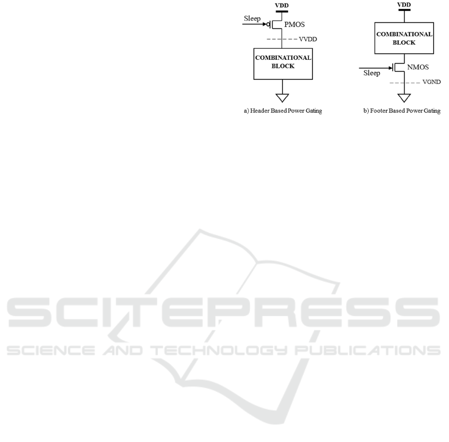
shown in Fig. 1.
Fig. 1. Basic Power Gating Implementation Techniques
Power gating technique can be classified into two
types:-
a. Header Based Power Gating: In this technique,
the supply voltage (VDD) is connected to the main
circuit through a header PMOS transistor, referred to
as sleep transistor {Fig. 1(a)}. A virtual VDD
(VVDD) now acts as the supply voltage to the circuit.
The gate input to the sleep transistor, called sleep
signal, decides the criteria for either cutting off the
power supply to the circuit or allowing it. The
challenge for circuit designers is to develop a
efficient way of generating the sleep signal, without
hampering the circuits performance.
b. Footer Based Power Gating: In this technique, the
connection of a circuit to GND is carried out through
a NMOS footer transistor {Fig. 1(b)}. The purpose of
the footer transistor is to disconnect the connection to
GND during periods of inactivity of the circuit,
subsequently saving unnecessary leakage power
dissipation.
3 PROPOSED POWER GATİNG
TECHNİQUE IN FULL
ADDER
A standard static CMOS Full adder circuit is
considered initially in this approach for
implementation of the proposed power gating logic.
The basic schematic diagram of a conventional CMOS
full adder along with its truth table is presented in Fig.
2.
IC3Com 2024 - International Conference on Cognitive & Cloud Computing
100
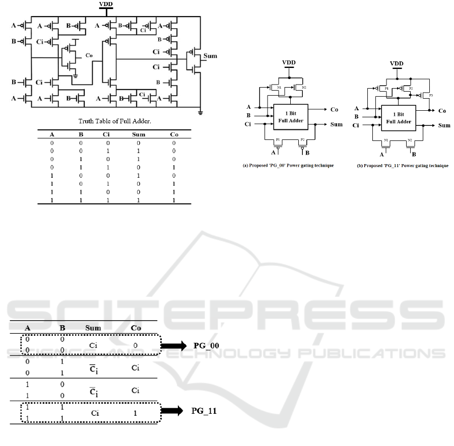
Fig. 2. Conventional Static CMOS Full Adder Circuit and
its Truth Table.
The theory of the proposed gating strategy is to
disconnect the Full adder circuit from VDD during
period of inactivity. The inactive period information
is extracted from the truth table of the Full adder, as
depicted in following Fig. 3.
Fig. 3. Extraction of Power Gating Criteria in Full Adder.
The truth table of the full adder is represented in a
minimized form in Fig. 3. Here, the sum output of the
adder is realized in terms of input ‘Ci’, whereas, ‘Co’
output is realized in terms of 0, 1 & ‘Ci’. Based on
the minimized Table, 2 different power gating criteria
are established for the full adder, represented as
follows:
PG_00: A = B = 0 => Sum = Ci & Co = 0
PG_11: A = B = 1 => Sum = Ci & Co = 1
It can be deduced from the above two criterias that
when A & B input of the Adder are equal, the Sum
output tends to be same as the Carry in input ‘Ci’,
and subsequently the Adder circuit functioning is
non-essential during this states. The proposed gating
logic in this work is established separately for both
the above criteria, shown in Fig. 4.
Fig. 4. Proposed Power Gating Techniques in Full Adder.
a. PG_00 Power gating technique: This
technique is shown in Fig. 4 (a), which
considers the implementation of Power
gating during the input combination A = B =
0. During this state, it can be observed that
Sum = Ci whereas Co becomes 0. Hence,
operation of the entire adder block is non-
essential during this combination. The gated
architecture shown in Fig. 4 (a) automatically
disconnects the power supply to the Adder
during this input combination and
concurently connects the input Ci to the Sum
output. The power gating is carried out
through the two sleep transistors N1 & N2,
whereas the bypass logic of connecting Ci to
Sum output is executed by P1 and P2.
For the other input combinations, the adder
will work normally, however, since NMOS
sleep transistor are used, the supply voltage
at Virtual VDD will be lesser compared to
VDD since NMOS is a ‘weak 1’. This will
result in higher leakage savings, but at the
same time, the output swing will reduce for
the Sum & Co.
b. PG_11 Power gating Technique: This
technique is shown in Fig. 4 (b), which
considers the implementation of Power
gating during the input combination A = B =
1. During this state, it can be observed that
Sum = Ci whereas Co becomes 1. Similar to
the PG_00 technique, the Full adder circuit
can be power gated during this combination.
However, to obtain High output at the Co
node, an extra pull up transistor P3 is
introduced in the design. The issues occuring
A New and Adaptive Power Gating Technique in Full Adder
101

in PG_00 technique is overcome to a large
extent in PG_11. In PG_11, PMOS sleep
transistors (P1 and P2) are used for power
gating, and subsequently, proper supply is
observed at Virtual VDD node. The virtual
VDD node is connected as the Gate input of
the pull up transistor P3, switching ‘ON’ the
P3 transistor only when the Full Adder
circuit is power gated i.e Low value at
virtual VDD. However, during power
gating, it may occur sometimes that some
intermediate charge remains at the virtual
VDD node for some time, which will delay
the activation of P3. To correct this issue, the
width of the transistor P3 is increased. The
NMOS transistors (N1 & N2) are used as
bypass transistors to connect the input Ci to
Sum output only during Power gating state
i.e. A = B = 1. The use of extra transistor in
this technique reduces the overall power
savings compared to PG_00 technique,
hence, a positive body biasing technique is
also introduced in this technique to further
reduce the leakage power.
The NMOS bypass transistors ‘N1’ & ‘N2’ in Fig. 4
(b) are positively body biased to further reduce the
leakage power of PG_11 technique. Authors in [18]
have described the effects of body biasing the NMOS
on power dissipation and delay of the circuit. When
the body (substrate) of the NMOS is positive biased
(connected with VDD), the p-type substrate gets
flooded with majority charge carriers i.e., holes. This
leads to two scenarios: -
a. First of all, the body-source junction
becomes forward biased due to positive
biasing of the body. This leads to increase in
junction current and hence the power
dissipation increases. To avoid this
phenomenon that leads to increase in power
dissipation, the body of NMOS is generally
connected to the ground.
b. The second phenomenon that is the result of
positive body biasing is, due to the increase
in majority charge carriers in the substrate
i.e., holes, the number of minority charge
carriers decreases (mass-action law: n*p =
n
i
2
). This reduces the sub-threshold
conduction resulting in the reduction of the
net power consumption of the circuit.
However, the reduction in the power
becomes smaller as the channel length keeps
on decreasing, as it increases the short
channel effects drastically.
4 SIMULATION RESULTS AND
DISCUSSIONS
The design and simulation of Adder circuits are carried
out in CADENCE virtuoso tool at 45 nm technology.
All simulations are carried out at 1.8 V power supply
at T = 270 C. The detailed simulation waveforms for
the standard CMOS Full adder as well as Power gated
Full adders (PG_00 & PG_11) are shown in Fig. 5.
Fig. 5. Simulation waveforms of standard and proposed
power gated Full Adders.
The leakage power results of the Static CMOS Full
Adder (SCFA), PG_00 & PG_11, considering all
possible input combinations is presented in the
following Table 1.
Table 1. Leakage power analysis of the Full Adders.
Inputs Leakage Power (pW)
Savings
compared to
SCFA (%)
A B Ci SCFA PG_00 PG_11 İn
PG_00
In
PG_11
0 0 0 168.4 43.7 163 74 3.2
0 0 1 .168.3 47.9 162.4 71.5 3.5
0 1 0 172.1 154.5 177.6 10.2 -3.2
0 1 1 173 157.2 182.3 9.1 -5.4
1 0 0 170.6 147.5 167 13.5 2.1
1 0 1 170.7 150.8 167.1 11.6 2.1
1 1 0 166.4 151.5 58.9 8.9 64.6
1 1 1 166.2 149.2 61.1 10.2 63.2
It can be observed from the Table that a maximum
leakage power savings of 74% is achieved in PG_00
technique, whereas, PG_11 technique resulted in
maximum leakage savings of 64.6%. Negative sign
in the Table indicates that power consumption
increased after the implementation of proposed
gating technique.
IC3Com 2024 - International Conference on Cognitive & Cloud Computing
102

Although leakage power savings is lesser in PG_11
compared to PG_00, PG_11 technique results in
better output voltage swing. The details of the Total
power, Area & Delay Results are presented in Table
2. Input frequency of 500 MHz is considered for
simulation and the delay results are reported based on
worst-case analysis for calculating the critical path.
Area analysis is reported as an estimation approach
[16, 17, 19] and represented in terms of λ2,
considering λ as the particular technology’s feature
size. The total transistor count is multiplied by the
width of a minimum width transistor (k) to obtain the
area.
Table2.TotalPower,Area, Delay andPDPresults of the Full
Adder circuits.
SCFA PG_00 PG_11
Total Power(nW) 166 110.4 128.6
PowerReduction
w.r.t SCFA (%)
- 33.6 22.5
Area (
λ
2
) 28
k
32
k
33
k
AreaOverhead w.r.t
SCFA (%)
- 14.2 17.8
Delay (ns) 0.0416 0.0448 0.0462
Increase in Delay
w.r.t SCFA
- 7.7 11.05
PDP(J) 6.9 E-18 4.9 E-18 5.9 E-18
PDP savings w.r.t
SCFA (%)
- 28.9 14.5
It can be observed from Table 2 that maximum Total
power savings of 33.6% is achieved by virtue of
PG_00 technique implementation, whereas, PG_11
results in maximum savings of 22.5%. In terms of area
also, PG_00 provides better results by introducing an
area overhead of 14.2% compared to 17.8% in PG_11.
However, as mentioned earlier, due to reductıon in
output swing in PG_00, functıonal errors may arıse
when used in a cascaded system. Therefore, PG_00
technique is more suitable for smaller systems
compared to PG_11. The reduction of full swing in
PG_00 is overcompensated by providing better delay
results than PG_11, as can be seen in Table 2. This is
because, PG_00 uses NMOS sleep transistors, which
are comparatively faster than PMOS.
Delay in power gated systems is mainly
contributed by the wake-up time associated with the
sleep transistors for supply voltage adjustment [16,
17]. This delay can be further adjusted by increasing
the width of sleep transistor [16], however, at the
expense of lesser power savings. To analyze the
overall impact of the proposed approach, energy
calculation is carried out by reporting the Power Delay
Product (PDP) of the various Adder designs. PDP
savings up to 28.9% can be achieved by
implementation of the proposed gating logics.
For a comparative analysis, various Full Adder
Designs of prior works are considered [4, 5, 7, 20, 21,
22] and the detailed Power, Delay and PDP results
are tabulated in the following Table 3. The full adder
designs proposed in the References mentioned in
Table 3 are first of all designed in CADENCE
Virtuoso tool at 45 nm technology and simulated to
obtain the power and delay results.
Table3.Comparative analysis w.r.t prior works.
Full
Adder
Power
(nW)
Delay
(ns)
PDP (x
10
-18
J)
Reduction of
PDP w.r.t
SCFA (%)
SCFA 166 0.0416 6.9 -
PG_00 110.4 0.0448 4.9 28.9
PG_11 128.6 0.0462 5.9 14.5
[4] 112.2 0.0410 4.6 33.3
[5] 138.7 0.0391 5.4 21.7
[7] 106.4 0.0420 4.5 34.7
[20] 152.4 0.0395 6.1 11.5
[21] 118.2 0.0414 4.9 28.9
[22] 144.5 0.0529 7.6 -10.1
It can be inferred from Table 3 that the proposed
approach PG_00 achıeves better power as well as PDP
savings compared to majority of the prior works. In Ref
[4], authors introduced a hybrid XOR-XNOR circuit
for designing the Full Adder. Pass transistor logic is
adopted in designing the XOR-XNOR gates along with
a feedback concept. Although, it achieves desired
results in low frequency applications at nominal supply
voltage, however, upon application in high frequency
systems at smaller technology, timing errors are highly
likely to occur due to the shortcomings of pass
transistor logic [9]. Again, in [7], authors used a GDI
logic for designing the Full adder circuit. The basic
limitations of GDI logic is the requirement of
additional buffers for overcoming the low swing output
due to drop in threshold voltage [23]. The proposed
power gating strategy PG_00 is mainly focused in
power reduction and it has successfully achieved its
goal without significantly affecting other system
functionality. The issues arising in PG_00 are
overcome to a large extent in PG_11 technique, which
results in a proper swing output along with reducing
power dissipation. The main advantage of this
approach is its simplicity in application and its ability
to easily extend to complex cascaded Full Adder
circuits of higher bits.
5 CONCLUSION
A novel power gating mechanism is developed and
A New and Adaptive Power Gating Technique in Full Adder
103

applied for Full adder circuits in this work. In the
suggested paradigm, the primary circuit is adaptively
turned off and is deactivated only when specific input
combinations are met. The information extracted
from these combinations is utilized to develop an
activation logic using PMOS/NMOS sleep
transistors. Two different power gating logics are
introduced in this paper, namely PG_00 & PG_11.
The PG_00 approach resulted in higher power
savings but is limited by reduction in full swing
output. On the other hand, PG_11 provide proper
swing output at the expense of lesser power savings.
A maximum leakage power savings of 74% is
achieved by virtue of implementing PG_00 technique
and maximum of 33.6% savings is recorded for the
total power (Dynamic + Static). Maximum of 28.9%
PDP savings is also achieved in this work. One of the
advantages of the proposed logic is that it may be
applied to other analogous circuits constructed from
various logics, including transmission gate, pass
transistor, GSI based and so on. A detailed
comparison with prior works is reported in the paper
and is indicative of the proposed works effectiveness.
ACKNOWLEDGEMENT
This work is supported by Department of Electronics
and Communication, NIT Agartala.
REFERENCES
1. Suji, C. C. G., Maragatharaj, S., Hemima, R.:
Performance
analysis of power gating designs in low
power VLSI circuits. In: 2011 International Conference
on Signal Processing, Communication, Computing and
Networking Technologies, Thuckalay, India, pp. 689-
694 (2011)
2. Nag, A., Ruchira Reddy, K., Majumder, N., Debbarma,
E., Pradhan, S. N.: A Novel NOR Gate-Based Dynamic
Power Gating Technique in SRAM. In: Proceedings of
the Fourth International Conference on
Microelectronics, Computing and Communication
Systems, LNEE, vol. 673, pp. 341-351. Springer,
Singapore (2021)
3. Srikanth, G., Bhaskara, B.M., Asha Rani, M.: A Survey
on Power Gating Techniques in Low Power VLSI
Design. In: Satapathy, S., Mandal, J., Udgata, S.,
Bhateja, V. (eds) Information Systems Design and
Intelligent Applications. Advances in Intelligent
Systems and Computing, vol 435. Springer, New Delhi
(2016)
4. Amini-Valashani, M., Ayat, M., Mirzakuchaki, S.:
Design and analysis of a novel low-power and energy-
efficient 18T hybrid full adder. Microelectronics J. 74,
49-59 (2018)
5. Hasan, M., Hossein, M. J., Hossain, M., Zaman, H. U.,
Islam, S.: Design of a Scalable Low-Power 1-Bit Hybrid
Full Adder for Fast Computation. IEEE Trans. on
Circuits and Systems II: Express Briefs. 67(8), 1464-
1468 (2020)
6. Naseri, H., Timarchi, S.: Low-Power and Fast Full Adder
by Exploring New XOR and XNOR Gates. IEEE Trans.
on Very Large Scale Integration (VLSI) Systems. 26(8),
1481-1493 (2018)
7. Shoba, M., Nakkeeran, R.: GDI based full adders for
energy efficient arithmetic applications. Eng. Sci.
Technol. Int. J. 19 (1), 485–496 (2016)
8. Bhuvaneshwari, V., Dhanushya, N., Gayathri, S.,
Kavitha, S.: Low Power CMOS GDI Full-adder Design.
In: 9th International Conference on Advanced
Computing and Communication Systems (ICACCS), pp.
1946-1950, Coimbatore, India (2023)
9. Zimmermann, R., Fichtner, W.: Low-power logic styles:
CMOS versus pass-transistor logic. IEEE J. of Solid-
State Circuits. 32(7), 1079-1090 (1997)
10. Kabbani, A.: Modeling and Optimization of Switching
Power Dissipation in Static CMOS Circuits. In: IEEE
Computer Society Annual Symposium on VLSI,
Montpellier, France, pp. 281-285 (2008)
11. Nag, A., Pradhan, S. N.: An Autonomous Clock Gating
Technique in Finite State Machines Based on Registers
Partitioning. J. of Circuits, Systems, and Computers
(JCSC). 25(5), 1650033‐1 to 1650033‐21 (2016)
12. Zidar., Josip.,Tomislav, M., Aleksi, I., Hocenski, Ž.:
Dynamic Voltage and Frequency Scaling as a Method for
Reducing Energy Consumption in Ultra-Low-Power
Embedded Systems. Electronics. 13(5), 826 (2024)
13. A. Spessot et al.: Device Scaling roadmap and its
implications for Logic and Analog platform. In: IEEE
BiCMOS and Compound Semiconductor Integrated
Circuits and Technology Symposium (BCICTS),
Monterey, CA, USA, pp. 1-8 (2020)
14. Ichino, S., Teramoto, A., Kuroda, R., Mawaki, T., Suwa,
T., Sugawa, S.: Statistical Analysis of Threshold Voltage
Variation Using MOSFETs With Asymmetric Source
and Drain. IEEE Electron Device Letters. 39(12), 1836-
1839 (2018)
15. Koch, F., Bollu, M., Asenov, A.: MOSFETs Under
Electrical Stress — Degradation, Subthreshold
Conduction, and Noise in a Submicron Structure. In:
Heinrich, H., Bauer, G., Kuchar, F. (eds) Physics and
Technology of Submicron Structures. Springer Series in
Solid-State Sciences, vol 83. Springer, Berlin (1988)
16. Nag, A., Nath, D., Pradhan, S. N.: Leakage Reduction of
SRAM Based Look Up Table Using Dynamic Power
Gating. J. of Circuits, Systems, and Computers (JCSC).
26(3), 1750041‐1 to 1750041‐12 (2017)
17. Nag, A., Das, S., Pradhan, S. N.: Low Power Transistor
Level Synthesis of Finite State Machines using
Concurrent Power and Clock gating Techniques. Int. J. of
Embedded Systems. 13(4), 431-438 (2020)
18. Keshavarzi, A., Ma, S., Narendra, S., Bloechel, B.,
Mistry, K., Ghani, T., Borkar, S., De, V.: Effectiveness
IC3Com 2024 - International Conference on Cognitive & Cloud Computing
104

of reverse body bias for leakage control in scaled dual
Vt CMOS ICs. In: Proceedings of the 2001 international
symposium on Low power electronics and design
(ISLPED '01). Association for Computing Machinery,
New York, NY, USA, pp. 207–212 (2001)
19. Bhattacharjee, A., Nag, A., Das, K., Pradhan, S. N.:
Design of Power Gated SRAM Cell for Reducing the
NBTI Effect and Leakage Power Dissipation During the
Hold Operation. J Electron Test 38, 91–105 (2022)
20. Kumar, P., Sharma, R.K.: An energy efficient logic
approach to implement CMOS full adder, J Circuit Syst.
Compd. 26 (5), 240–260 (2017)
21. Bhattacharyya, P., Kundu, B., Kumar, V., Dandapat, A.:
Performance analysis of a Low Power High-Speed
hybrid 1-bit full adder circuit. IEEE Trans. Very Large
Scale Integr. VLSI Syst. 23 (10), 2001–2008 (2015)
22. Yadhav, M. A., Deepa.: Design and Implementation of
Low Power and High- Speed Full Adder. In:
International Conference on Recent Trends on
Electronics, Information, Communication &
Technology (RTEICT), Bangalore, India, pp. 743-748
(2021)
23. Morgenshtein, A., Fish, A., Wagner, I. A.: Gate-
diffusion input (GDI) - a technique for low power design
of digital circuits: analysis and characterization. In:
2002 IEEE International Symposium on Circuits and
Systems. Proceedings (Cat. No.02CH37353), Phoenix-
Scottsdale, AZ, USA, pp. I-I (2002)
A New and Adaptive Power Gating Technique in Full Adder
105
