
Design and Simulation of Single-Mode and Polarization Independent
Deeply Etched Amorphous Silicon on SOI Waveguides
Babak Hashemi
1a
, Sandro Rao
1b
, Maurizio Casalino
2 c
and Francesco Della Corte
3d
1
Department of Information Engineering Infrastructures and Sustainable Energy (DIIES),
“Mediterranea” University Reggio Calabria, Italy
2
Institute of Applied Sciences and Intelligent Systems (ISASI) National Research Council (CNR) Naples, Italy
3
Department of Electrical Engineering and Information Technologies, Università degli Studi di Napoli Federico II,
80125 Naples, Italy
Keywords: Polarization-Independent, Single-Mode, SOI Waveguides, Amorphous Silicon.
Abstract: The conditions for simulating both single-mode behavior and polarization independence in deeply etched
amorphous silicon (a-Si) on Silicon-On-Insulator (SOI) rib waveguides are presented and discussed. The
paper aims to provide valuable insights and guidance for the design and optimization of waveguide-integrated
electro-optic devices based on deeply etched hydrogenated amorphous silicon (a-Si:H)/SOI waveguides
operating in a broad spectrum of wavelengths. The top layer of the waveguide consists of a-Si:H, whose
deposition can be performed at low temperatures with no impact at all for previously fabricated CMOS-based
electro-photonic integrated circuit.
1 INTRODUCTION
The rapid evolution of photonic technologies has
ushered in a new era of high-speed data
communication, sensing, and signal processing
(Marpaung, Yao, & Capmany, 2019). Among the
many facets of integrated-waveguide design,
achieving both single-mode behavior and
polarization independence stands as a complex
challenge, however pivotal to a variety of photonic
applications (Aalto, et al., 2019), (Lim, Eng Png,
Ong, & Ang, 2007). To date, many studies have been
conducted; e.g., Neslihan and Kurt (Neslihan & Kurt,
2016) analyzed the mode characteristics and light
confinement properties of different geometries of rib
waveguides, Seong et al. (Seong P., Eng Png, & Lim,
2004) investigated polarization-independent SOI
waveguides giving valuable insights into the
requirements for achieving such condition. More
recently, SM (single-mode) and PI (polarization-
independent) waveguides play a pivotal role in
different devices. A proposed power splitter utilizes
a
https://orcid.org/ 0000-0003-4851-5639
b
https://orcid.org/ 0000-0001-8485-5046
c
https://orcid.org/ 0000-0003-2331-4419
d
https://orcid.org/ 0000-0002-2407-2979
these features with three waveguides (Samanta, Dey,
Banerji, & Ganguly, 2018) , while (Zhang, et al.,
2020) explores the design of a hybrid-plasmonic-
waveguide directional coupler.
In this paper, we explore the design and
simulation of single-mode (SM) and polarization-
independent (PI) large cross-section waveguides,
focusing on deeply etched a-Si:H/SOI rib
waveguides. The introduction of a-Si:H material
deposited as a back-end process of the standard
CMOS-based fabrication, ensures, in principle, a full
compatibility with existing microelectronics and
photonics leading to new integrated photonic
architecture with new functionalities in a wide range
of applications. a-Si:H can be, in fact, deposited at
relatively low temperatures (T<150°C), a property
that has opened up the way for a true integration of
photonics and electronics without any risks to
existing CMOS devices (Della Corte & Rao, 2013)
(Spear & Le Comber, 1975).
94
Hashemi, B., Rao, S., Casalino, M. and Corte, F.
Design and Simulation of Single-Mode and Polarization Independent Deeply Etched Amorphous Silicon on SOI Waveguides.
DOI: 10.5220/0012584200003651
Paper published under CC license (CC BY-NC-ND 4.0)
In Proceedings of the 12th International Conference on Photonics, Optics and Laser Technology (PHOTOPTICS 2024), pages 94-98
ISBN: 978-989-758-686-6; ISSN: 2184-4364
Proceedings Copyright © 2024 by SCITEPRESS – Science and Technology Publications, Lda.
Moreover, the requirement of waveguides,
satisfying both SM and PI behavior, has significant
relevance in the design of photonic integrated circuits
(PICs) as electro-optic (EO) modulators (Ma, Li,
Han, Maeda, & Pištora, 2021), passive and active
switches for telecommunications, and similar.
2 THEORETICAL SCHEME
A waveguide propagating mode has an effective
refractive index that can be defined as follows (Jia-
Ming, 2009):
2
zeff
kn
π
λ
=
(1)
Where
z
k
is value (phase constant) of the
waveguide,
eff
n
is the effective refractive index and λ is the
wavelength.
The effective refractive index provides insight into
how tightly the mode is confined within the
waveguide core. For guided modes, the effective
index should satisfy the following condition:
𝑛
𝑛
𝑛
.
For unguided or radiating modes (Butt & Kozlova,
2017):
𝑛
𝑛
.
Therefore, modes are supported to the waveguide-
core propagation only if their effective index is larger
than the refractive index of the slab. Moreover, the
effective index calculation can also be explored to
determine the waveguide geometries for designing PI
waveguides. To achieve this last condition, the
effective index values of fundamental TE- and TM-
polarized light must be equal . (Dai, Liu, Gao, Xu, &
He, 2013)
3 SM AND PI WAVEGUIDE
DESIGN
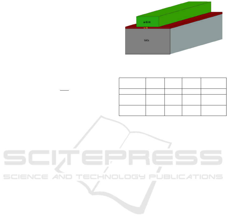
The structure under consideration is a rib waveguide
consisting of three different layers: SiO2 (cladding
layer), crystal silicon (c-Si) and a-Si:H (core layers),
as showed schematically in Fig. 1.
Figure 1: Schematic cross-section waveguide structure
Table 1: Layer geometries and physical parameters.
Height Width Length
Refractive
Index
Sio2 3 µm 3 µm 50 µm 1.44
Crystal
Silicon
220nm 3 µm 50 µm 3.47
amorphous
Silicon
h w 50 µm 3.57
Ansys Lumerical Photonic Multiphysics
Simulation tool (Bachorec & Sedlář, 2018) has been
used for numerical calculations, providing geometries
and physical material parameters for each layer
considered, as reported in Table 1. First, the
waveguide length was fixed to L=50 µm.
The optimal performance of semiconductor
devices is considered while determining the 220 nm
thickness of crystalline silicon (c-Si) in CMOS wafers
(Bellutti, Boscardin, Soncini, Zen, & Zorzi, 1995).
This thickness was chosen after thorough
consideration of all the factors of the optical device,
aiming to achieve optimal performance in both the
optical and electrical domains. The aim of this first
run of parametric simulations is to calculate the ideal
height (h) and width (w) for the a-Si:H layer to
achieve both criteria of SM behavior and PI.
4 SIMULATION RESULT
4.1 Single-Mode Condition
Parametric simulations have been performed to
calculate the difference between the effective index
of the modes propagating into the a-Si:H waveguide
core and the refractive index of the thin layer of c-Si
(nc-Si = 3.47). Fig. 2 shows the corresponding results,
at the wavelength of 1.55 µm, as a function of the a-
Si:H height. If a waveguide width of W=1.5 µm is
considered, the SM condition can be achieved for an
a-Si:H height ranging from 0.8 µm up to 2 µm.
Beyond these values, high-order modes appear.
Design and Simulation of Single-Mode and Polarization Independent Deeply Etched Amorphous Silicon on SOI Waveguides
95
Figure 2: Effective refractive index difference between the waveguide-core propagating optical modes and refractive index
of the c-Si as a function of the amorphous silicon height.
4.2 Polarization Independent (PI)
Waveguide
In Fig. 3, the effective refractive index of the
fundamental TE-polarized optical field is subtracted
from the effective index of the fundamental TM mode
as a function of the a-Si:H height, always considering
a constant value for the a-Si:H width (W = 1.5 µm) at
the wavelength of 1550 nm.
The a-Si:H height (h) that results in Δn equal to
zero is determined to be 1.22 µm about.
Figure 3: Difference between the effective refractive index
of TE and TM modes (Δn) as a function of the amorphous
silicon height.
4.3 Polarization Independent and
Single Mode Waveguide
To achieve both PI and SM conditions for different
cross-section waveguide geometries, parametric
simulations were performed for all of the
combinations of height (h) and width (w) of a-Si:H at
a fixed wavelength, as shown in Fig. 4. The achieved
results were used to identify the overlapping region
that meets both criteria.
Figure 4: a-Si:H height as a function of width. Both PI and
SM conditions are achieved in the range 1.4 µm<Wa-
Si:H<2 µm at the wavelength of 1.6 µm.
In order to extend the operating wavelengths beyond
the fiber-optic window, parametric simulations were
performed for wavelengths ranging from λ= 1.2 µm
to 1.6 µm. Fig. 5 shows heights and widths of a-Si:H
that simultaneously satisfy both PI and SM
conditions. It is worth noting that if the width of a-
Si:H is W=1.46 µm and the a-Si:H height falls in
between 1.19 µm and 1.15 µm, a SM and PI
waveguide can be achieved throughout the
considered wide wavelength window. The outcomes
of this study not only offer valuable insights into the
optimal geometric parameters of a-Si:H waveguides
for specific operational conditions but also provide a
pathway for enhancing their versatility across A
wider range of wavelengths. These findings
contribute to the ongoing efforts to advance the
development of efficient and adaptable photonic
devices for diverse applications in optical
communication and beyond.
PHOTOPTICS 2024 - 12th International Conference on Photonics, Optics and Laser Technology
96
(a)
(b)
Figure 5: a-Si:H height (h) as a function of width for different wavelengths (a), in the range 0.9 µm<Wa-Si:H<2 µm (b) in
the range 1.35 µm<Wa-Si:H<1.5 µm.
(a) (b) (c)
Figure 6: e-Field amplitude at the input (a), along the propagation direction (b) and at the waveguide output (c) for the PI and
SM waveguide 3 mm-length at λ= 1.5 µm.
4.4 Waveguide with Longer Length
In Fig. 6, finite-difference time-domain (FDTD)-
based simulation results about the propagation of the
fundamental TE/TM mode along a SM and PI
waveguide, L=3 mm long, are reported at various
positions along the propagation direction.
Based on Figure 6, despite a substantial increase
in the waveguide length, the guided mode
propagating through it shows no significant losses.
Consequently, it is reasonable to assume that the
simulated single-mode (SM) and polarization-
independent (PI) waveguide, characterized by a large
cross-sectional area, can be efficiently applied in the
development of both passive and active devices even
with extended length.
5 CONCLUSION
In this study, the design of single-mode and
polarization-independent large cross-section
waveguides have been investigated using commercial
software. We successfully identified the optimal
geometries to achieve both conditions in a wide
operating wavelength range, from 1.2 up to 1.6 um.
Design and Simulation of Single-Mode and Polarization Independent Deeply Etched Amorphous Silicon on SOI Waveguides
97

These results provide valuable insights to support the
ongoing advancement of optical communications by
developing new integrated electro-optic integrated
devices to be explored in many application fields,
from sensing to telecommunications.
ACKNOWLEDGMENT
Graphics project (F5) under the RESTART research
program (PE-14) (MUR PE00000001) is
acknowledged.
REFERENCES
Aalto, T., Cherchi, M., Harjanne, M., Bhat, S., Heimala, P.,
Sun, F., . . . Vehmas, T. (2019). Open-access 3-μm SOI
waveguide platform for dense photonic integrated
circuits. IEEE Journal of selected topics in quantum
electronics, 25(5), 1-9.
Bachorec, T., & Sedlář, T. (2018). A new era in simulation.
IEEE. Mikulov, Czech Republic.
Bellutti, P., Boscardin, M., Soncini, G., Zen, M., & Zorzi,
N. (1995). On the choice of the optimum silicon
substrate for CCD/CMOS technology. In Proceedings
of 4th International Conference on Solid-State and IC
Technology, 176-178.
Butt, M., & Kozlova, E. (2017). Single mode ZnO/Al2O3
Strip loaded waveguide at 633 nm visible wavelength.
Information technology and nanotechnology.
Dai, D., Liu, L., Gao, S., Xu, D.‐X., & He, S. (2013).
Polarization management for silicon photonic
integrated circuits. Laser & Photonics Reviews, 7(3),
303-328.
Della Corte, F. G., & Rao, S. (2013). Use of Amorphous
Silicon for Active Photonic Devices. IEEE
Transactions on Electron Devices, 1495-1505.
Jia-Ming, L. (2009). Photonic devices. Cambridge
University Press.
Lim, S., Eng Png, C., Ong, E., & Ang, Y. (2007). Single
mode, polarization-independent submicron silicon
waveguides based on geometrical adjustments. Optics
Express, 15(18), 11061-11072.
Ma, Y., Li, J., Han, Z., Maeda, H., & Pištora, J. (2021). All-
dielectric graphene-induced T-slot waveguide electro-
optic modulator with polarization-independent
operation. IEEE Journal of Selected Topics in Quantum
Electronics, 27(3), 1-8.
Marpaung, D., Yao, J., & Capmany, J. (2019). Integrated
microwave photonics. Nature photonics, 13(2), 80-90.
Neslihan, E., & Kurt, H. (2016). Model analysis of ridge
and rib types of silicon waveguides with void
compositions. IEEE Journal of Quantum Electronics,
52(10), 1-7.
Samanta, S., Dey, P. K., Banerji, P., & Ganguly, P. (2018).
A 1 × 2 polarization-independent power splitter using
three-coupled silicon rib waveguides. Journal of
Optics, 20(9), 095801.
Seong P., C., Eng Png, C., & Lim, S. (2004). polarisation
independent waveguides in silicon-on-insulator. Ist
IEEE International Conference on Group Iv Photonics,
115-117.
Spear, W., & Le Comber, P. (1975). Substitutional doping
of amorphous silicon. Solid state communications,
17(9), 1193-1196.
Zhang, L., Pan, C., Zeng, D., Yang, Y., Yang, Y., & Junxian
, M. (2020). A Hybrid-Plasmonic-Waveguide-Based
Polarization-Independent Directional Coupler. IEEE
Access , 8, 134268-134275.
PHOTOPTICS 2024 - 12th International Conference on Photonics, Optics and Laser Technology
98
