
Improving a Compressively Strained Ga
x
In
1-X
N
y
As
1-Y
/GaAs Multiple
Quantum Well Lasers for Emitting around 1300 Nm
F. Hadjaj, M. Belhadj, A. Nasri, I. Benyahia and K. Laoufi
Laboratory of Semiconductor Devices Physics, University of Bechar, P.O. Box 417, Bechar 08000, Algeria
Keywords: Multiple Quantum Well Laser, Nitrogen Incorporation, Ga
x
In
1-x
N
y
As
1-y
/GaAs.
Abstract: The objective of this work is to study the effect of Nitrogen incorporation on the structural and optical
properties of Ga
x
In
1-x
N
y
As
1-y
semiconductor alloy in order to obtain quantum well Ga
x
In
1-x
N
y
As
1-y
/GaAs
structures emitting at wavelengths around 1.3 μm. We also investigated their effect on the band gap energy,
the electron effective mass, the optical gain, and the optical confinement. The incorporation of Nitrogen in
the Ga
x
In
1-x
As alloy gave very particular and attractive properties, the most important being the reduction of
the band-gap energy and a significant increase in effective mass, which results in an increase in the emission
wavelength. The anticrossing band model describes these properties. It is also found that the optical gain
and confinement factor were found to be strongly increased when the Nitrogen content was reduced. In
order to achieve a wavelength of 1.3 μm and maintain a high-quality structure, we found that decreasing the
Gallium composition (x) and increasing the Nitrogen composition (y) simultaneously gave accurate results.
1 INTRODUCTION
The GaInNAs/GaAs quantum-well system has
attracted much interest over the past 10 years due to
its advantages over conventional III-V alloys. The
reduction of the band gap of GaInNAs and its lattice
matching to GaAs allow for optoelectronic devices
based on a GaAs substrate, which emits in the
optical fibre windows of 1.3 and 1.55 µm (Qiu,
2008). Long-wavelength 1.3 and 1.55 µm
optoelectronic devices such as lasers, detectors,
filters, and optical amplifiers are key components of
present optical fibre communications because of the
minimum loss in this wavelength region (Fang,
2006). So far, many high-efficiency GaInNAs-based
lasers have been reported. However, the physics of
GaInNAs is still not fully understood and has been
under intensive study for the last few years.
Different approaches, such as the band-anticrossing
model, empirical pseudo-potential super cell
method, first principles pseudo-potential method,
and tight-binding method, were proposed in order to
explain the GaInNAs band structure and its optical
properties (Kudrawiec, 2004). A major breakthrough
was achieved for dilute nitride alloys with the
demonstration by Walukiewicz and co-workers that
the reduction in energy gap in Ga(In)N
x
As
1−x
is due
to a band-anticrossing interaction between the
conduction band edge and higher-lying localised
nitrogen resonant states (Shan, 1999).. Given the
significant differences in the conduction band
structure of GaInNAs compared to conventional III-
V semiconductors, it is important to elucidate the
influence of N not only on the electronic structure
but also on the gain characteristics of ideal dilute
nitride lasers (Broderick, 2012). In the present paper,
our study has focused on the improvement of Ga
x
In
1-
x
As
y
N
1-y
/GaAs multiple quantum well lasers
operating continuously for longer wavelengths with
the incorporation of Nitrogen, and this by optimising
the important parameters of the laser, which are the
optical gain and the confinement factor. To this
purpose, we carried out a detailed study of all the
properties of the quantum well system based on
Ga
x
In
1-x
As
y
N
1-y
/GaAs. We began with band gap
energy and electron effective mass using the band-
anticrossing (BAC) model, then determined the
optical gain and confinement of the Ga
x
In
1-x
As
y
N
1-
y
/GaAs heterostructure.
2 THEORY AND MATERIAL
PARAMETERS
The lasers used in this study are multiple quantum
well lasers.Our suggested structure comprises a QW
Hadjaj, F., Belhadj, M., Nasri, A., Benyahia, I. and Laoufi, K.
Improving a Compressively Strained Ga x In 1-X N y As 1-Y /GaAs Multiple Quantum Well Lasers for Emitting around 1300 Nm.
DOI: 10.5220/0012324900003651
Paper published under CC license (CC BY-NC-ND 4.0)
In Proceedings of the 12th International Conference on Photonics, Optics and Laser Technology (PHOTOPTICS 2024), pages 39-44
ISBN: 978-989-758-686-6; ISSN: 2184-4364
Proceedings Copyright © 2024 by SCITEPRESS – Science and Technology Publications, Lda.
39
layer of Ga
0.7
In
0.3
N
y
As
1-y
material having a thickness
of 7 nm placed between two wide band gap barrier
layers of GaAs material having a thickness of 10
nm, followed by cladding layers of Al
0.4
Ga
0.6
As
material of 2 µm thickness. Clearly, the quantum
well layer band gap is narrower as compared to that
of the barrier region, and the barrier layer band gap
is narrower as compared to that of the cladding
region. Our structure has the same thickness and the
same Gallium composition; the composition of
Nitrogen is the only parameter that can be varied, as
its value changes from 0 to 4%. The compositions of
Ga
0.7
In
0.3
N
y
As
1-y
alloys (well) suitable for long-
wavelength lasers grown on GaAs alloy (barrier) are
selected arbitrary, taking into account the built-in
strain in the well material and a desired emission
wavelength. We assumed that for 7 nm-wide QW
grown on GaAs, the compressive strain should be ≤
2%. The content of Gallium (x) is kept constant;
only the Nitrogen content (y) is added to the well
material. We found that it leads to a small reduction
of the compressive strain in the QW. We also found
that the lattice mismatch defined by the parameter
(ε) is negative, whatever the value of the N
concentrations. This means that our Ga
0.7
In
0.3
N
y
As
1-
y
/GaAs heterostructure is under compression. The
choice of the alloy composition adopted in our study
(y from 0 to 4%) is due to the low mesh mismatch (ε
≤ 2%) between the well and the barrier for these
compositions and the wavelength to be obtained.
Our Ga
0.7
In
0.3
N
0.01
As
0.99
/GaAs hetero-structure is
characterised by a weak bi-axial compressive strain
of the order ε = Δa/a = -1.9%, while the
Ga
0.7
In
0.2
N
0.02
As
0.98
/GaAs hetero-structure has a bi-
axial compressive strain of the order ε = -1.7%
(Hadjaj, 2021). In order to improve the performance
of Ga
0.7
In
0.3
N
y
As
1-y
/GaAs quantum well lasers, the
Nitrogen composition of the Ga
0.7
In
0.3
N
y
As
1-y
well
should be reduced, although this leads to increased
strain in the quantum wells. The Ga
x
In
1-x
N
y
As
1-y
alloy is a material that combines binary compounds
such as GaAs, InAs, GaN, and InAs to crystallise in
the zinc-blend structure. The parameters of the four
binaries are as illustrated in Table 1.
Table 1: Basic properties of the binary semiconductors
GaAs, InAs, GaN, and InN in the zinc-blende structure
used for the computations: Eg, energy gap; a
0
, lattice
constant; me/m0, electron effective mass; α and 𝛃,
Varshni’s parameters; and n, refractive index calculated by
Herve and Vandamme relation (H.V.). Our calculated
results were compared with the available theoretical and
published values and showed excellent agreement (Ioffe,
2013).
Paramete
r
GaAs InAs GaN InN
𝐸
(0 K )
(eV)
𝐸
(300 K )
(eV)
α(Γ)
(10
-4
eV/K)
𝛃(Γ) (K)
a0 (Å )
m
e
/m
0
n
(theoretical)
n (calculated
by H.V)
1.519
a,b
1.422
d
5.405
b
204
b
5.6533
b
0.067
b
3.3
c
2.99
d
0.417
a,b
0.354
d
2.76
b
93
b
6.0584
b
0.023
c
3.51
c
3.758
d
3.299
b
3.24
d
5.93
b
600
b
4.50
b
0.15
b
2.3
c
2.208
d
1.94
b
1.916
d
2.45
b
624
b
4.98
b
0.12
b
2.9
c
3.404
d
a
Ref. (Fox, 2010),
b
Ref. (Vurgaftman, 2003),
c
Ref. (Ioffe,
2013),
d
Ref. calculated.
The refractive indices for the ternaries and for
the quaternaries are then calculated from the indices
of the binaries according to Vegard's laws (Takagi,
1982).The refractive index of ternary
alloys 𝐴
𝐵
𝐶 and 𝐴𝐵
𝐶
are usually given as:
𝑛
𝑥𝑛
1𝑥
𝑛
(1)
𝑛
𝑥𝑛
1𝑥
𝑛
(2)
And it expression for quaternary A
x
B
1-x
C
y
D
1-y
is
given by the following relation:
𝑛
𝑦
1𝑥
𝑛
1𝑥
1𝑦
𝑛
𝑥𝑦𝑛
𝑥
1𝑦
𝑛
(3)
The variation of refractive index is also
calculated using empirical Herve and Vandamme’s
formula, which is a function of band gap energy:
𝑛
1
(4)
Where A and B have the values 6.13 and 3.4 eV,
respectively. In fact, the semiconductor refractive
index is a fundamental physical parameter that
characterises optical and electrical properties
(Koezuka, 1987).
PHOTOPTICS 2024 - 12th International Conference on Photonics, Optics and Laser Technology
40
3 BAND ANTI-CROSSING
MODEL
Many models were proposed for the calculation of
the band gap energy of GaInNAs alloys, and the
most accepted theory is that of the band-anticrossing
(BAC) model. Low concentrations of N introduce a
highly localised acceptor-like level in conventional
Ill-V semiconductors. This narrow resonant band
interacts strongly with the conduction band,
ultimately leading to the splitting of the conduction
band and a reduction of the fundamental energy
band gap. The two resulting coupled bands
areidentified as E- and E+, and a simple model of
two interacting energy levels can be used to find
their dispersion relationship.
𝐸
𝑘
12
⁄
𝐸
𝑘
𝐸
𝐸
𝑘
𝐸
4𝑦𝑉
(5)
Where E
M
(k) is the conduction band energy of
InGaAs, E
N
is the energy of the N level relative to
the top of the valence band, and V
MN
is the matrix
element describing the interaction between E+ and
E- (Shan, 1999, Skierbiszewski, 2002). The
functional form for V
MN
and E
N
parameters reads :
𝑉
𝐶
𝑦
with 𝐶
2.7 for 𝑥0.93 (6)
In the above, y is the Nitrogen concentration,
and C
MN
is the parameter that depends on the matrix
semiconductor, hence the In composition (Erol,
2008,Sze, 1981). Based on this BAC model, the
shifting-down energy gap is given by (Yu, 2001):
∆𝐸
𝐸
𝐸
4𝑦𝑉
𝐸
𝐸
2
⁄
(7)
In semiconductors, the effective mass
approximation only works for the parabolic energy
dispersion at small wave vectors k and for small
electron energies close to the minimal Γ point.
However, due to N incorporation, the conduction
band energy saturates at relatively low k magnitude,
resulting in a heavy effective electron mass at higher
energy levels in the GaInNAs alloys. To include the
non-parabolic conduction band, the approach
developed by Zawadzki is used. It calculates non-
parabolic dispersion in small-band gap
semiconductors (Zawadzki, 1974). Energy affects
the electron effective mass 𝑚
, and its inverse is as
follows:
.
(8)
Replacing E(k) by equation 5, the analytic
expression for k-dependent inverse electron effective
masses of Nitrogen-containing alloys is:
.
.1
.
(9)
Where 𝑚
𝑘
is the electron effective mass of
the host material, such as Ga
x
ln
1-x
As in the case of
Ga
x
ln
1-x
N
y
As
1-y
(Skierbiszewski, 2000).
4 RESULTS AND DISCUSSION
First, we study the band properties of the Ga
x
ln
1-
x
N
y
As
1-y
alloy. We start by determining the variation
of the band gap energy as a function of the Nitrogen
composition (y≤4%) for different Gallium
compositions.
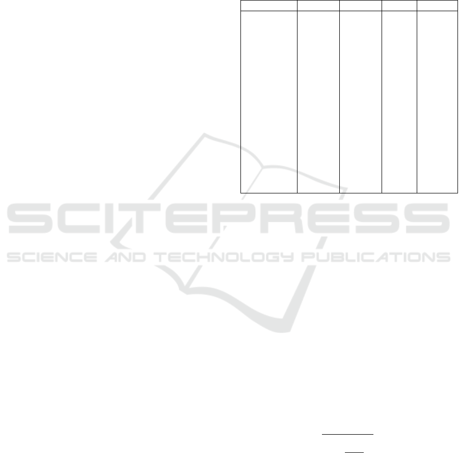
Figure 1: (a) The band gap energy and (b) the shifting
down energy gap as a function of Nitrogen composition
(y), for different compositions of Gallium (x) in Ga
x
In
1-
x
As
1-y
N
y
alloys, the band gap is calculated using Vegard’s
law.
It can be seen that if the concentration of
Nitrogen increases, the energy of the band gap
decreases, if we set the concentration of Ga (x) at
0.7, the band gap of the Ga
0.7
In
0.3
As
1-y
N
y
alloys as a
function of the Nitrogen concentration y decreases
with the increase in the proportion of Nitrogen y and
it increases with increase in the proportion of
Gallium x, Furthermore, the addition of N decreases
0,00 0,01 0,02 0,03 0,04
0,5
0,6
0,7
0,8
0,9
1,0
1,1
1,2
1,3
Band gap energy,eV
Nitrogen content,y
Ga = 70 %
Ga = 80 %
Ga = 90 %
Linear fit
0,00 0,01 0,02 0,03 0,04
-0,05
0,00
0,05
0,10
0,15
0,20
0,25
0,30
0,35
Shifting down energy gap,eV
Nitrogen content,y
BAC Model
E
g
Ga
0.7
In
0.3
N
y
As
1-y
C
MN
= 2.7 eV
Δ
(a)
(b)
Improving a Compressively Strained Ga x In 1-X N y As 1-Y /GaAs Multiple Quantum Well Lasers for Emitting around 1300 Nm
41
the band gap energy of Ga
x
In
1-x
As
1-y
N
y
material
system, thus rapidly reaching the long wavelength
emission region. Figure 1 shows also the variation of
the shifting down energy gap as a function of
Nitrogen composition (y) in Ga
0.7
In
0.3
As
1-y
N
y
alloys.We found that when the Nitrogen
concentration becomes important (4%), ΔEg reaches
0.338 eV. From this we conclude that the shifting
down energy gap is increased with an increase in
Nitrogen content in Ga
0.7
In
0.3
As
1-y
N
y
alloys.
Figure 2: (a) The band gap energy and (b) the electron
effective mass as a function of Nitrogen composition (y),
the curves are calculated using the band-anticrossing
model.
We see that at a certain percentage of Nitrogen, the
band gap splits into two bands, and the more the
Nitrogen concentration increases, the more this split
becomes important. These results are very close to
the theoretical results of Refs (Aissat, 2007,
Spruytte, 2001, Yasar, 2015). The band anti-crossing
(BAC) model can explain this significant reduction
of the band gap with Nitrogen incorporation.
Nitrogen atoms are smaller and have a higher
electronegativity than as atoms, which leads to the
formation of defect states near the edge of the
conduction band. These Nitrogen-related defects are
highly localised and form a narrow band that
resonates with the extended states of the GaInAs
conduction band. This coupling through anticrossing
interaction results in the splitting of the conduction
band into two subbands. Figure 2 shows also the
variation of the electron effective mass m
e
*
for
Ga
x
In
1-x
As
1-y
N
y
alloy with different Gallium and
nitrogen contents. As can be seen, a very large
increase of the effective mass is found with higher N
composition, the reduced band gap energy by adding
N increases the electron effective mass, which it is
in good qualitative agreement with the predictions of
the BAC model.
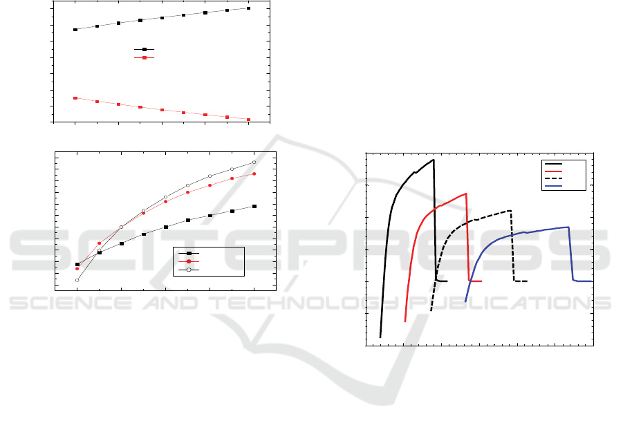
The optical gain In a semiconducto” las’r Is an
essential parameter to characterise fabricated lasers
and to simulate their behavior. Figure 3 represents
the variations of the optical gain as a function of the
wavelength for different values of the Nitrogen
composition. In order to obtain a structure with an
emission wavelength of 1.3 µm, we decreased the
Gallium composition, fixed it at 0.7, and increased
the Nitrogen composition from 1% to 4% to reduce
strain, as we had previously found that increasing
Nitrogen decreases strain. Then we determined the
best structure that gave us the desired emission
wavelength.
Figure 3: TE mode of the optical gain as function of
wavelength for Ga
0.7
In
0.3
N
y
As
1-y
/GaAs SQWs for different
compositions of Nitrogen (y) obtained for the well with 7
nm, a barrier of 10 nm, an intraband relaxation time of 0.5
ps, and an ambient temperature of 300 k.
It Is noted that Increasing the carrier density In
the active region causes an increase in the maximum
optical gain. This phenomenon is linked to the filling
of the high states of the conduction and valence
bands with an increase in the number of carriers. We
easily observed that varying the N composition
shifts the optical gain spectrum towards longer
wavelengths and reduces the maximum optical gain,
as shown in figure 3. The shift in the gain spectrum
is due to the decrease in the gap of Ga
0.7
In
0.3
N
y
As
1-y
while the decrease in the maximum optical gain is
particularly due to the reduction in optical
confinement since the refractive index is higher in
0,00 0,01 0,02 0,03 0,04
0,8
1,0
1,2
1,4
1,6
1,8
2,0
2,2
Band gap energy,eV
Nitrogen content,y
Eg
+
Eg
-
Ga
0.7
In
0.3
N
y
As
1-y
C
MN
= 2.7 eV
0,00 0,01 0,02 0,03 0,04
0,040
0,045
0,050
0,055
0,060
0,065
0,070
0,075
0,080
0,085
0,090
0,095
Electron effective mass
Nitrogen content,y
Ga = 70 %
Ga = 80 %
Ga = 90 %
0,8 1 1,2 1,4 1,6 1,8 2
-20 000
-10 000
0
10 000
20 000
30 000
40 000
max
=1.161
m
Wavelength,µm
Optical gain TE mode, m
-1
max
=1.332
m
max
=1.567
m
max
=1.874
m
N = 1%
N = 2%
N = 3%
N = 4%
(a)
(b)
PHOTOPTICS 2024 - 12th International Conference on Photonics, Optics and Laser Technology
42
the active layer than in the adjacent layers for a high
concentration of Nitrogen. We conclude that the
gain spectrum shifts by varying the Nitrogen and
Gallium compositions. To reach high wavelengths,
we must decrease the Gallium composition and
increase the Nitrogen composition.
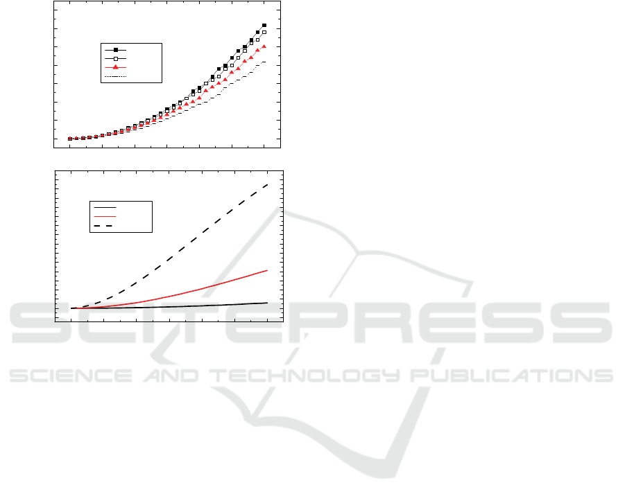
Figure 4: The confinement factor as a function of well
width (a) for different Nitrogen composition (y) (b) for
different well number.
Figure 4 displays how the confinement factor
changes with well width for a
Ga
0.7
In
0.3
N
0.02
As
0.98
/GaAs structure with different
numbers of wells. The number of wells multiplied
by the well width is a crucial component of the
structure that improves confinement factor. This
figure also represents the variation of the
confinement factor as a function of the well width
for different N compositions. It is observed that the
confinement factor increases with the increase in the
well width and decreases with the increase in the N
composition. We also see that the wavelength
increases by increasing the Nitrogen composition;
this increase is due to the decrease in the energy of
the band gap with the Nitrogen composition. To
reach a wavelength of 1.3 μm, we reduce the
composition of Gallium and increase the
concentration of Nitrogen from 1% to 4%, as well as
the width of the quantum well. To achieve the
desired wavelength, we must choose the right
compositions of the Material used for the wells to
obtain the corresponding band gap energies. We
must also choose the right compositions of the
material used for the barrier to have a good mesh
agreement or a mesh disagreement less than 2%. To
avoid carrier leakage, we must have good
confinement of electrons and holes. From this we
conclude that the incorporation of Nitrogen has led
to degradation in the structure’s properties, as we
noticed that adding a small percentage of Nitrogen
reduces both gain and confinement. It also reduces
the band gap, which increases the emission
wavelength, in addition to increasing the strain.
5 CONCLUSIONS
In conclusion, the effect of the incorporation of
Nitrogen on the properties of Ga
x
In
1-x
N
y
As
1-y
/GaAs
MQWs has been carried out. The band-anticrossing
model (BAC) is used to describe the band gap
energy and the effective mass when Nitrogen is
incorporated into the quaternary Ga
x
In
1-x
N
y
As
1-y
.
These properties are mostly degraded because a
small amount of Nitrogen (usually less than 5%) is
added to GaInAs to make GaInNAs alloys that emit
at 1.3 µm. We come to the conclusion that
increasing the Nitrogen ratio increases the emission
wavelength while also significantly increasing the
electron effective mass and decreasing the band gap
energy.The decrease in energy is due to the
interaction of the energy of the conduction band
with the level of Nitrogen, and moreover, as the
concentration of Nitrogen increases, the energy gap
of the band decreases.The interaction splits the
conduction band into two non-parabolic sub-bands
with energy-dependent effective masses. The
downward shift of the lower sub-band fully explains
the N-induced reduction of the energy gap. Our
results also show that increasing the proportion of
Nitrogen makes it possible to reach wavelengths that
can exceed 1.3 μm but causes a reduction in gain
and confinement factor. Finally, to make Ga
x
In
1-
x
N
y
As
1-y
/GaAs quantum well lasers work better, this
material needs to have an emission wavelength of
1.3 µm. To do this, it is important to look at how
Gallium and Nitrogen are mixed. The composition
of these two materials will give the appropriate
energy band gap, hence the desired emission
wavelength.
0 5 10 15 20 25 30
0,000
0,005
0,010
0,015
0,020
0,025
0,030
0,035
Confinement factor
Well width
(
nm
)
N = 1 %
N = 2 %
N = 3 %
N = 4 %
0 5 10 15 20 25 30
-0,05
0,00
0,05
0,10
0,15
0,20
0,25
0,30
0,35
0,40
0,45
0,50
0,55
0,60
0,65
0,70
0
,
75
Confinement factor
Well width (nm)
1 Well
3 Wells
5 Wells
(a)
(b)
Improving a Compressively Strained Ga x In 1-X N y As 1-Y /GaAs Multiple Quantum Well Lasers for Emitting around 1300 Nm
43

REFERENCES
Qiu,Y.N., Sun, H.D., Rorison, J.M., Calvez,S., Dawson,
M.D., Bryce, A.C.(2008).Quantum Well Intermixing
Influence on GaInNAs/GaAs Quantum Well Laser
Gain: Theoretical Study, Semiconductor Science and
Technology, 23 (9), 095010.
Fang,I.L.,Kuo,S.Y.,Wang,J.S.,Hsiao,R.S.,Kuo,H.C.,Chic,J
.,Wang,S.C.,Wang,H.S.,Liang,C.T.,Chen,Y.F.(2006).
Temperature-Dependent Optical Properties of
In
0,34
Ga
0,66
As
1-x
N
x
/GaAs Single Quantum Well With
High Nitrogen Content for 1:55 mm Application
Grown by Molecular Beam Epitaxy, Journal of Crystal
Growth 291,27–33.
Kudrawiec,R., Misiewicz, J., Pavelescu, E.-M., Konttinen,
J., Pessa, M.(2004). Metastability of Band-Gap Energy
in GaInNAs Compound Investigated by Photo-
reflectance, ActaPhysicaPolonica A, No. 2, Vol. 106.
Shan, W.,Walukiewicz, W., Ager Ill, J. W., HaIler, E. E.,
Geisz, J. F., Friedman, D. J.,Olson, J. M.,
Kurtz,S.R.(1999).Band Anticrossing in GalnNAs
Alloys,l'hys. Rev. Lett. 82, 1221.
Broderick, C. A., Usman, M., Sweeney.S.J., O’Reilly, E.P.
2012.Band engineering in Dilute Nitride and Bismide
Semiconductor Lasers, Semicond. Sci. Technol., vol.
27, p. 094011.
Hadjaj,F.,Belhadj,M.,LaoufI,K.,Missoum,A.(2021)
Optimized Design of Strain-Compensated In
X
Ga
1-
X
N/GaN and In
X
Ga
1-X
N/In
Y
Ga
1-Y
N Multiple-
Quantum-Well Laser Diodes, Journal of Ovonic
Research, Vol. 17, No. 2, p. 107 – 115.
Fox,M.(2010).Optical properties of solids,2
nd
edition.
Vurgaftman,I., Meyer,J.R.(2003).Journal of applied
physics 94, 3675.
NSM archive (2013).Physical properties of
semiconductors. Ioffe physical technical institute.
Takagi,T.,Yamakoshi,Y.,Yamaura,M.,Kondow,R.,Matsus
hima,T.(1982).Development of a New Type Fault
Locator Using the One-Terminal Voltage and Current
Data, The Tokyo Electric Power Con , Vol. 101, No 8,
pp 2892-2898.
Koezuka,H.,Tsumura,A.,Ando,T. (1987). Field-effec
Transistor WithPolythiophene Thin Film, Synthetic
Metals, Volume 18, Issues 1–3, 699–704.
Skierbiszewski,C. (2002). Experimental Studies of the
Conduction-Band Structure of GalnNAs
alloys,Semicond. Sci. Technol. 17,80.
Erol,A, (2008).Dilute III-V nitride semiconductors and
material systems: physics and technology. berlin:
springer.
Sze,S.M.(1981).Physics of Semiconductor Devices,
2
nd
Edition.
YuK, M.,Walukiewicz,W., Wu,J.,Beeman, J.W., Ager III,
J.W.,Haller,E.E.,Shan, W.,Xin, H.P.,Tu, C.W. (2001).
Applied Physics Letters 90.
Zawadzki,W. 1974. Electron Transport Phenomena in
Small Gap Semiconductors, Adv. Phys. Vol. 23, pp.
435-522.
Skierbiszewski,C.,Perlin,P.,Wisniewski,P.,Knap,W.,Suski,
T. (2000). Appl. Phys. Lett., vol.76, Number 1.
Aissat,A.,Nacer,S., El-Bey,M.,Guessoum,A.,Ferdjani,K.,
Berkani,D.,Vilcot,J.P. (2007).The Effect of Nitrogen
on the Energy Gap of a Structure with Strained
Quantum Well Containing GaInNAs/GaAs, Iranian
Journal of Electrical and Computer Engineering, Vol.
6, No. 2, summer-fall.
Spruytte,S.G.,Larson,M. C., Wampler,W.,Coldren,C.
W.,Petersen,H.E.,Harris,J.S.(2001).Nitrogen
Incorporation In Group III-Nitride-Arsenide Materials
Grown by Elemental Source Molecular Beam Epitaxy,
J. Cryst. Growth, Vol. 227, No. 28, pp.506-515.
Yasar,S.,Bilican,I.,Oduncuoglu,M.,Agan,S.,Uluer,I.(2015)
.Optical Properties of In
x
Ga
1-x
N
y
As
1-y
/GaAs
Heterostructure Quantum Well Lasers for 1.3 µm
Laser Emission with Different In/N Concentrations,
International Journal of Scientific and Technological
Research ,ISSN 2422-8702 , Vol 1, No.1.
PHOTOPTICS 2024 - 12th International Conference on Photonics, Optics and Laser Technology
44
