
Barrier Structure for Ga-Free Type-II Superlattice Midwave
Infrared Photodetector
P. Christol
1
, M. Bouschet
1,2
, J. P. Perez
1
and N. Péré-Laperne
2
1
IES, Univ. Montpellier, CNRS, Montpellier, France
2
LYNRED, BP 21, Veurey-Voroize, France
Keywords: Midwave Infrared Photodetector, Barrier Structure, Ga-Free Type-II Superlattice.
Abstract: This paper reports on electrical and electro-optical characterizations of Ga-free InAs/InAsSb type-II
superlattices (T2SL) midwave infrared barrier photodetectors grown by Molecular Beam Epitaxy on GaSb
substrate. Experimental measurements are made of photo-response and dark current density-voltage (J-V)
measurements performed as a function of temperature and transport of minority carrier in this barrier
detector is discussed. Results obtained at 150 K for 5µm cut-off wavelength are at the state of the art but
identification of an high bias voltage operation demonstrates that the barrier layer has to be improved.
1 INTRODUCTION
High performance cooled photodetectors operating
in the midwave infrared (MWIR, 3-5µm)
atmospheric spectral window are used in a wide
variety of applications in imaging and sensing. To
keep high signal to noise ratio, it is necessary to
reduce the operating temperature of the IR detector
system to cryogenic temperatures, which involves
the implementation of a cryocooler inducing
significant restrictions in term of weight,
compactness and energy autonomy. Mitigating these
constraints is essential to generate new class of
applications using, for example, handheld thermal
imagers or embedded systems on unmanned aerial
vehicles. Consequently, enhancing the temperature
operation, without penalizing performance of
detectors, is currently one of the main challenges
investigated by the IR detector community.
InSb (Indium Antimonide) and MCT (Mercury
Cadmium Telluride) cooled photodetectors are the
currently dominant technologies in the MWIR
domain. However, despite high performances
reached, such commercial technologies have some
limits : InSb suffers from a low Shockley-Read-Hall
lifetime, close to 700 ns, limiting its operating
temperature at 80-90K ; MCT can operate at
temperature as high as 110-120K for 5µm cut-off
but is very challenging to manufacture and a few
number of providers can handle it. Consequently,
there is a need to develop an new MWIR technology
with high temperature operation (T = 150 K) and
strain-balanced Ga-free InAs/InAsSb Type-II
superlattice (T2SL) on GaSb substrate, especially
combined with a barrier structure design, seems
promising to address some of these limitations.
Since the work reported by Maimon and Wicks
(Maimon and Wicks, 2006) on InAs detector, barrier
structure also called XBn (Klipstein, 2011), is now
the usual design of high performance MWIR
photodetector. In a barrier structure, a large band
gap material, namely the barrier layer (BL), is
inserted after the absorption layer (AL) to block the
majority carriers while allowing unimpeded
transport of the minority carriers to the contact layer
(CL). The electric field being confined in the BL, the
generation-recombination (G-R) current is
suppressed in the absorption region and the dark-
current of such a structure, when properly designed,
is thus diffusion-limited whatever the temperature.
The electrical performances of XBn devices are
therefore improved compared to the usual pin
photodiodes and temperature operation as high as
150 K is reached for the MWIR (Ting, 2018), but
many works have still to be done to improve their
electrical and electro-optical performances.
This paper reports on design, fabrication and
characterization of Ga-free InAs/InAsSb T2SL
MWIR photodetector, grown by molecular beam
epitaxy (MBE) on GaSb substrate.
Christol, P., Bouschet, M., Perez, J. and Péré-Laperne, N.
Barrier Structure for Ga-Free Type-II Superlattice Midwave Infrared Photodetector.
DOI: 10.5220/0011624500003408
In Proceedings of the 11th International Conference on Photonics, Optics and Laser Technology (PHOTOPTICS 2023), pages 21-27
ISBN: 978-989-758-632-3; ISSN: 2184-4364
Copyright
c
2023 by SCITEPRESS – Science and Technology Publications, Lda. Under CC license (CC BY-NC-ND 4.0)
21
2 DESIGN OF THE GA-FREE
INAS/INASSB SUPERLATTICE
BARIER STRUCTURE
The three semiconductor materials InAs, GaSb, and
AlSb form an approximately lattice-matched set
around 6.1 A, covering a wide range of band-gap
energies (Figure 1).
5.6 5.8 6.0 6.2 6.4 6.6
0.0
0.5
1.0
1.5
2.0
°
Lattice parameter (A)
T2SL AL
AlAs
0.09
Sb
0.91
BL
InP
Energy (eV)
InAs
InSb
GaSb
AlSb
GaAs
AlAs
InAs
1-x
Sb
x
Figure 1: Band-gap energy as a function of lattice
parameter of common III-V semiconductor materials. The
dashed line shows the lattice parameter of GaSb
compound near 6.1 A.
Considering a GaSb substrate, Ga-free InAs/InAs
1-
x
Sb
x
T2SLs can be strain-balanced on GaSb by
choosing appropriate combinations of layer
thicknesses and InAs
1-x
Sb
x
alloy compositions.
Typically, the tensile strain in InAs is compensated
by the compressive strain introduced in InAs
1-x
Sb
x
leading to a thicker InAs layer compared to the
InAsSb one. Precisely, strain balancing is achieved
by setting the average lattice parameter of one
period of the SL equal to the lattice parameter of
GaSb. Consequently, the InAsSb and InAs layer
thicknesses (t
InAsSb
and t
InAs
, respectively) as a
function of the Sb composition (x
Sb
) and T2SL
period (P) can be calculated by using the equations :
𝑡
=
𝑎
−𝑎
𝑎
−𝑎
.
𝑃
𝑥
= 0.090 .
𝑃
𝑥
(1)
𝑡
+𝑡
=𝑃
with a
GaSb
=6.0954 Å ; a
InAs
= 6.0584 Å ;
a
InSb
=6.4794 Å, the lattice parameters of the binary
compounds.
Figure 2 shows the evolutions of t
InAsSb
and t
InAs
as a functions of antimony concentration (x
Sb
) for a
6nm period thick of strain-balanced InAs/InA
1-x
Sb
x
T2SL. For a given x
Sb
value, one can extract the
thicknesses of each SL layer.
0.10.20.30.40.50.60.70.80.91.0
0
2
4
6
8
10
12
14
16
18
20
t
InAsSb
number of monolayers (MLs)
Antimony concentration x
Sb
InAs/InAs
1-x
Sb
x
T2SL with P = 6 nm (19.73 MLs)
t
InAs
Figure 2: Calculated InAs and InAsSb thicknesses as
functions of x
Sb
for a 6nm (19.73 monolayer (MLs))
period of strain-balanced InAs/InAsSb T2SL on GaSb
substrate. Considering an InAs/InAs
0.65
Sb
0.35
SL structure,
strain-balanced condition is obtained for t
InAs
= 14.7 MLs
and t
InAsSb
= 5 MLs.
The quantized miniband energies of the strain
balanced InAs/InAs
1-x
Sb
x
T2SL, for different
antimony concentrations x
Sb
and SL period, were
calculated using the k p formalism and the envelope
function approximation available in the Nextnano3
commercial software.
A type II-b InAs/InAsSb heterostructure band
offset, with electrons confined in the InAs layer and
holes confined in the InAsSb one, has been taken
into account (Lakner, 2012 ; Steenbergen, 2012).
Due to this band alignment, inducing a spatial
indirect valence to conduction energetic transition,
the absorption coefficient of the InAs/InAsSb T2SL
has a strong dependence on the electron-hole
wavefunction overlap |<Φ
C
|Φ
V
>|
2
which is governed
by the x
Sb
composition and period thickness of the
strain-balanced SL (Webster, 2015).
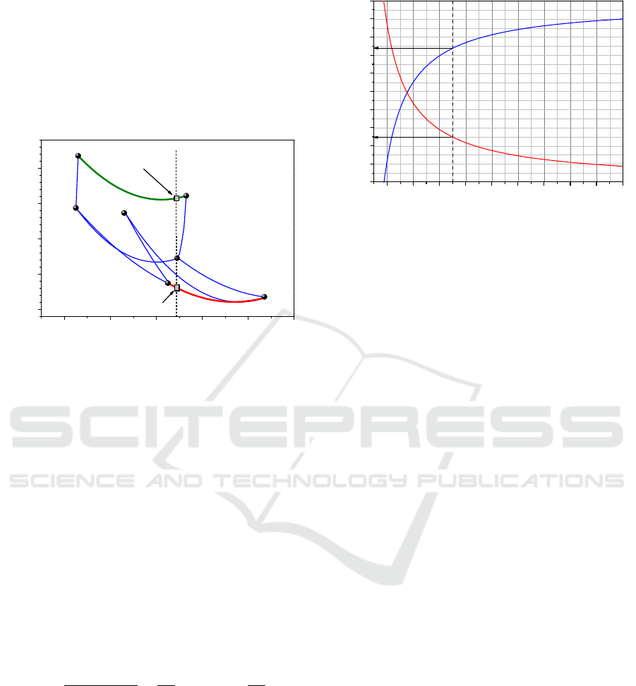
Results in terms of cut-off wavelength of
expected Ga-free MWIR T2SL detector system
corresponding to the ground heavy hole VH1 to
conduction C1 interminiband absorption, are plotted
on Figure 3. Calculations were made at T = 150K for
x
Sb
composition varying from 0.25 to 0.4 and T2SL
period (P) varying from 4 nm to 8 nm. |<Φ
C1
|Φ
VH1
>|
2
wavefunction overlap values calculated for each
fundamental VH1-C1 transition are specified. We
can note that the wavefunction overlap can be
increased by shortening the period of the superlattice
for a given Sb concentration, or decreasing the Sb
concentration for a given period P.
In order to reach the full MWIR spectral band
with cut-off wavelength equal to 5µm,
InAs/InAs
1-x
Sb
x
SL structure with Sb content
PHOTOPTICS 2023 - 11th International Conference on Photonics, Optics and Laser Technology
22
x
Sb
= 0.35 and SL period p = 6nm made of
t
InAs
=4.5 nm (14.7 MLs) and t
InAs
=1.5 nm (5MLs)
could be of interest since this T2SL exhibits cut-off
wavelength higher than 5 µm at 150K for a
wavefunction overlap higher than 50% (Figure 3).
0.24 0.26 0.28 0.30 0.32 0.34 0.36 0.38 0.40 0.42
4.0
4.2
4.4
4.6
4.8
5.0
5.2
5.4
5.6
5.8
6.0
6.2
6.4
6.6
6.8
7.0
37.3%
40.8%
45.4%
51.6%
51.4%
55%
59.3%
63.2%
65.1%
66.2%
70%
75%
78.1%
80.3%
82.7%
p=8nm
p=6nm
p=5nm
p=4nm
calculated cut-off wavelength λ
VH1-C1
(µm)
Antimony concentration x
Sb
InAs/InAs
1-x
Sb
x
T2SL
T = 150 K
85.8%
Figure 3: Strain balanced InAs/InAs
1-x
Sb
x
T2SL on GaSb
substrate: Calculated cut-off wavelength at T = 150K and
associated wavefunction overlap of the ground VH1-C1
miniband transition as a function of Sb concentration (x
Sb
)
and for different period thicknesses (P).
Figure 4 displays the schematic band diagram of
the chosen InAs(4.5nm)/InAs
0.65
Sb
0.35
(1.5nm) T2SL
structure at T= 150K, showing a fundamental
|<Φ
C1
|Φ
VH1
>|
2
wavefunction overlap equal to 55%.
InAs/InAs
0.65
Sb
0.35
T2SL
InAsSb
InAs
φ
2
C1
VL1 light hole
miniband
VH1 heavy hole
miniband
C1 electron
miniband
φ
2
VH1
I<
φ
C1
I
φ
VH1
>I
2
= 55%
Figure 4: Schematic band diagram of the Ga-free
InAs/InAs
0.65
Sb
0.35
T2SL structure. On the lower part,
fundamental electron (C1) and heavy hole (VH1) presence
probability densities are reported, showing a wavefunction
overlap equal to 55%.
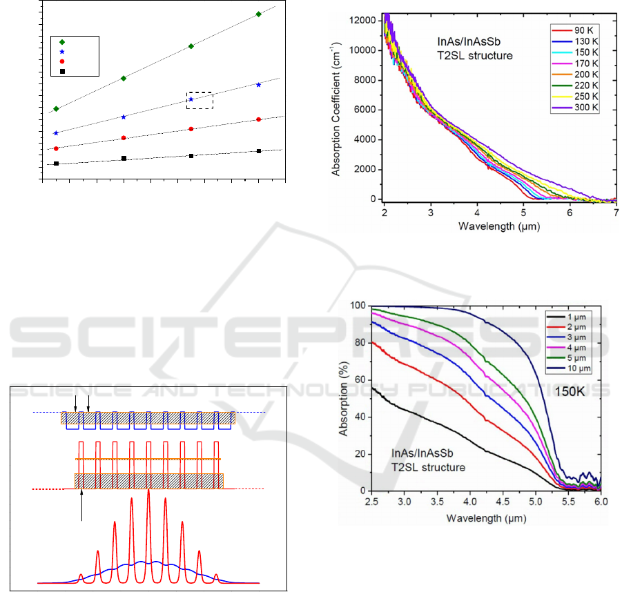
Dedicated structures have been grown by
molecular beam epitaxy (MBE) on GaSb substrate to
perform absorption measurement (Arounassalame,
2022). Figure 5 shows the absorption coefficient for
temperature ranging from 90 K to 300 K. At
λ = 3.4 µm, the absorption coefficient α reaches
4800 cm
-1
at 150 K. At these temperature, Figure 6
displays the calculated absorption for different
absorbing layer thicknesses. For an InAs/InAsSb
T2SL layer thickness equal to 3µm, the absorption
value at λ = 3.4 µm is over 80%.
Figure 5: Absorption coefficient versus wavelength of
InAs (4.5 nm) /InAs
0.65
Sb
0.35
(1.5 nm) T2SL at various
temperatures.
Figure 6: Absorption value versus wavelength of InAs (4.5
nm) /InAs
0.65
Sb
0.35
(1.5 nm) T2SL with different layer
thicknesses.
Such n-type 3µm-thick T2SL structure is the AL
of the XBn detector structure. A adequate BL has to
be chosen to block the electron majority carriers.
The high band-gap energy of AlAs
0.09
Sb
0.91
lattice-
matched to the GaSb substrate (Figure 1) could be a
good candidate as BL. Furthermore, AlSb/InAs
heterostructure presents a staggered type-II band
alignment which should not impede the transport of
hole minority carriers to the CL (Kroemer, 2004).
Barrier Structure for Ga-Free Type-II Superlattice Midwave Infrared Photodetector
23
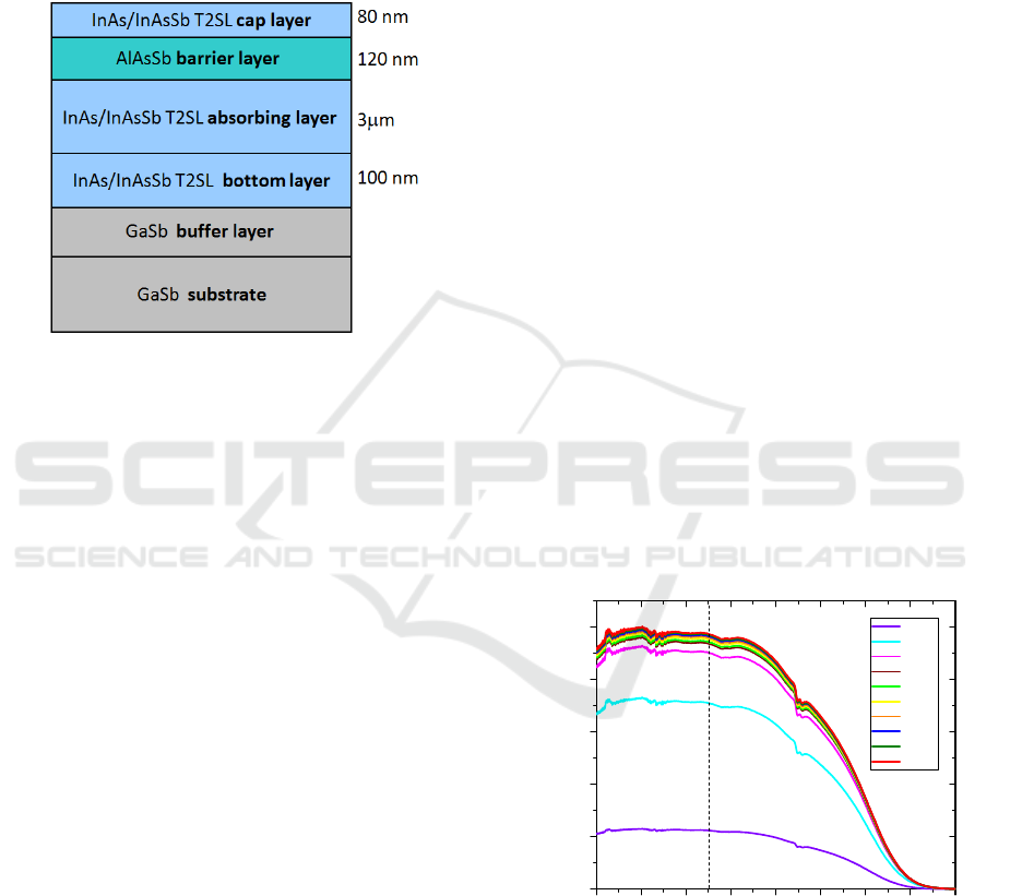
3 FABRICATION OF THE Ga-
Free BARRIER DETECTOR
The Ga-free InAs/InAsSb XBn T2SL detector
structure, presented in Figure 7, was epitaxially
grown on 2-inch n-type (Te-doped) GaSb (100)
substrate by MBE using a 412 RIBER machine.
Figure 7: XBn detector structure : Schematic view of the
different epilayers stacking on GaSb substrate.
The detector structure consists, from top to
bottom, of 80 nm not intentionally doped (nid)
InAs/InAs
0.65
Sb
0.35
T2SL top contact layer (TCL), a
120 nm nid AlAs
0.09
Sb
0.81
barrier layer (BL), a
3000 nm InAs/InAs
0.65
Sb
0.35
T2SL absorber layer
(AL) with a 5 µm targeted cut-off wavelength at 150
K, and finally a 100 nm n-doped (Te) bottom contact
layer (BCL) having the same composition of the AL.
The residual carrier concentration of n-type T2SL
layers has been determined by capacitance-voltage
measurement at 3 x 10
15
cm
-3
at 150K (Zavala-
Moran, 2020). The residual doping of the p-type BL
layer is estimated at 1 x 10
16
cm
-3
.
Before the fabrication of the devices, several
structural and material characterizations, such as
high-resolution X-ray diffraction (HR-XRD) scan,
AFM measurements, photoluminescence (PL) or
time-resolved photoluminescence (TRPL), are
carried out to estimate the quality of the epitaxial
layers and to check the period and the targeted cut-
off wavelength (Zavala-Moran, 2020). If these
characterizations are suitable, with in particular
minority carrier lifetime value as high as 1 µs
(Bouschet, 2021), the T2SL XBn structure is
processed into circular mesa photodetectors with
diameters ranging from 60 to 310 µm using standard
photolithography techniques, wet etching, and metal
evaporation.
Single pixels were fabricated by isotropic wet
chemical etching using a citric acid-based solution.
After the etching step, a polymerized photoresist is
deposited to protect the mesa surface from ambient
air. Metal coatings are applied on both sides of
detectors: Ti/Au on the TCL side and Pd/AuGeNi on
the GaSb substrate.
Next, the samples were wire bonded onto a pin
leadless chip carrier (LCC) and placed in the LN2-
cooled JANIS cryostat ready to perform electrical
and electro-optical measurements. Dark current
density–voltage (J-V) measurements (under a 0-
degree field of view) were performed using a
KEITHLEY 6517A Electrometer to both apply the
bias voltage and measure the current density
delivered by the device while non-calibrated
photoresponse (PR) spectra were recorded by using
a Nicolet-870 Nexus Fourier transform infrared
(FTIR) spectrometer with non-calibrated IR source.
4 CHARACTERIZATION OF THE
Ga-Free BARRIER DETECTOR
Figure 8 displays the front side illuminated
uncalibrated PR spectra obtained at 150 K and for
different biases from -0.1V to -1V. The
measurements show cut-off wavelength at 5µm, the
targeted value at 150K, and quantum efficiency as
high as 55% was measured elsewhere (Bouschet,
2021).
2.02.53.03.54.04.55.05.56.0
0.00
0.20
0.40
0.60
0.80
1.00
Normalized PR spectra
Wavelength (µm)
-0.1 V
-0.2 V
-0.3 V
-0.4 V
-0.5 V
-0.6 V
-0.7 V
-0.8 V
-0.9 V
-1 V
T = 150 K
Figure 8: Normalized Photo-response spectra performed at
150 K for different biases.
At a given wavelength (λ = 3.25 µm for example),
the PR increases gradually and begins to saturate at -
0.4V. This non-zero operating bias value, required to
fully turn on the spectral response, can be explained
by the presence of a valence band offset (VBO) at
PHOTOPTICS 2023 - 11th International Conference on Photonics, Optics and Laser Technology
24
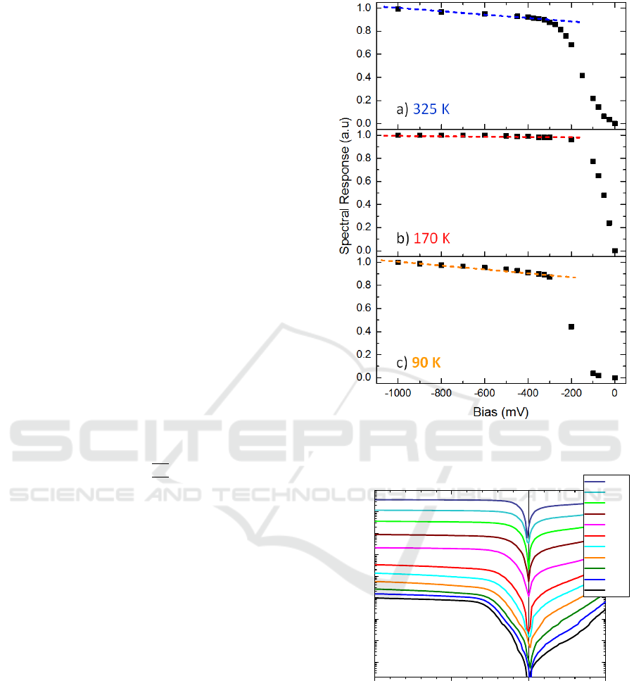
the BL-AL interface, impeding the minority carrier
transport (Righer, 2019). Thus, it is necessary to
apply a minimum bias of -0.40 V, the operating bias
(Vop), to compensate this VBO and allow the
optimal transport of holes.
T2SL is an anisotropic quantum structure in
which the hole minority carriers are strongly
confined in the InAsSb layer (Figure 4). This strong
confinement of the carriers should generate a low
value of the diffusion length and thus, penalize the
PR value. To better understand the hole transport in
T2SL XBn devices, especially the evolution of the
diffusion length as a function of the temperature, we
study the spectral PR versus voltage characteristics
at different temperatures, extracted at a wavelength
equal to 3.25 µm. Figure 9 shows the result obtained
for 325 K (a), 170 K (b), and 90 K (c).
PR behavior seems to be temperature dependant.
At 170 K, the spectral PR value (Figure 9b) appears
to be saturated for higher bias than the operating bias
Vop. This saturation means that the optimal
transport is reached at Vop = - 400 mV with total
collection of minority carriers. It is not the case at
low (90 K, figure 7c) and high (325 K, figure 9a)
temperature showing an unsaturated PR value with a
slope for higher bias than Vop. This behavior could
be linked to the diffusion length L
D
(eq. 2) of hole
minority carriers in the T2SL device.
L
=
𝜇
𝜏 (2)
where k
b
is the Boltzmann constant, µ
h
the hole
mobility and τ the minority carrier lifetime.
Thus, diffusion length is strongly dependant on
mobility and lifetime. Optimum behavior of PR
measurements is obtained at around T = 170K. At
low temperature, the mobility penalizes the diffusion
length (Casias, 2020) whereas it is the lifetime
which reduces it at high temperature
(Arounassalame, 2022).
Figure 10 shows J-V characteristics carried out
for a 210 µm diameter detector in the temperature
range (120 K- 270 K). At the 150 K temperature
operation, dark current density as low as
3x10
-5
A/cm
2
is recorded at operating bias
V = -400mV. Such result has to be improved, since
when compared to the MCT state of the art
photodiode limited by diffusion dark current
(Tennant, 2008), the current is 20 times higher at the
corresponding cut-off wavelength. Nevertheless, this
value remains in agreement with the most recent
results reported on Ga-free T2SL detectors (Ting,
2018 ; Soibel, 2019 ;Wu, 2020).
Figure 9: Uncalibrated PR recorded at 3.25µm as a
function of bias at 325 K (a), 170 K (b), 90 K (c).
-1.0 -0.5 0.0 0.5
10
-8
10
-7
10
-6
10
-5
10
-4
10
-3
10
-2
10
-1
10
0
Current Density (A/cm²)
Voltage (Volts)
270K
250K
230K
210K
190K
170K
160K
150K
140K
130K
120K
Figure 10: Dark current density characteristics of a XBn
InAs/InAsSb T2SL detector at different temperatures from
120 K to 270 K.
From the dark J-V characteristics, transport
regimes in the barrier detector can be identified by
plotting dark current densities at Vop = - 400 mV as
a function of 1/k
B
T (Figure 11). A fit over the
temperature range (150K - 270K) using the
expression A exp(-E
a
/k
B
T) yields an activation
Barrier Structure for Ga-Free Type-II Superlattice Midwave Infrared Photodetector
25
energy E
a
= 230meV which is approximately the
T2SL energy bandgap (E
g
) in this temperature range,
signature of a diffusion limited behavior. In the
temperature range (120K - 145K) the activation
energy is 117 meV, approximately one half of the
T2SL bandgap (E
g
/2), indicating that the dark
current is GR limited, due to the presence of a
depletion region extending into the AL.
40 50 60 70 80 90 100 110 120 130
10
-5
10
-4
10
-3
10
-2
10
-1
290 232 193 166 145 129 116 105 97 89
J
GR
: E
a
= 117 meV
Temperature (K)
exp
J
diff
J
GR
Current Density (A/cm²)
1/k
B
T (eV
-1
)
T
cross
= 149 K
J
diff
: E
a
= 230 meV
Figure 11: Arrhenius plot extracted from J-V curves in
dark conditions at Vop = - 400 mV. Diffusion and
Generation-Recombination dark current regimes are
clearly identified.
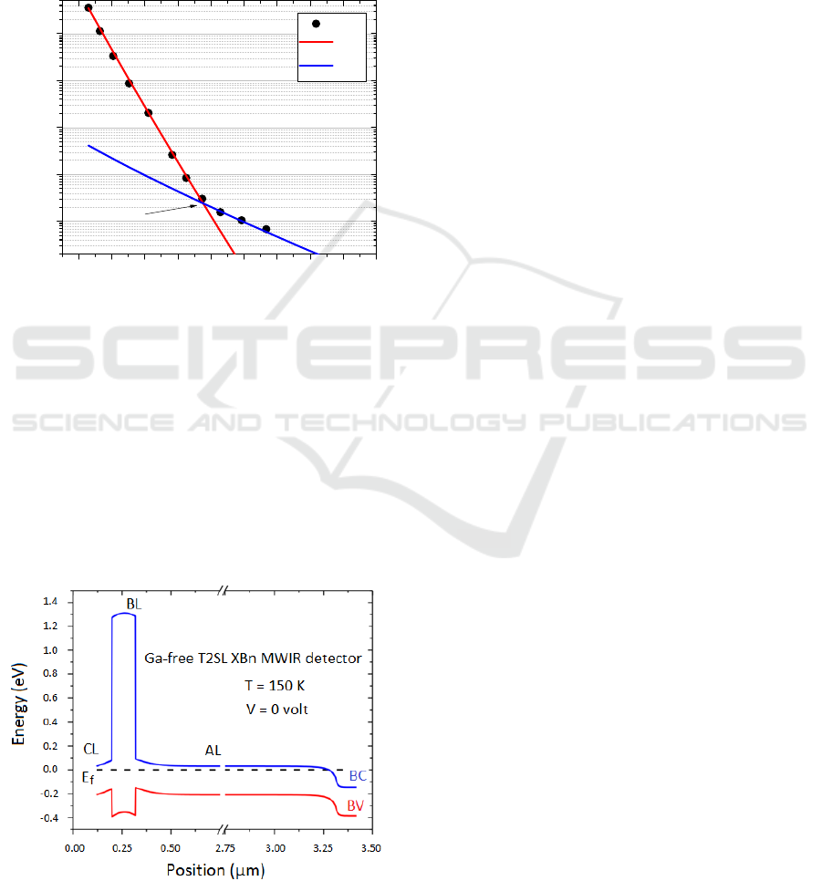
By using residual carrier concentrations, both in
the nid p-type BL (Pres) and in the nid n-type AL
(Nres), extracted from capacitance-voltage (C-V)
measurements (Zavala-Moran, 2020), Figure 12
shows the band diagram at V = 0 volt and T = 150 K
of the considered XBn detector structure which was
deduced from the experimental characterizations
carried out.
Figure 12: Calculated band diagram of the Ga-free T2SL
barrier detector at 150K.
5 CONCLUSIONS
Ga-free InAs/InAsSb T2SL XBn MWIR
photodetector has been fabricated and characterized.
This detector shows cut-off wavelength at 5µm at
150K. The device highlights electrical and electro-
optical performances at this temperature with dark
current density values as low as 3x10
-5
A/cm
2
in
diffusion regime and an optimised photoresponse
behavior. However, the operating bias equal to
-400 mV remains high due to the presence of an
unwanted valence band-offset at the BL-AL
interface. Consequently, the AlAsSb BL has to be
investigated in terms of doping, thickness layer and
alloy composition to overcome this problem. It will
be the subject of forthcoming studies.
ACKNOWLEDGEMENTS
This work was partially funded by the French
“Investment for the Future” program (EquipEx
EXTRA, ANR 11-EQPX-0016) and by the French
ANR under project HOT-MWIR (N° ANR-18-
CE24-0019-01).
REFERENCES
Arounassalame, V.; Bouschet, M.; Alchaar, R.; Ferreira,
R.; Carosella, F.; Ramiandrasoa, A.; Perez, J.-P.; Péré-
Laperne, N.; Christol, P.; Ribet-Mohamed, I., 2022.
Anisotropic transport investigation through different
etching depths in InAs/InAsSb T2SL barrier midwave
infrared detector. Infrared Physics Technology, 126,
104315.
Bouschet, M.; Zavala-Moran, U.; Arounassalame, V.;
Alchaar, R.; Bataillon. C.; Ribet-Mohamed, I.; De
Anda-Salazar, F.; Perez, J.P.; Péré-Laperne, N.;
Christol, P., 2021. Influence of pixel etching on
electrical and electro-optical performances of a Ga-
free InAs/InAsSb T2SL barrier photodetector for mid-
wave infarred imaging. Photonics 8, 194.
Casias, L.K.; Morath, C.P.; Steenbergen, E.H.; Umana-
Membreno, G.A.; Webster, P.T.; Logan, J.V.; Kim,
J.K.; Balakrishnan, G.; Faraone, L.; Krishna, S., 2020.
Vertical carrier transport in strain-balanced
InAs/InAsSb type-II superlattice material. Applied
Physics Letters 116, 182109.
Klipstein, P., Klin, O., Grossman, S., Snapi, N.,
Lukomsky, I., Aronov, D., Yassen, M., Glozman, A.,
Fishman, T., Berkowicz, E., Magen, O., Shtrichman,
I., Weiss, E., 2011. XBn barrier photodetectors based
on InAsSb with high operating temperatures, Optical
Engineering, 50, 061002
PHOTOPTICS 2023 - 11th International Conference on Photonics, Optics and Laser Technology
26

Kroemer, H., 2004. The 6.1A family (InAs, GaSb, AlSb)
and its heterostructure : a selective review, Physica E
20, 196.
Lackner, D., Steger, M., Thewalt, M.L.W., Pitts, O.J.,
Cherng, Y.T., Watkins, S.P., Plis, E., Krishna, S.,
2012. InAs/InAsSb strain balanced superlattices for
optical detectors: Material properties and energy band
simulations, Journal of Applied Physics 111, 034507
Maimon, S., Wicks, G., 2006. nBn detector, an infrared
detector with reduced dark current and higher
operating temperature, Applied Physics Letters, 89,
151109.
Rhiger, D.; Smith, E.P., 2019. Carrier transport in the
valence band of nBn III–V superlattice infrared
detectors. Journal of Electronic Material 48, 6053
Soibel, A.; Ting, D.Z.; Rafol, S.B.; Fisher, A.M.; Keo,
S.A.; Khoshakhlagh, A.; Gunapala, S.D., 2019. Mid-
wavelength infrared InAsSb/InAs nBn detectors and
FPAs with very low dark current density. Applied
Physics Letters 114, 161103.
Steenbergen, E.H., Cellek, O.O., Lubyshev, D., Qiu, Y.,
Fastenau, J.M., Liu, A.W.K., Zhang, Y.H., 2012.
Study of the valence band offsets between InAs and
InAs
1-x
Sb
x
alloys, Proc. SPIE 8268, 82680K
Tennant, W.E.; Lee, D.; Zandian, M.; Piquette, E.;
Carmody, M., 2008. MBE HgCdTe technology: A
very general solution to IR detection, described by
“Rule 07”, a very convenient heuristic. Journal of
Electronic Material, 37, 1406.
Ting, D.Z.; Soibel, A.; Khoshakhlagh, A.; Rafol, S.B.;
Keo, S.A.; Höglund, L.; Fisher, A.M.; Luong, E.M.;
Gunapala, S.D., 2018. Mid-wavelength high operating
temperature barrier infrared detector and focal plane
array. Applied Physics Letters 113, 021101.
Webster, P. T., Riordan, N.A., Liu, S., Steenbergen, E.H.,
Synowicki, R.A., Zhang, Y.-H., 2015. Absorption
properties of type-II InAs/InAsSb superlattices
measured by spectroscopic ellipsometry, Applied
Physics Letters 106, 061907
Wu, D.; Li, J.; Dehzangi, A.; Razeghi, M., 2020. Mid-
wavelength infrared high operating temperature pBn
photodetectors based on type-II InAs/InAsSb
superlattice. AIP Advances 10, 025018.
Zavala-Moran, U.; Bouschet, M.; Perez, J.P.; Alchaar, R.;
Bernhardt, S.; Ribet-Mohamed, I.; De Anda-Salazar,
F.; Christol, P., 2020. Structural, optical and electrical
characterizations of midwave infrared Ga-free Type-II
InAs/InAsSb superlattice barrier photodetector.
Photonics 7, 76.
Barrier Structure for Ga-Free Type-II Superlattice Midwave Infrared Photodetector
27
