
Detection of <12 µV
RMS
Extracellular Action Potential and Local
Field Potential by Optimum Design of a Single Pixel
Electrolyte-Oxide-MOSFET Interface in CMOS 28 nm
David Tomasella
a
, Elia Vallicelli
b
, Andrea Baschirotto
c
and Marcello De Matteis
d
Department of Physics, University of Milano Bicocca, Piazza della Scienza 3, Milano, Italy
Keywords: Biological Neural Networks, Biosensors, Neural Engineering, Analog Integrated Circuits, Low-Noise
Amplifier.
Abstract: Microelectrode-Arrays (MEAs) allow monitoring thousands of neurons/mm
2
by sensing: extracellular Action
Potentials and (in-vivo) Local Field Potentials. MEAs arrange several recording sites (or pixels) in a spatial
grid, planarly and capacitively coupled with in-vitro cell cultures and/or integrated in electrocorticography
grids. This paper focuses on Electrolyte-Oxide MOS Field-Effect-Transistors (EOMOSFET) MEAs for cell-
level recording and presents a complete model of the neuron-electronics junction that reduces to a single
electrical scheme all the biological (the neuron) and physical layers (the electrolyte, the Diffuse/Helmoltz
capacitances, the oxide and the MOS transistor) composing the interface. This allows to predict the noise
power coming from biological environment (electrolyte bath) and to optimize all electrical parameters with
the main aim to minimize the final sensing Noise Figure and thus enhance the acquisition Signal-to-Noise-
Ratio. Frequency domain simulations from the proposed model demonstrates that there is an optimum design
point for all parameters involved in the building EOMOSFET pixel that allows to perform >9 dB Signal-to-
Noise-Ratio at <12 µV
RMS
extracellular neuro-potentials power at the electrode node. This will finally enable
high-resolution recording of ultra-weak neuro-potentials signals flowing by the electrolyte cleft that have not
been never explored adopting planar capacitive coupling interfaces.
1 INTRODUCTION
There is a rather large lack of information between
neuron membrane electrical activity of single
neurons, and physiological or whole brain
behavioural events. To fill this gap, we need to
understand the activity of individual neurons and how
it contributes to neural circuits functioning. Such
ambitious perspective cannot be achieved by
macroscale neural recording techniques
(electroencephalogram, magnetic resonance, etc.),
nor by patch clamps (monitoring single cell unit). One
of the best options is to adopt Microelectrode-Arrays
(MEAs, (Obien, 2015; Thomas, 1972; Pine, 1980))
that allow monitoring thousands of neurons/mm
2
by
sensing: extracellular Action Potential (EAP in 300
a
https://orcid.org/0000-0001-8413-5751
b
https://orcid.org/0000-0003-0905-151X
c
https://orcid.org/0000-0002-8844-5754
d
https://orcid.org/0000-0003-1061-1262
Hz – 5 kHz bandwidth) and (in-vivo) Local Field
Potential (LFP up to 300 Hz bandwidth). They are
used as planar probes in neuron cells cultures forming
a cell-electrode capacitive coupling. Implanted
MEAs are typically needle-shaped probes that deeply
penetrate the cortex for tissues recording/stimulating
and for increasing proximity and signals detection
rate.
Both in-culture and implantable MEAs can be
integrated in commercial CMOS silicon substrates
with an additional post-processing step consisting on
covering CMOS metal aluminium electrodes by
noble metal films (Pt/Au (Gross, 1982)) or dedicated
oxide layers (TiO2 (Cianci, 2012)). Active MEAs
embed both analog signal processing channels (by
neural amplifier, low-pass filter for antialiasing and
A-to-D conversion) and digital circuits synthesizing
66
Tomasella, D., Vallicelli, E., Baschirotto, A. and De Matteis, M.
Detection of <12 VRMS Extracellular Action Potential and Local Field Potential by Optimum Design of a Single Pixel Electrolyte-Oxide-MOSFET Interface in CMOS 28 nm.
DOI: 10.5220/0010346300660076
In Proceedings of the 14th International Joint Conference on Biomedical Engineering Systems and Technologies (BIOSTEC 2021) - Volume 1: BIODEVICES, pages 66-76
ISBN: 978-989-758-490-9
Copyright
c
2021 by SCITEPRESS – Science and Technology Publications, Lda. All rights reserved
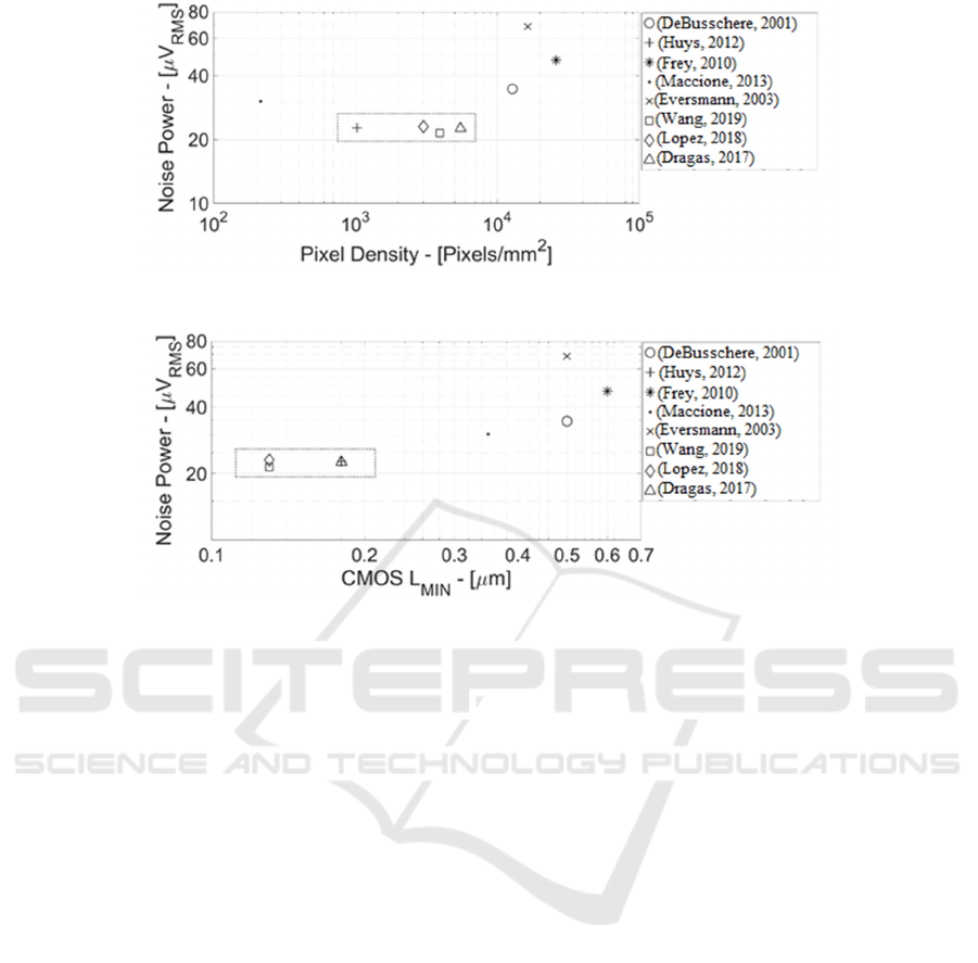
Figure 1: Microelectrode Arrays State-of-the-Art (Noise Power vs. Electrodes/Pixels Density).
Figure 2: Microelectrode Arrays State-of-the-Art (Noise Power vs. CMOS Minimum Channel Length).
advanced Digital Spikes Detection ((Vallicelli, 2018;
Shadid, 2009) DSD) algorithms. DSDs exploit the
large array spatial resolution for separating relevant
extracellular events from background noise by spatial
correlation post-processing algorithms. They perform
complex digital algorithm that require a certain
computing power leading to a non-negligible
dynamic power consumption and preventing
integration in the same MEA silicon area.
Despite outstanding advancements in neural probes
development, there are still many phenomena that
state-of-the-art MEA technology cannot observe at
high spatial resolution:
at membrane level, subthreshold events, such as
synaptic potentials can influence cell rest status
without producing an action potential;
propagation of the action potentials (AP) in
axons, the backpropagation of AP in the
dendrites and the generation of dendritic spikes,
and weak extracellular synaptic field potential;
traces of membrane oscillations in the
extracellular space, never observed by planar
probes since they require single-cell patch
recording techniques.
Simply speaking, these events and phenomena cannot
be observed because noise power floor in cell-
electrolyte-electrode-electronics junction, is to date
higher than the signal power of those extracellular
neuro-potentials carrying information coming from
subthreshold or ultra-weak events.
Figure 1 shows some of most relevant MEAs state-
of-the-art (DeBusschere, 2001; Huys, 2012; Frey,
2010; Maccione, 2013; Eversmann, 2003; Wang,
2019; Lopez, 2018; Dragas, 2017) in terms of noise
power (in µV
RMS
measured at the electrode node) vs.
Pixel Density (electrodes count per mm
2
). Both axes
are in log scale. There is a clear trend of noise power
increasing with larger pixels density. Such trend is
justified by the smaller electrode area (at higher pixel
density) that increases flicker noise power coming
from both the TiO
2
/Metal film charge traps and the
MOS transistor (MOST) placed just below the
electrode.
In other words, to decrease the noise power and to
detect sub-threshold events, it is necessary to increase
the area of the single electrode but this would again
lead to a reduction of the pixel density, degrading the
neural recording spatial resolution.
Morevoer, this approach has already reached the
point of maximum efficiency because ref. (Huys,
2012; Dragas, 2017) in CMOS 0.18 µm and ref.
(Wang, 2019; Lopez, 2018) in CMOS 0.13 µm
(rectangular box in both Figure 1 and Figure 2) show
practically the same noise power (i.e. approximately
22 µV
RMS
) at the electrode equivalent node.
Detection of <12 VRMS Extracellular Action Potential and Local Field Potential by Optimum Design of a Single Pixel
Electrolyte-Oxide-MOSFET Interface in CMOS 28 nm
67
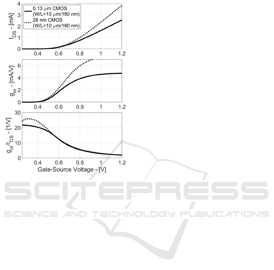
Figure 3: Drain-Source Current (I
DS
), Transconductance
(g
m
) and Efficiency (g
m
/I
DS
) in CMOS 0.18 µm and 28 nm
for Standard-Process MOST.
Furthermore, at such noise power levels,
increasing electrode area (and thus reducing pixel
density) does not involve a significant 1/f (flicker)
noise power reduction because MOS transistors
thermal noise (in first approximation independent on
electrode area and dependent on MOST dc current)
becomes more dominant.
More specifically in-band thermal noise power
spectral density is inversely proportional to the MOS
transistor transconductance (g
m
). Such g
m
is
proportional to the current consumption, that (in bio-
signals processing analog stages) operate the MOST
with few µA current (Harrison, 2003). Thus the
efficiency of the MOST (defined as g
m
/I
DS
ratio
(Sansen, 2007) or in other words the amount of g
m
that can be synthesized by a MOST operating at a
certain drain-source current I
DS
) becomes a key
parameter for both noise and power minimization in
next generation MEAs.
Unfortunately, all most performant MEAs (Huys,
2012; Wang, 2019; Lopez, 2018; Dragas, 2017) are
implemented in very old CMOS technologies (0.13
µm processes nodes and beyond for flicker noise
power reduction), where MOST efficiency is very
much lower than nm-range CMOS nodes.
Figure 2 shows state-of-the-art MEAs noise
power vs. CMOS process generation in terms of
minimum MOST channel length.
Maximum (sub-threshold voltage) MOST
efficiency in 0.13 µm (or 0.18 µm CMOS node) is
about 20 V
-1
, whereas 28 nm CMOS improves g
m
/I
DS
up to 26 V
-1
, resulting in approximately +3dB
electrode noise attenuation at same current.
These last considerations are validated in Figure
3, where MOST Drain-Source Current (I
DS
),
Transconductance (g
m
) and Efficiency (g
m
/I
DS
) are
plotted vs. gate-source voltage in CMOS 0.13 µm and
28 nm for Standard-Process MOSTs.
Moreover, older CMOS processes increases
system complexity (Baschirotto, 2009; De Matteis,
2006) and harness, because Digital Spikes Detection
stages cannot be on-chip integrated due to its very
high dynamic power in low scaled-down CMOS
nodes. Effectively such power will be incompatible
with a stable spatial temperature distribution for cell
integrity in neuron cultures and with the limited
power budget required by the portability of
implantable devices.
In this context, this paper proposes a dedicated
design of EOMOSFET MEAs (for the case of a single
recording site/pixel and that can be easily extended to
spatial matrix MEAs) that efficiently sets the basis for
definitely overcome the above issues by:
adopting the CMOS 28 nm technology node and
then including in the model the technology node
parameters like dielectric constant, gate
capacitance per unit area, sub-threshold slope
factor coefficient, etc. This enables two key
improvements:
o to take advantage of the higher g
m
(and
lower thermal noise power spectral
density) for a given current of analog
CMOS 28 nm SP MOST against 0.13 µm
and beyond;
o to use on-chip DSD stages without
exceeding in extra-power (by ultra-low
digital dynamic power for Standard-
Process MOST);
rejecting the flicker noise by maintaining the
electrode area equal to 100 µm
2
(approximately
three times lower than neuron area) enabling
about 1 k neuron recording for 1 mm
2
active
MEA area.
This paper is organized as follows. Section 2
describes the cross-section layers of the CMOS 28 nm
EOMOSFET pixel and all relevant signal/noise
transfer functions as a function of the interface
electrical parameters. Section 3 presents the
BIODEVICES 2021 - 14th International Conference on Biomedical Electronics and Devices
68
Figure 4: EOMOSFET Single Pixel Cross-Section.
simulation results of the model and the selected
design point that allows to perform >9 dB SNR with
< 12 µV
RMS
neuro-potentials signals power. At the
end of the paper conclusions will be drawn.
2 EOMOSFET CROSS-SECTION
AND ELECTRICAL
CHARACTERISTICS
EOMOSFET biosensors are spatially organized in a
matrix of pixels. The proposed model is based on the
the single pixel electrical scheme shown in Figure 4.
The neuron population and the silicon die separated
by an electrolyte bath (NaCL at 0.1 Moles
concentration). The TiO
2
post-processing layer
(Cianci, 2012) isolates the silicon circuits from the
biological environment. The extracellular ionic
currents flow by the electrolyte equivalent resistance
(R
E
) inducing a small voltage variation. Thus, the
voltage across R
E
is coupled with the TiO
2
capacitance (C
TiO2
) by the C
D
-C
H
series, where C
D
and
C
H
are the double-layer region capacitances (Diffuse
and Helmotz layers capacitances, respectively
(Massobrio, 2016)). Just beneath the TiO
2
there is an
on-chip metal electrode, whose area (A
ELE
) is in this
case 100 µm
2
(here M
SENSE
area is 50% lower to
maintain the imaging resolution). This oxide layer has
approximately 6 nm thickness and builds a specific
series capacitance (C
TiO2
).
Notice that this scheme is referred to the worst
case scenario of scarce neuron-chip adhesion
(Massobrio, 2016), where neuro-potentials signals
are very weak and are spread across the electrolyte
bath. Thus the voltage source (v
in
) models both EAP
and LFP signals.
Thus, the equivalent capacitance (C
DHT
) between
the cells and the MOS transistor (MOST) M
SENSE
gate
is given by eq. (1):
𝐶
/
/
/
(1)
C
D
and C
H
capacitances depend on the charge
concentration at the electrolyte-oxide interface.
More specifically such Helmoltz and diffuse
layers capacitances can be calculated using the metal
electrode area (A
ELE
), the water permittivity
(ε
w
=78.4ꞏε
0
where ε
0
is the vacuum permittivity equal
to 8.85 pF/m) and two physical lengths L
D
(Deybe
Detection of <12 VRMS Extracellular Action Potential and Local Field Potential by Optimum Design of a Single Pixel
Electrolyte-Oxide-MOSFET Interface in CMOS 28 nm
69
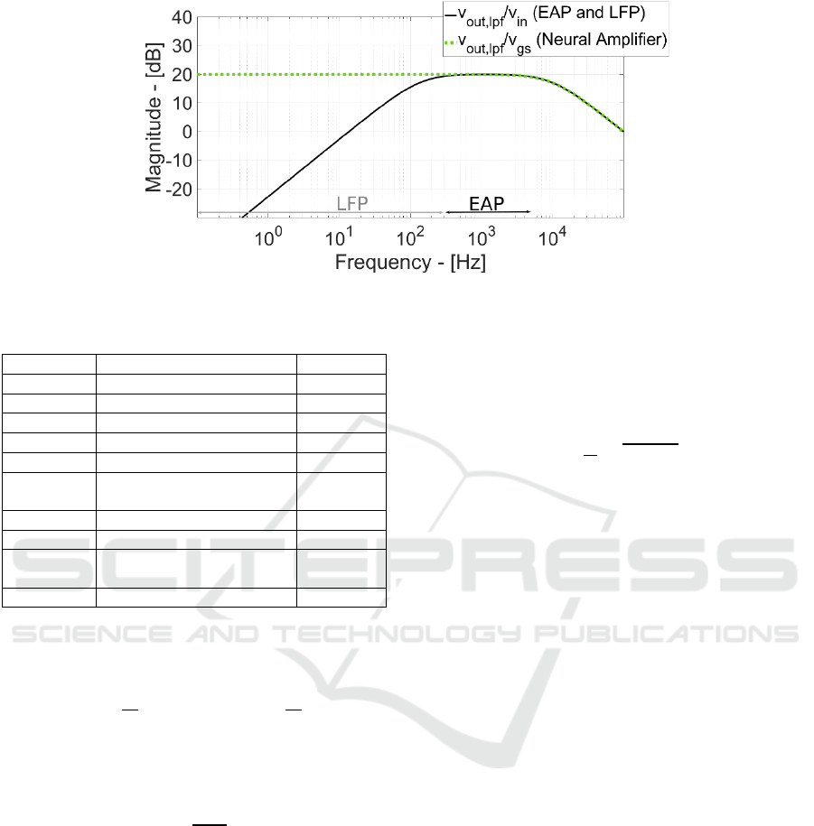
Figure 5: Signal Frequency Response.
Table 1: Neuron-Silicon Electrical Model Parameters.
Parameter Explanation Value
A
ELE
Metal Electrode Area 100 µm
2
R
E
Electrolyte Bulk Resistance 125 kΩ
C
D
Stern Ca
p
acitance 35.9
p
F
C
H
Helmotz Ca
p
acitance 17.3
p
F
C
T
TiO2 Ca
p
acitance 3.3
p
F
M
SENSE
W
S
/L
S
M
SENSE
Aspect Ratio
50 µm / 1
µ
m
g
ms
M
SENSE
Transconductance 50
µ
A/V
r
ds
M
SENSE
Out
p
ut Resistance 187 kΩ
τ
LP
Low-Pass Filter Dominant
Time-Constant
100 µs
(
10 kHz
)
R
F
Pseudo-Resistor Value 5 GΩ
length, equal to 1 nm) and x
2
(Stern length, equal to 2
nm) depending on the electrolyte-oxide interface
(Massobrio, 2016).
𝐶
∙𝐴
𝑎𝑛𝑑 𝐶
∙𝐴
(2)
The TiO
2
isolation layer capacitance has 45ꞏε
0
and 6
nm permittivity and thickness, respectively (Cianci,
2012):
𝐶
∙𝐴
(3)
Table 1 resumes the main values of the neuron-
electronics junction electrical model.
Hence, the M
SENSE
MOST is the core of a
dedicated neural Low-Noise-Amplifier (LNA) that
drives an ideal low-pass filter whose main aim is to
limit the signal bandwidth at 10 kHz. M
SENSE
small-
signal current is proportional (by its transconductance
(g
ms
)) to the induced extracellular AP and LFP (v
in
).
The M
SENSE
MOST is here biased by a feedback
pseudo-resistor (M
F
) to synthesize a very high
resistance (R
F
in the order of few GΩ) that sets the
low frequency pole (where LNA bandwidth starts).
The electrolyte bulk plays a key role for both
signal and noise transfer function. Its equivalent
resistance R
E
depends on the electrolyte bulk
conductibility k
’
and on the metal electrode area A
ELE
(Deen, 2006) as follows:
𝑅
∙
𝜋/𝐴
(4)
Assuming the same number of carriers (N
C
=N
P
=N
N
)
for both positive (N
P
, cations) and negative (N
N
,
anions) charges, then the bulk electrolyte
conductivity is related with the moles concentration
(N
MOL
) and the water density (ρ=1000 Kg/m
3
) as
expressed in eq. 5 (Park, 2016):
𝑘
𝑞∙
𝜇
∙𝑁
𝜇
∙𝑁
𝑞∙
𝜇
𝜇
∙𝑁
𝑞∙
𝜇
𝜇
∙𝜌∙𝑁
(5)
where µ
P
-µ
N
are the mobility coefficients for cations-
anions, respectively. Thus, the bulk electrolyte
conductivity is equal to 12.6 mA/(Vꞏm) and the bulk
resistance R
E
is then 125 kΩ at 100 mM.
2.1 EAP and LFP Signal Transfer
Function
Previous considerations definitively fix the numerical
values of all parameters involved in neuron-
electronics junction as a function of the physical size
and characteristics of the several layers composing
the EOMOSFET pixel. It is thus possible to calculate
the small signal transfer function for all relevant
signal and noise contributions. This will provide a
frequency domain map of the achievable Signal-to-
Noise-Ratio and, more importantly, a clear limit in
terms of maximum allowable noise power for analog
stages with the main aim to avoid significant SNR
degradation.
Input signal v
in
includes both EAP and LFP neuro-
potentials. The transfer function between input signal
BIODEVICES 2021 - 14th International Conference on Biomedical Electronics and Devices
70
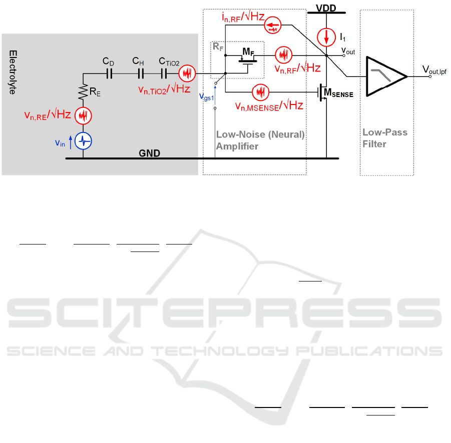
Figure 6: Noise Sources Frequency Response.
(v
in
) and Low-Pass Filter (LPF) output node (v
out,lpf
/v
in
in Laplace domain) is given by eq. 6:
,
𝑠
∙
∙
∙
∙
∙
∙
∙
∙
∙
∙
(6)
where g
ms
and r
ds
are M
SENSE
MOST small-signal
parameters, and τ
LP
is the low-pass filter dominant
time constant (fixing the LPF -3dB passband at 10
kHz). Figure 5 shows the corresponding eq. 6
frequency response and includes the analog signal
processing (Neural Amplifier and Low-Pass Filter)
frequency response. Thanks to the very high
resistance synthesized by pseudo-resistors (5 GΩ),
the dominant pole time constant (C
HDT
ꞏR
F
/(g
ms
ꞏr
ds
))
has a frequency of 136 Hz and more importantly the
gain is higher than 0 dB (i.e.) from 13 Hz (channel
starts to amplify the input signal) enabling recording
of ultra-weak slow-oscillation and/or low-frequency
neuro-potentials.
2.2 Noise Transfer Function
Figure 6 shows the EOMOSFET pixel equivalent
circuit with the most relevant noise sources (coming
from electrolyte resistance R
E
(v
n,Re
), TiO
2
film
(v
n,TiO2
), feedback pseudo-resistor R
F
(v
n,RF
) and
sensing MOST M
SENSE
(v
n,MSENSE
)). The analog front-
end is composed by the cascade of a neutral Low-
Noise-Amplifier (LNA, for neural signal read-out and
amplification) driving a Low-Pass Filter (LPF) at 10
kHz -3dB bandwidth for signal selection and out-of-
band noise rejection. The amount of noise at the
output of the analog signal processing chain (v
out,lpf
,
i.e. the LPF output node) depends on the specific
noise power of each noise source and the frequency
response associated to each noise source.
2.2.1 R
E
Thermal Noise
The electrolyte resistance (R
E
) generates thermal
noise (v
n,RE
) whose in-band power spectral density is
given by eq. 7:
〈
,
〉
4∙𝑘∙𝑇∙𝑅
(7)
k and T are Boltzman constant and temperature (300
K) and R
E
is 125 kΩ as reported in eq.4 and Table 1.
The v
out
/v
n,RE
transfer function (in Laplace domain)
gives the total amount of voltage signal at the output
of the filter as a function of C
HDT
capacitance (C
H
, C
D,
and C
TiO2
serie), the feedback pseudo-resistor (R
F
)
and M
SENSE
MOST main small-signal parameters
(transconductance (g
ms
) and output resistance (r
ds
)):
,
,
𝑠
∙
∙
∙
∙
∙
∙
∙
∙
∙
∙
(8)
Figure 7 illustrates the corresponding frequency
response and demonstrates that R
E
thermal noise has
the same signal transfer function. This is even
demonstrated by Figure 8 where the noise power
spectral density (PSD) for every EOMOSFET noise
source with the total noise PSD is plotted.
Effectively R
E
noise PSD (green line) perfectly
overlap the v
in
signal bandwidth and thus it is one of
the most relevant ineliminable noise sources in
EOMOSFET pixels and more generally in planar
capacitively-coupled neural probes/MEAs.
2.2.2 TiO
2
Flicker Noise
TiO
2
film (used to separate or couple the biological
environment from silicon chip) mainly generates
Detection of <12 VRMS Extracellular Action Potential and Local Field Potential by Optimum Design of a Single Pixel
Electrolyte-Oxide-MOSFET Interface in CMOS 28 nm
71
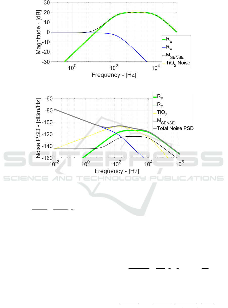
Figure 7: Noise Sources Frequency Response.
Figure 8: Output Noise PSD.
flicker noise. Its power source is inversely
proportional to the frequency f, as follows:
〈
,
〉
,
∙
(9)
where k
pf,TiO2
is the specific flicker constant and C
TiO2
is the equivalent TiO
2
capacitance. v
n,TiO2
has the
same transfer function as v
n,RE
(eq. 8). In this model
TiO
2
has been preferred to other neuron-silicon
junction coupling options, because it has lower flicker
noise power comparing with Pt/Au noble metal films
that can exhibit an 1/f
2
noise, increasing the low
frequency noise power at the output of the neutral
amplifier.
Nonetheless the intrinsic neuron-electronics
junction ac-coupling allows some filtering of TiO
2
flicker at low frequency. Afterwards, starting from
136 Hz, v
n,TiO2
frequency response has 20 dB gain but,
at the same time, TiO
2
1/f noise behaviour has already
reduced its noise power. This generate a TiO
2
noise
PSD maximum at 132 Hz and, after this frequency,
the circuit attenuates the TiO
2
flicker noise power.
2.2.3 M
SENSE
Noise
The main noise contributions of the neural amplifier
come from M
SENSE
and R
F
(feedback pseudo-resistor).
M
SENSE
is a MOST biased in subthreshold region
synthesizing 50 µA/V transconductance g
ms
. This
value allows to minimize M
SENSE
thermal noise at few
µA current consumption and thus making feasible the
integration of the proposed EOMOSFET setup in
thousands of pixels resolution spatial grid/matrix
without excess of power. The equivalent model for
M
SENSE
noise source is:
〈
,
〉
∙
∙
∙4∙𝑘∙𝑇∙
(10)
where k
F
is the CMOS 28 nm flicker constant and W
S
and L
S
are M
SENSE
width and length. The transfer
function associated to the v
n,MSENSE
noise source is:
,
,
𝑠
≅
∙
∙
∙
∙
∙
∙
∙
∙
∙
∙
(11)
BIODEVICES 2021 - 14th International Conference on Biomedical Electronics and Devices
72

At low frequency (<< 13 Hz) the C
HDT
capacitor
behaves like an open circuit. M
SENSE
is then diode-
connected and thus its noise source transfers to the
output by unitary gain. At very high frequency (>> 13
Hz) C
HDT
features very low impedance (ideally a
short circuit), then the feedback is broken and
v
n,MSENSE
is directly applied between M
SENSE
gate and
ground. Thus output voltage noise is 20 dB higher.
One of the objectives of this model is to minimize
such noise contribution by acting on both M
SENSE
area
(WꞏL for flicker noise power reduction, here set at 50
µm
2
) and transconductance (for thermal noise power
reduction at 50 µA/V resulting in 14.8 nV/√Hz in-
band noise PSD).
2.2.4 R
F
Pseudo-resistor Noise
To enhance the pass-band gain of the EOMOSFET
pixel and to enable observation of ultra-weal ultra-
low frequency neuro-potential signals, the feedback
resistance must be in the GΩ order. Integrated
resistors in silicon technologies are not a feasible
option for such a large resistance value, hence this
model adopts a MOST in off region (pseudo-resistor)
where gate-source nodes are shorted, preventing any
conductive channel between drain and source and
exploiting the parasitic diodes formed by source-bulk
and drain-bulk junctions. Such diodes are
automatically biased in reverse region synthesising a
very high resistance (5 GΩ in this case). Starting from
these considerations, the R
F
pseudo-resistor noise
source has two main noise sources: shot (from diodes)
and flicker as follows:
〈
,
〉
∙
∙
(12)
〈
,
〉
2∙𝑞∙𝐼
(13)
where W
F
and L
F
are width and length of the pseudo-
resistor MOST, I
LEAK
is the leakage current mainly
coming from M
SENSE
gate oxide and approximately
equal to few pA. Notice that since R
F
is connected in
feedback, its noise is relevant at very low frequency
(< 136 Hz). So, this effect will be important in
13 Hz – 136 Hz bandwidth. The transfer functions for
v
n,RF
and i
n,RF
noise sources are respectively:
,
,
𝑠
≅
∙
∙
∙
∙
∙
∙
∙
∙
∙
∙
(14)
,
,
𝑠
≅𝑅
∙
∙
∙
∙
∙
∙
∙
∙
∙
∙
∙
(15)
Table 2: Noise Summary.
Bandwidth Noise Source Value [
µ
V
RMS
]
< 300 Hz
R
E
5.5
TiO
2
15.7
R
F
10.4
M
SENSE
1.73
Total Noise 19
300 Hz – 5 kHz
R
E
30
TiO
2
27.2
R
F
1
M
SENSE
9.5
Total Noise 42
< 5 kHz
R
E
30.6
TiO
2
31.4
R
F
10.4
M
SENSE
9.66
Total Noise 46.08
3 NOISE SUMMARY AND
SIGNAL-TO-NOISE-RATIO
The small-signal electrical and analytical model
based on Figure 6 scheme allow to easily evaluate the
noise and signal behaviour across the EOMOSFET
pixel.
More in details, by reducing the M
SENSE
MOST
thermal/flicker noise power and taking into account
both shot and flicker noise sources coming from MF
pseudo-resistor, the presented setup enables very low
noise performances (1.9 µV
RMS
and 4.2 µV
RMS
) at the
electrode (or at the M
SENSE
gate node).
Table 2 presents the noise summary of this
specific setup where, in both LFP and EAP
bandwidths, dominant noise contributions come from
electrolyte bath (thermal) and TiO
2
(flicker) coupling.
In other words by a dedicated design of the
interface in terms of both biological and circuital
electrical parameters, it is possible to set MOSTs
(M
SENSE
and M
F
) dc current and aspect ratio with the
main aim to minimize read-out noise power and in
first approximation remaining with the only interface
noise due to the electrolyte-electrode junction.
Effectively in LFP bandwidth, total noise
(measured at the low-pass filter output node) is 19
µV
RMS
(with 5.5 µV
RMS
R
E
noise power and 15.7
µV
RMS
TiO
2
noise power, respectively).
In EAP bandwidth, total output noise is 42 µV
RMS
when R
E
and TiO
2
have 30 µV
RMS
and 27.2 µV
RMS
noise power, respectively.
About SNR performances, Table 3 reports a final
resume of the achieved SNR in both EAP and LFP
bandwidths, also including Noise Figure
performances.
Detection of <12 VRMS Extracellular Action Potential and Local Field Potential by Optimum Design of a Single Pixel
Electrolyte-Oxide-MOSFET Interface in CMOS 28 nm
73
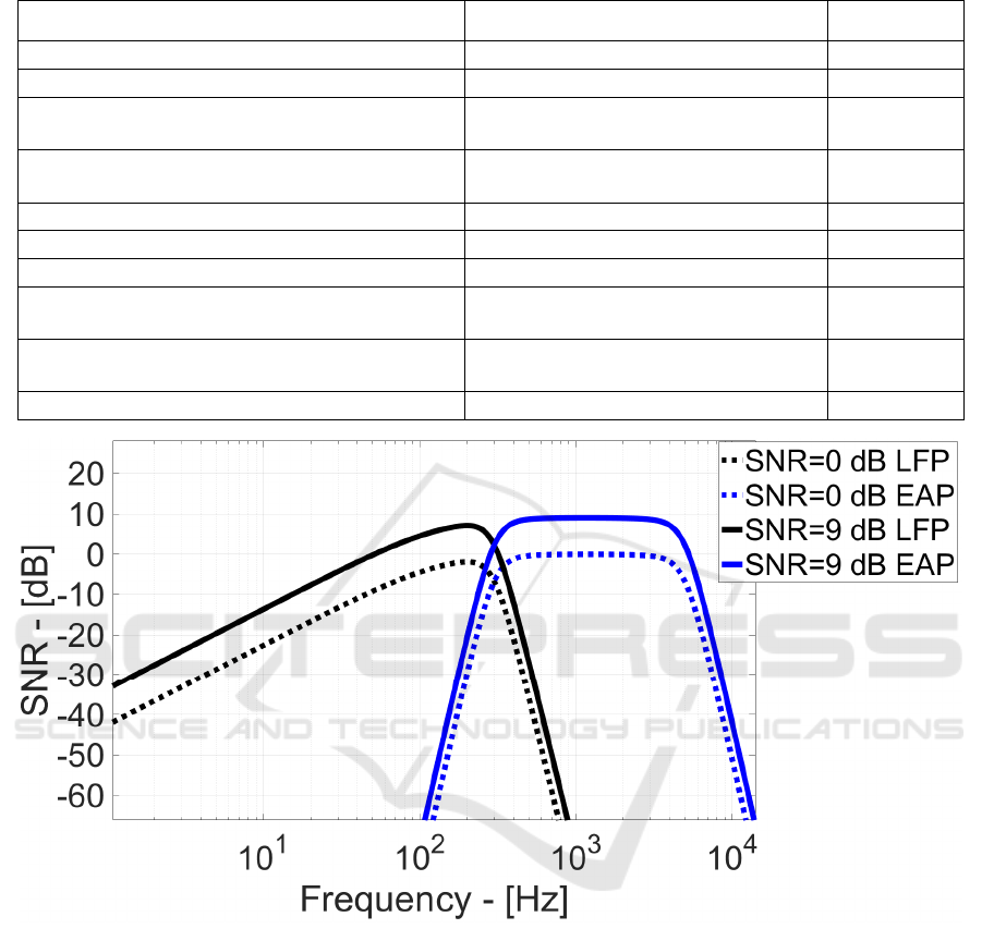
Table 3: Noise Summary, SNR and Noise Figure.
Parameter Explanation Value
< 300 Hz Output Noise LFP Bandwidth Output Noise 19 µV
RMS
< 300 Hz Electrolyte Noise LFP Bandwidth TiO
2
+R
E
Output Noise 16.63 µV
RMS
< 300 Hz Electrode SNR at v
in
=10 µV
RMS
LFP Bandwidth SNR at the Electrode
(considering only TiO
2
and R
E
Noise)
15.5 dB
< 300 Hz LPF SNR
LFP Bandwidth Output SNR
(at the LPF Output Node)
14.42dB
< 300 Hz NF LFP Noise Figure 1.15 dB
300 Hz - 5 kHz Output Noise EAP Bandwidth Output Noise 42 µV
RMS
300 Hz - 5 kHz Electrolyte Noise EAP Bandwidth TiO
2
+R
E
Output Noise 40.5 µV
RMS
300 Hz - 5 kHz Electrode SNR at v
in
=10 µV
RMS
EAP Bandwidth SNR at the Electrode
(considering only TiO
2
and R
E
Noise)
7.8 dB
300 Hz - 5 kHz LPF SNR
EAP Bandwidth Output SNR
(at the LPF Output Node)
7.5 dB
300 Hz - 5 kHz NF EAP Noise Figure 0.31 dB
Figure 9: SNR vs. Frequency for LFP and EAP.
Assuming 10 µV
RMS
LFP signal at electrolyte bath
level (state-of-the-art (DeBusschere, 2001; Huys,
2012; Frey, 2010; Maccione, 2013; Eversmann,
2003; Wang, 2019; Lopez, 2018; Dragas, 2017)
operates with >22 µV
RMS
detection threshold), the
SNR at the electrode (without considering the LNA
additional noise) is 15.5 dB and after amplification
14.42, resulting in very low noise figure of 1.15 dB.
More interestingly, since most of DSD detects neuro-
potential spikes with SNR≥9 dB (Shahid, 2009), then
the proposed EOMOSFET setup enables the
detection of < 10 µV
RMS
slow ultra-weak events.
At 10 µV
RMS
EAP, Noise Figure is 0.31 dB,
meaning that the system introduces a very negligible
egradation of the SNR.
Finally, Figure 9 shows the SNR vs. frequency
when LFP/EAP input signal power equals the noise
power in the corresponding bandwidths (0 dB SNR)
and when such signal power is 9 dB higher than the
noise.
Effectively, the proposed analog read-out has a
certain frequency-dependent channel response
(mainly due to the R
F
low frequency bandwidth
limitations). Thus, some neuro-potential signals can
experience different gain values and, at the same
noise power, this results in different SNR.
BIODEVICES 2021 - 14th International Conference on Biomedical Electronics and Devices
74

Maximum 7.5dB SNR is achieved at 201 Hz with
5.5 µV
RMS
LFP signal power. For EAP neuro-
potentials, SNR reaches 9 dB with 11.8 µV
RMS
input
power, against 22 µV
RMS
state-of-the-art in Figure 1
and Figure 2.
Hence, this demonstrates that the presented setup
can be adopted for thousands of pixels resolution
MEAs with the key advantadge of improving the
noise performances and thus decreasing the minimum
detectable signals power.
4 CONCLUSIONS
In this paper a complete electrical model of a single-
pixel Electrolyte-Oxide MOS Field-Effect-
Transistors neural interface has been presented. The
model includes all biological and electrical
parameters building the interface. Thanks to specific
noise and signal simulation results, the proposed
setup allows optimum design and sizing of all MOS
transistors embedded in the analog signal processing,
minimizing noise power, and enabling ultra-weak
slow oscillation detection. More specifically the
proposed optimum design features 9 dB SNR at 11.8
µV
RMS
extra-cellular Action Potentials power and 7.8
dB SNR for 5.5 µV
RMS
Local Field Potentials, at the
electrode node.
ACKNOWLEDGEMENTS
This work has been supported by Brain28 PRIN
Project founded by the Italian Ministry of the
University, Education and Research.
REFERENCES
Obien, M. E. J., Deligkaris, K., Bullmann, T., Bakkum, D.
J., & Frey, U. (2015). Revealing neuronal function
through microelectrode array recordings. Frontiers in
neuroscience, 8, 423.
Thomas Jr, C. A., Springer, P. A., Loeb, G. E., Berwald-
Netter, Y., & Okun, L. M. (1972). A miniature
microelectrode array to monitor the bioelectric activity
of cultured cells. Experimental cell research, 74(1), 61-
66.
Pine, J. (1980). Recording action potentials from cultured
neurons with extracellular microcircuit electrodes.
Journal of neuroscience methods, 2(1), 19-31.
Gross, G. W., Williams, A. N., & Lucas, J. H. (1982).
Recording of spontaneous activity with photoetched
microelectrode surfaces from mouse spinal neurons in
culture. Journal of neuroscience methods, 5(1-2), 13-
22.
Cianci, E., Lattanzio, S., Seguini, G., Vassanelli, S., &
Fanciulli, M. (2012). Atomic layer deposited TiO2 for
implantable brain-chip interfacing devices. Thin solid
films, 520(14), 4745-4748.
Vallicelli, E. A., Reato, M., Maschietto, M., Vassanelli, S.,
Guarrera, D., Rocchi, F., ... & De Matteis, M. (2018).
Neural Spike Digital Detector on FPGA. Electronics,
7(12), 392.
Shahid, S., Walker, J., & Smith, L. S. (2009). A new spike
detection algorithm for extracellular neural recordings.
IEEE Transactions on Biomedical Engineering, 57(4),
853-866.
DeBusschere, B. D., & Kovacs, G. T. (2001). Portable cell-
based biosensor system using integrated CMOS cell-
cartridges. Biosensors and Bioelectronics, 16(7-8),
543-556.
Huys, R., Braeken, D., Jans, D., Stassen, A., Collaert, N.,
Wouters, J., ... & Verstreken, K. (2012). Single-cell
recording and stimulation with a 16k micro-nail
electrode array integrated on a 0.18 μm CMOS chip.
Lab on a Chip, 12(7), 1274-1280.
Frey, U., Sedivy, J., Heer, F., Pedron, R., Ballini, M.,
Mueller, J., ... & Kirstein, K. U. (2010). Switch-matrix-
based high-density microelectrode array in CMOS
technology. IEEE Journal of Solid-State Circuits, 45(2),
467-482.
Maccione, A., Simi, A., Nieus, T., Gandolfo, M., Imfeld,
K., Ferrea, E., ... & Berdondini, L. (2013, June).
Sensing and actuating electrophysiological activity on
brain tissue and neuronal cultures with a high-density
CMOS-MEA. In 2013 Transducers & Eurosensors
XXVII: The 17th International Conference on Solid-
State Sensors, Actuators and Microsystems
(Transducers & Eurosensors XXVII) (pp. 752-755).
IEEE.
Eversmann, B., Jenkner, M., Hofmann, F., Paulus, C.,
Brederlow, R., Holzapfl, B., ... & Gabl, R. (2003). A
128× 128 CMOS biosensor array for extracellular
recording of neural activity. IEEE Journal of Solid-
State Circuits, 38(12), 2306-2317.
Park, C. H., & Chung, I. Y. (2016). Modeling of Electrolyte
Thermal Noise in Electrolyte-Oxide-Semiconductor
Field-Effect Transistors. Journal of Semiconductor
Technology and Science, 16(1), 107.
Wang, S., Garakoui, S. K., Chun, H., Salinas, D. G., Sijbers,
W., Putzeys, J., ... & Lopez, C. M. (2019). A Compact
Quad-Shank CMOS Neural Probe with 5,120
Addressable Recording Sites and 384 Fully Differential
Parallel Channels. IEEE transactions on biomedical
circuits and systems, 13(6), 1625-1634.
Lopez, C. M., Chun, H. S., Wang, S., Berti, L., Putzeys, J.,
Van Den Bulcke, C., ... & Van Helleputte, N. (2018). A
multimodal CMOS MEA for high-throughput
intracellular action potential measurements and
impedance spectroscopy in drug-screening
applications. IEEE Journal of Solid-State Circuits,
53(11), 3076-3086.
Detection of <12 VRMS Extracellular Action Potential and Local Field Potential by Optimum Design of a Single Pixel
Electrolyte-Oxide-MOSFET Interface in CMOS 28 nm
75

Dragas, J., Viswam, V., Shadmani, A., Chen, Y., Bounik,
R., Stettler, A., ... & Hierlemann, A. (2017). In
vitromulti-functional microelectrode array featuring 59
760 electrodes, 2048 electrophysiology channels,
stimulation, impedance measurement, and
neurotransmitter detection channels. IEEE journal of
solid-state circuits, 52(6), 1576-1590.
Harrison, R. R., & Charles, C. (2003). A low-power low-
noise CMOS amplifier for neural recording
applications. IEEE Journal of solid-state circuits, 38(6),
958-965.
Sansen, W. M. (2007). Analog design essentials (Vol. 859).
Springer Science & Business Media.
Baschirotto, A., Delizia, P., D’Amico, S., Chironi, V.,
Cocciolo, G., & De Matteis, M. (2009). Low power
analog design in scaled technologies.
De Matteis, M., D'Amico, S., & Baschirotto, A. (2006,
June). Power-minimization design procedure for Rauch
biquadratic cells. In 2006 Ph. D. Research in
Microelectronics and Electronics (pp. 141-144). IEEE.
Massobrio, P., Massobrio, G., & Martinoia, S. (2016).
Interfacing cultured neurons to microtransducers
arrays: a review of the neuro-electronic junction
models. Frontiers in neuroscience, 10, 282.
Deen, M. J., Shinwari, M. W., Ranuárez, J. C., & Landheer,
D. (2006). Noise considerations in field-effect
biosensors. Journal of applied physics, 100(7), 074703.
BIODEVICES 2021 - 14th International Conference on Biomedical Electronics and Devices
76
