
U-Net based Zero-hour Defect Inspection of Electronic Components and
Semiconductors
Florian K
¨
alber
1,2
, Okan K
¨
op
¨
ukl
¨
u
1 a
, Nicolas Lehment
2
and Gerhard Rigoll
1
1
Technical University of Munich, Germany
2
NXP Semiconductors, Germany
Keywords:
Zero-hour Defect Recognition, Anomaly Detection, U-Net Architecture, PCB Defect Detection.
Abstract:
Automated visual inspection is a popular way of detecting many kind of defects at PCBs and electronic com-
ponents without intervening in the manufacturing process. In this work, we present a novel approach for
anomaly detection of PCBs where a U-Net architecture performs binary anomalous region segmentation and
DBSCAN algorithm detects and localizes individual defects. At training time, reference images are needed to
create annotations of anomalous regions, whereas at test time references images are not needed anymore. The
proposed approach is validated on DeepPCB dataset and our internal chip defect dataset. We have achieved
0.80 and 0.75 mean Intersection of Union (mIoU) scores on DeepPCB and chip defect datasets, respectively,
which demonstrates the effectiveness of the proposed approach. Moreover, for optimized and reduced models
with computational costs lower than one giga FLOP, mIoU scores of 0.65 and above are achieved justifying
the suitability of the proposed approach for embedded and potentially real-time applications.
1 INTRODUCTION
Zero-hour defect recognition plays an important part
in complex assembly and manufacturing processes
of electronic components and PCBs. By detecting
faults early in the manufacturing process (hence the
name zero-hour), machinery can be adjusted rapidly
to avoid further production losses and overall produc-
tion yield rises.
Since errors can also lead to unusable products
and devices, good quality inspection systems are vi-
tal. These should be able to detect anomalies and de-
fects reliably. High industry quality standards cause
tight tolerances which in turn necessitate inspection of
every item produced. Additionally, high production
rates, decreasing size and increasing complexity of
PCBs make manual visual inspection cost prohibitive.
This drove increased adaptation and refinement of au-
tomated visual inspection systems inevitable over the
last decades.
A major challenge in setting up such zero-hour
defect recognition systems lies in scaling visual in-
spection from one comprehensive test at the end of
the line to many intermittent inspections throughout
the production process. Using ML techniques, we
can avoid costly manual tuning of the additional in-
spection stages. Since we have the assurance of a fi-
a
https://orcid.org/0000-0001-5281-9462
nal quality check, the visual inspections carried out
throughout the production process are also more le-
nient when it comes to missing defects. Especially
when retrofitting existing assembly lines, compact
embedded devices commonly termed ”smart cam-
eras” ease integration.
The most existing and traditional methods rely on
reference images of defect free PCBs for comparison
with test images of manufactured PCBs. Moreover,
many inspection systems are custom designed for a
specific application and the final test is typically la-
borious architected and parameterized by experts to
achieve a zero percent false positive rate. The result-
ing inflexibility remains the major issue of automated
visual inspection systems up to the present day.
In this context, we propose using lightweight U-
Net architectures running on embedded vision pro-
cessors to implement zero-hour defect recognition in
the manufacturing and assembly of electronic compo-
nents and semiconductors. Our approach is not reliant
on reference images during inference time. We make
three major contributions:
1. A novel approach for anomaly and defect detec-
tion of PCBs based on U-Net like lightweight im-
age segmentation models is presented.
2. It is shown that clean image segmentation en-
ables robust defect detection and localization with
a lightweight post processing step.
Kälber, F., Köpüklü, O., Lehment, N. and Rigoll, G.
U-Net based Zero-hour Defect Inspection of Electronic Components and Semiconductors.
DOI: 10.5220/0010320205930601
In Proceedings of the 16th International Joint Conference on Computer Vision, Imaging and Computer Graphics Theory and Applications (VISIGRAPP 2021) - Volume 5: VISAPP, pages
593-601
ISBN: 978-989-758-488-6
Copyright
c
2021 by SCITEPRESS – Science and Technology Publications, Lda. All rights reserved
593

3. We present a detailed ablation study to evaluate
performance and efficiency of the proposed ap-
proach and models, carried out on two different
datasets.
2 RELATED WORK
Visual Inspection of PCBs. Many different auto-
mated approaches for visual PCB inspection have
been developed over the last decades where the main
objectives are defect detection and classification. Ref-
erential approaches still dominate industrial applica-
tions: Typically images of PCBs are compared with
a corresponding reference or template image which
is defect free. Contributions by (Indera Putera and
Ibrahim, 2010), (Chaudhary et al., 2017), (Santoyo
et al., 2007) and (Ibrahim and Al-Attas, 2005) are fine
examples.
Several classical machine learning algorithms
have been tested for PCB defect detection (Vafeiadis
et al., 2018). Here, regions of interest are extracted
and stacked into a feature vector. This vector then
serves as input for the machine learning algorithms. A
genetic algorithm was used for feature extraction, fea-
ture reduction and classification executed with a neu-
ral network (Srimani and Prathiba, 2016). More re-
cently, several publications tackled the problem with
convolutional neural networks (CNNs). For example,
a shallow CNN is used for multiclass defect classifi-
cation with tiles of the test samples as input (Zhang
et al., 2018). A similar network structure was used
where the authors showed that the CNN classification
can produce better results than a classical approach
based on image processing (Wei et al., 2018).
Recently, Tang et al. published their DeepPCB
dataset consisting of 1500 image pairs of pre-aligned
defective bare PCB images with corresponding tem-
plate images (Tang et al., 2019). This dataset is the
only larger publicly available PCB dataset up to date.
The authors also presented a deep learning model
which extracts and compares feature maps based on a
CNN backbone model. A novel Group Pyramid Pool-
ing module than predicts type and location of defects
of a certain scale. They achieve a 98.6 mean average
precision on their own dataset in defect classification.
Template images are needed not only for training but
also serve as reference during runtime.
Two more studies have used the DeepPCB dataset
up to date. A CNN based method for binary clas-
sification was introduced (d. S. Silva et al., 2019).
Here, a previously on the ImageNet dataset trained
CNN, was used for feature extraction. The best ob-
tained accuracy of 89% on the deepPCB dataset is
not adequate for industrial applications. A denoising
convolutional autoencoder was utilized to distinguish
defective DeepPCB samples from non-defective ones
(Khalilian et al., 2020). The difference image of the
repaired output images and the original sample yields
the defects. With a threshold on the structural simi-
larity index of the outputs, a 0.983 top precision score
and 0.97 recall score was achieved for binary classi-
fication. This method does not need templates during
runtime and is therefore the most similar approach to
ours.
Image Segmentation. While early works use
thresholding and image histogram analysis for im-
age segmentation (Otsu, 1979), all recent and suc-
cessful approaches mainly rely on various deep learn-
ing models and algorithms. An important milestone
was the first fully convolutional network for semantic
image segmentation (Long et al., 2014). The short-
coming of inaccurate localization of objects in the
final layer of deeper CNNs was fixed by adding a
fully connected conditional random field (Chen et al.,
2014). Many neural network models for image seg-
mentation are based on similar encoder-decoder ar-
chitectures. The U-Net (Ronneberger et al., 2015),
designed for segmenting microscopical images of bi-
ological tissue and cells, falls into this family and
serves as the baseline architecture of this work. Other
approaches are VGG16 encoder-decoder networks,
(Badrinarayanan et al., 2017), multi-scale pyramid
representations (Zhao et al., 2016), dilated convolu-
tions such as DeepLabv3 (Chen et al., 2017) and re-
gional convolutional network (Faster R-CNN) (Ren
et al., 2015).
3 METHODOLOGY
3.1 Preprocessing
Label Generation. Before training we compute a
label map for each training sample image. These
maps are created by aligning samples and clean tem-
plates by image registration, followed by a difference
operation and a binarization. Precise image registra-
tion is necessary because even slight miss alignments
prevents the desired erasing of non defective informa-
tion through the difference operation.
Therefore, the image registration uses the SURF
algorithm (Bay et al., 2006) to find key points in both
the sample and template images. The initial collec-
tion of matches includes many outliers due to repeat-
ing patterns. These are filtered by euclidean distance
VISAPP 2021 - 16th International Conference on Computer Vision Theory and Applications
594
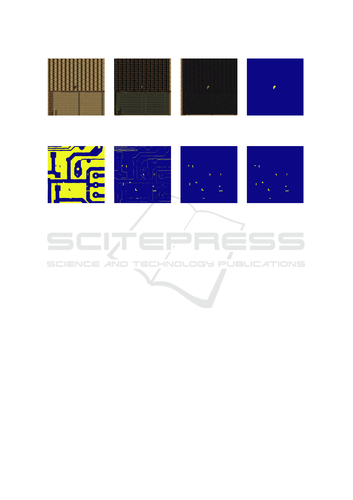
(a)
(b) (c) (d)
Figure 1: Our internal chip defect dataset: (a) sample, (b) difference image after SURF algorithm, (c) difference after the
DBSCAN of matching points, (d) binary label.
(a) (b) (c) (d)
Figure 2: DeepPCB dataset: (a) sample, (b) difference image after XOR operation (c) after mask operation, (d) final label.
thresholding between corresponding keypoint pixel
coordinates. Then the clustering algorithm DBSCAN
(Ester et al., 1996) removes the remaining outliers.
Finally, the translation is computed as the mean of
coordinate differences between matched keypoints.
Similar to (Chaudhary et al., 2017) and (Huang and
Wei, 2019) we compute the absolute difference be-
tween sample and template image. A median filter
with kernel size 5 removes single pixel errors. After
a normalization, more noise is removed by percentile
thresholding on pixel intensity. Finally we use a mor-
phology closing operation followed by a opening op-
eration with a 3×3 structuring element (see Figure 1)
to clean up results.
The image samples and templates of the deep-
PCB dataset are already aligned. Examination of the
dataset revealed that the alignment is sometimes non-
optimal. By sliding the template image in a small
pixel range over the sample and comparing the mean
square error between both, a better alignment could
often be found. After that, a pixel wise XOR opera-
tion between sample and template yields the differ-
ence image. Due to non-perfect image registration
and binarization, a lot of edges are still visible (see
Figure 2 (b)). Hence, we set everything to zero out-
side of the annotated bounding boxes. The remainder
of non-defect information was, like in the chip defect
dataset, removed with a closing operation, followed
by an opening operation (see Figure 2).
Data Augmentation. Data Augmentation is a com-
mon regularization technique to improve generaliza-
tion and to prevent overfitting due to lack of suffi-
cient amounts of data (Perez and Wang, 2017). In
the interest of finding models with good generaliza-
tion capabilities, as well as for real-world application,
augmentation transforms where selected to overcome
dataset shortcomings like positional biases and en-
courage models to generalize towards unseen testing
data. Therefore, every image is transformed with the
following 3 different geometric transformations: ro-
tation, cropping, and flipping (horizontal flipping and
vertical flipping). The most crucial point for data aug-
mentation is to preserve the correctness of the labels.
During training, the parameter for the transformations
are determined randomly and change for every epoch.
For the validation sets, 10 transformation parameter
sets were pre-determined for each test sample. Trans-
formations are always applied on the image sample
and the corresponding image label respectively.
3.2 Image Segmentation Models
In 2015, the U-Net CNN architecture, designed for
solving biomedical image segmentation tasks was in-
troduced (Ronneberger et al., 2015). The authors
claim that, sufficient data augmentation assumed,
dataset sizes can be small to achieve good results.
The feature maps of the contracting path (decoder)
are concatenated with the opposite feature maps of
U-Net based Zero-hour Defect Inspection of Electronic Components and Semiconductors
595
copy and concatenate
32
128x128
Conv 3x3 s=2
16
128x128
24
64x64
32
32x32
64 96
16x16
160 320 1280
8x8
Conv 1x1
320 96
16x16
48 48
32x32
24 24
64x64
1616
128x128
88
256x256
1
256x256
Sigmoid ac-
tivation
Inverted
residual block
Downsampling
unit
Transposed
Convolution
2x Convo-
lution 3x3
Figure 3: U-Net architecture with a MobileNetV2 x1.0 as the encoder. Numbers in x-axis direction are the channel numbers
in the output of a block, numbers in depth direction denote feature map resolutions.
the contracting path (encoder). That offers the advan-
tage that high resolution features from the contracting
path are combined with the up-sampled lower resolu-
tion features for precise localization.
Since we aim to run the U-Net on embedded
devices, it pays to consider specialized network ar-
chitectures. With the MobileNet, a new family of
efficient models, designed for mobile and embed-
ded applications was presented in 2017 (Howard
et al., 2017). This is achieved by replacing conven-
tional convolution operations with separable depth-
wise convolutions which reduce computational cost
about 8 to 9 times while maintaining accuracy for the
most part. An updated version was introduced with
the MobileNetV2 (Sandler et al., 2018). Here, the
main block of separable depthwise convolutions was
improved by adding a linear bottleneck layer and skip
connections between the bottleneck layers. To utilize
the efficiency of the MobileNetV2, the encoder path
of the U-Net is replaced with the former which yields
a network as it can be seen in Figure 3.
Shortly after the MobileNet, the ShuffleNet was
presented (Zhang et al., 2017). Similar to the Mo-
bileNetV2, the authors proposed a residual block
structure with bottleneck. Here the pointwise convo-
lutions are replaced by pointwise group convolutions
which are then followed by a channel shuffle opera-
tion. Again, a further improved version with the Shuf-
fleNetV2 (Ma et al., 2018) was introduced in 2018.
ShuffleNetV2 is also used as a replacement for the
original U-Net encoder.
3.3 Evaluation and Defect Detection
For evaluation of the different models, the Jaccard in-
dex also known as Intersection over Union (IoU) is
used. It is a similarity measure for finite sets and is
defined as the intersection of two sets divided by the
union of those sets:
J(A, B) =
|A ∩ B|
|A ∪ B|
=
|A ∩ B|
|A| + |B| − |A ∩ B|
(1)
where A and B are the two finite sets and 0 ≤
J(A, B) ≤ 1 is valid. The IoU metric computes the
amount of positive (defective) pixels common be-
tween the label and the predicted output and divides it
by the total amount of positive pixels present in both
images. The samples of the chip defect dataset with
no defects present can therefore not be used for eval-
uation. The IoU is averaged over all testset samples
as mean Intersection over Union (mIoU).
The basis for computing the IoU are binary out-
put images. With a sigmoid activation function in the
output layer, pixel intensities correspond to probabili-
ties for the positive class membership. By applying
a threshold, these probabilities can be converted to
binary pixel values which enables the usage of the
above mentioned metric. An optimal threshold of 0.3
was found by calculating the intersection over union
for an interval of thresholds.
While IoU is a reasonable metric for evaluating
model capabilities in image segmentation, one fur-
ther step is needed for the actual anomaly and defect
detection. In case of the DeepPCB dataset, we have
choosen DBSCAN algorithm (Cheng, 1995) to clus-
ter all positive pixels in the output images by means
of their coordinates and to remove outliers.
VISAPP 2021 - 16th International Conference on Computer Vision Theory and Applications
596

Table 1: Comparison of several models over anomalous region segmentation performance (mIoU), number of parameters and
computational complexity.
Model
mIoU Parameters GFLOPS
DeepPCB Chip Defect Encoder Decoder Total Encoder Decoder Total
U-Net depth 5, 64 channels 0.80 0.75 18.84M 12.19M 31.03M 13.06 23.97 36.93
U-Net depth 5, 16 channels 0.60 0.69 1.18M 0.76M 1.94M 0.84 1.50 2.34
MobileNetV2 x1.0 Encoder 0.70 0.73 2.22M 2.19M 4.41M 0.32 0.43 0.75
MobileNetV2 x0.5 Encoder 0.59 0.58 0.69M 0.96M 1.65M 0.10 0.19 0.29
ShuffleNetV2 x1.0 Encoder 0.74 0.68 1.25M 4.44M 5.69M 0.15 1.40 1.55
ShuffleNetV2 x0.5 Encoder 0.65 0.67 0.34M 1.24M 1.58M 0.043 0.56 0.61
Every found cluster is regarded as a defect. A
bounding box is computed such that all pixels which
are member of this cluster, lie inside the bounding
box. If the bounding box lies completely within the
bounding box of the defect, according to the anno-
tated ground truth data, the found cluster is regarded
as correctly classified (true positive or T P). If the
found cluster and its bounding box lies not completely
or not at all within an annotated bounding box, it is re-
garded as a false positive (FP). The difference of the
actual number of defects and found number of defects
(cluster) is the amount of false negatives (FN).
The same method could be applied to the semi-
conductor dataset. Since the samples of the dataset
show either no defect or exactly one defect, clustering
would be trivial. Therefore, a simple and alternative
classification method is used. All positively labeled
pixels in the output image are counted and if this value
is higher than a empirically found threshold, the sam-
ple is regarded as a defective one. The result then can
be compared with the ground truth for evaluation. In
addition to precision and recall, accuracy values can
be computed.
To compare the computational cost of the mod-
els, Floating Point Operations (FLOPs) are com-
puted as well as the numbers of trainable parame-
ters. These values help quantify possible efficiency
improvements through utilization of specialized Mo-
bileNetV2 and ShuffleNetV2 architectures.
3.4 Training Details
The datasets are split into fractions of 80% for train-
ing and 20% for validation. A test set is not used due
to the relatively small dataset sizes. mIoU values are
obtained by training the models with the k-fold cross
validation method. The 5 folds are stratified.
All input images are resized to 256 × 256 pix-
els before training. Image samples of the chip de-
fect dataset are normalized before training with µ =
[0.485, 0.456, 0.406] and σ = [0.229, 0.224, 0.225] for
the respective color channels. These values originate
from the ImageNet dataset. Additionally, random
data augmentations is applied. An Adam optimizer is
used with the default parameter values β
1
= 0.9 and
β
2
= 0.999 for the momentum decay rates and a learn-
ing rate of α = 0.0001. As we face a binary pixel-wise
classification task, we use BCE loss:
BCE = −y
p
log ˆy
p
− (1 − y
p
) log(1 − ˆy
p
) (2)
Here, y
p
is the probability of a output pixel belonging
to the positive class and ˆy
p
the ground truth label for
it.
All models are trained for 200 epochs with a batch
size of 16 samples per mini-batch.
We have implemented the CNN models with Py-
Torch. The Hardware used for training has a GeForce
GTX 1080 Ti GPU. For preprocessing of the data, the
open computer vision library OpenCV was used.
4 EXPERIMENTS
4.1 Datasets
All models were trained and evaluated on the publicly
available DeepPCB dataset (Tang et al., 2019) and an
internal semiconductor production line dataset.
The DeepPCB dataset contains 1500 grayscale
image samples with a resolution of 640 × 640 pixels.
Every image shows details and parts of bare PCBs,
including around 3 to 12 defects of common defect
types of PCBs. The amount of defects present in
each image was artificially increased. The samples
are paired with corresponding template images which
show the same PCB detail, but without any visual de-
fects. Samples and templates were aligned through
image registration techniques. All images are bina-
rized through a manually selected intensity threshold.
An annotation file is provided for every image sample
which contains the coordinates of axis aligned bound-
ing boxes for every defect visible in the image, as well
as the types of the occurring defects.
The semiconductor dataset contains 1474 color
image samples with a resolution of 600 × 600 pixels.
U-Net based Zero-hour Defect Inspection of Electronic Components and Semiconductors
597
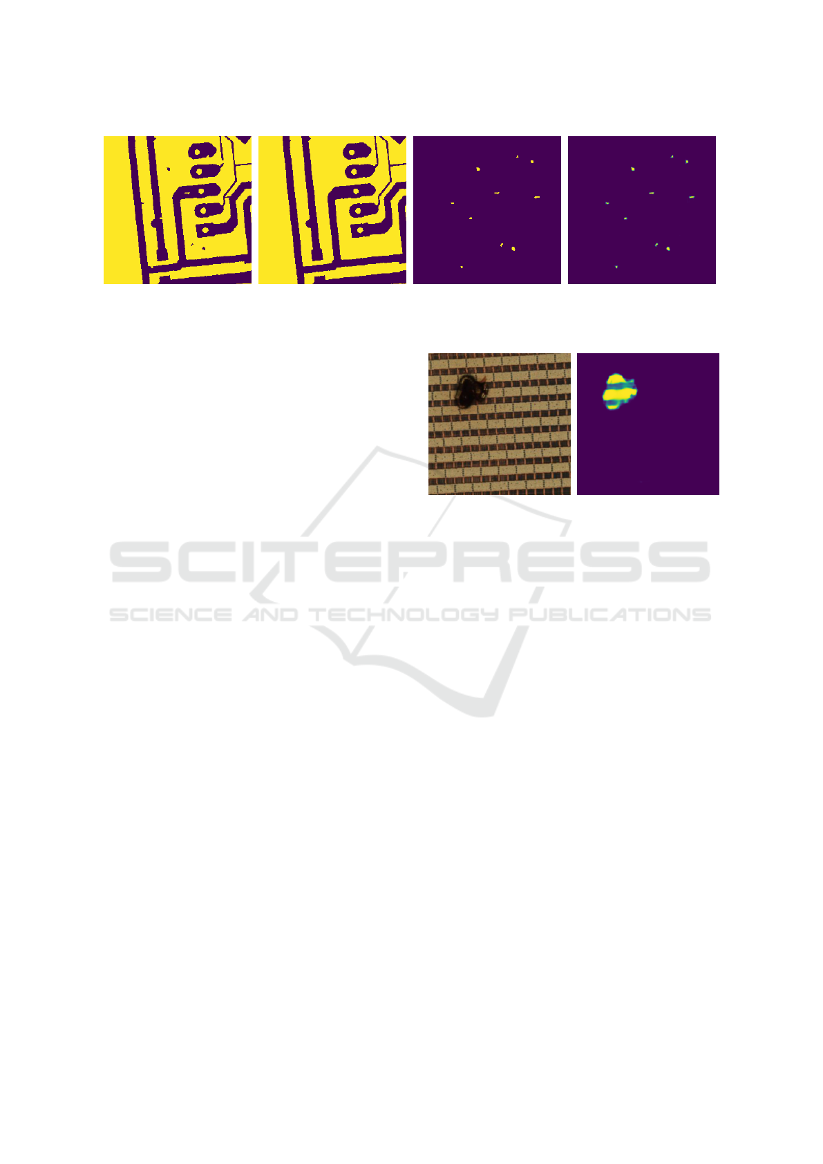
(a) (b) (c) (d)
Figure 4: Visualization of recognition for chip defect dataset: Input sample (a), template image (b), ground truth label (c) and
network output (d).
903 samples have no visual defect, the remaining 571
images contain exactly one visual defect close to the
image center. Every defect sample is classified as one
out of six types of common defects. For every sam-
ple, a corresponding and defect free template image
is available.
4.2 Baseline Results
First we establish whether a U-Net architecture can
learn the binary image segmentation task of divid-
ing the PCB and chip data samples into anomalous
and non-anomalous regions. The mean IoU for a U-
Net with default parameters, calculated over the test
sets, is 0.80 for the DeepPCB dataset and 0.75 for the
chip defect dataset (see Table 1 first row). The de-
fault parameters are a width of 64 channels in the first
stage and a model depth of 5 stages (equals four 2x2
max pool operations). These high IoU values can be
further confirmed by an visual inspection of example
outputs.
For the chip defect dataset, an output can be seen
in Figure 5 in (b). In the example, the network recog-
nizes the continuation of the horizontal pattern inside
the defect, but at the same time assumes an anomaly at
this position. That results in medium confident pixel
values which appear greenish. In Figure 4 (d) an out-
put of the DeepPCB dataset is depicted. The model
recovered all of the 10 small defects, when compared
with the ground truth label. Defect recovery seems
independent from whether the defects are pixels with
high values in regions of zero valued pixels or zero
values, surrounded by high value regions.
4.3 Ablation Study
Pretraining. In (Erhan et al., 2009) and (Yosinski
et al., 2014) it has been shown that using pre-trained
weights for DNNs in general improves optimization
and generalization. In (Iglovikov and Shvets, 2018)
it has been shown that using a VGG11 Encoder with,
(a)
(b)
Figure 5: Visualization of recognition for chip defect
dataset: Input sample (a) and network output (b).
previously on ImageNet pretrained weights, improves
image segmentation results. The same basic architec-
ture with the same pretrained encoder has been tested
both on the PCB and the semiconductor datasets.
Grayscale images were expanded from one channel
to three channels by copying the values to the two
added channels. For both datasets, mIoU over train-
ing epochs has been evaluated.
We find a 5 to 10% gap between mIoU values
when comparing training with and without the trans-
fer learning (Figure 6). The results here demon-
strate that pretraining improves results noticeably. As
a side effect, it additionally speeds up convergence.
Therefore, in the following experiments, all used Mo-
bileNetV2 and ShuffleNetV2 encoders are initialized
with ImageNet pretrained weights.
Resource Efficient Encoders. In this experiment,
U-Net models are tested where the original encoder
path is replaced by either a pretrained MobileNetV2
or a ShuffleNetV2. Results are average values of a
5-fold cross-validation. The best mIoU scores are
achieved by the MobileNetV2 encoder model with 0.7
and 0.73 mIoU respectively (see Table 1). The results
are close to the original U-Net model with 64 filters in
the first stage, with the mobileNetV2 being a far more
lightweight model. Note that for the MobileNetV2
VISAPP 2021 - 16th International Conference on Computer Vision Theory and Applications
598
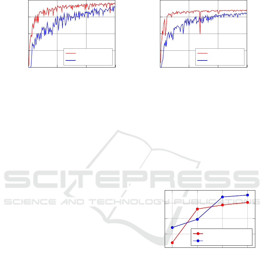
0
50
100
150
0
0.2
0.4
0.6
0.8
Epochs
Intersection over Union
pretrained
not pretrained
(a) DeepPCB dataset
0
50
100
150
0
0.2
0.4
0.6
0.8
Epochs
Intersection over Union
pretrained
not pretrained
(b) Chip defect dataset
Figure 6: mIoU for both datasets, plotted over training epochs. The pretrained model converges faster and shows better results.
x0.5, no pretrained models were available which ex-
plains lower scores in comparison to the other mod-
els. The ShuffleNetV2 x1.0 can report similar mIoU
scores with 0.74 but also a lower 0.65 for the chip
defect dataset. The reduced x0.5 version can almost
keep up with the x1.0 version with scores of 0.65 and
0.67.
ShuffleNetV2 is a newer architecture than Mo-
bileNetV2 and therefore a better performance might
be expected. As shown in (Ma et al., 2018), in
direct comparison with ShuffleNetV2 x1.0 the Mo-
bileNetV2 x1.0 has a slightly lower Top-1 classifica-
tion error on ImageNet. The results in this experiment
support this finding. On its own, the ShuffleNetV2 is
the lighter model but integrated in our U-Net model
the advantage is lost due to higher channel numbers
in the decoder when compared to the MobileNetV2.
In all instances, the computational complexity of
models with replaced encoder is a lot smaller than a
similar sized U-Net as can be seen in Table 1. No-
ticeable is that in the encoder paths, the parameter
counts are higher while the FLOP counts are lower.
The reason for that is that the parameters of the bot-
tleneck stage are making up almost 50% of the models
total parameter count and are counted to the encoder
path. At the same time, the transposed convolutions in
the decoder require much more FLOPs than the max
pooling operations of the encoder.
Influence of Available Training Data. The amount
of training data is crucial for the training success of
every deep neural network. To test the influence of
the available amount of training data on our image
segmentation models, a model has been trained re-
peatedly while the size of the training set was reduced
in steps of 20% of the complete dataset. At the same
time, the number of epochs have been increased such
that the number of iterations are kept equal. This
can give insights at which point data augmentation
is not able to compensate the lack of training data
any more. The tested model is the U-Net with Mo-
bileNetV2 x1.0 encoder.
The results, which are shown in Figure 7, suggest
that on the one hand, more training data could further
slightly improve results than the ones achieved here,
on the other hand, the actual available training data of
80% of the dataset seems to be sufficient since reduc-
ing the training set size step by step does not result in
an instant performance drop with 60% training data
still performing well in comparison.
20 40
60
80
0.5
0.6
0.7
Trainingset/Dataset (%)
Mean IoU
DeepPCB dataset
Chip defect dataset
Figure 7: U-Net with MobileNetV2 x1.0 encoder is trained
with reduced amounts of training data. Below 60% of the
complete dataset, the results decrease significantly.
4.4 Defect Detection
Since the two datasets are very different in nature, we
test two different but computationally cheap methods
for defect detection.
For the deepPCB dataset, all positive pixels in ev-
ery binary output image of the test set are clustered
with the DBSCAN algorithm. Parameters for the DB-
SCAN are minPts = 2 and ε = 2 . For every found
cluster, a bounding box is computed and is then com-
pared with a mask of annotated ground truth bounding
U-Net based Zero-hour Defect Inspection of Electronic Components and Semiconductors
599
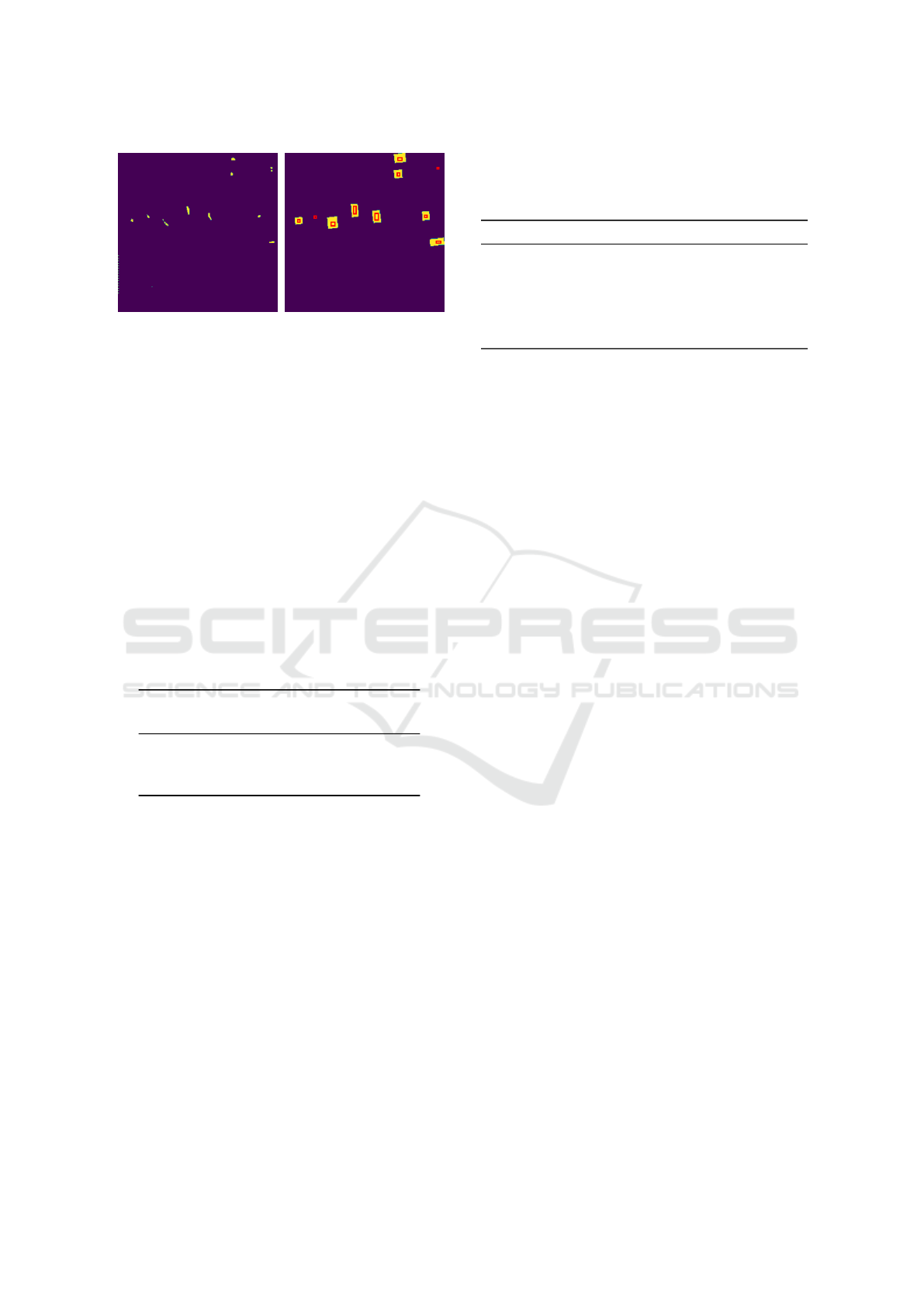
(a) (b)
Figure 8: Positive pixels of the binary output mask (a) are
clusterd with DBSCAN. Bounding boxes (red rectangles)
are computed of the found clusters. They are then com-
pared with the bounding boxes of the ground truth (yellow
rectangles) for classification (b).
boxes for classification, which is shown in Figure 8
(b) as an example. The test set contains 19610 defects
in total from which the ShuffleNetV2 x0.5 U-Net was
able to find and classify 19040 (97.1%) defects cor-
rectly (TPs) while the MobileNetV2 x1.0 U-Net man-
aged to detect 18919 (96.5%) defects correctly. Since
the number of FPs is less then half the number of
FPs of the ShuffleNet, the precision value for the Mo-
bileNetV2 is much higher with 0.963 when compared
to 0.915. The ShuffleNet misses 570 less defects (FN)
which leads to a slightly higher recall rate of 0.971.
Evaluation metrics can be seen in Table 2.
Table 2: Defect detection results deepPCB dataset.
ShuffeNetV2 MobileNetV2
x0.5 Encoder x1.0 Encoder
Precision 0.915 0.963
Recall 0.971 0.965
F1-Score 0.942 0.964
Since the samples of the chip defect dataset con-
tain either one defect or no defect, applying a sim-
ple threshold over the accumulated number of posi-
tive (defect) pixels in the binary output is tested for
two-class classification. The threshold is 70 pixels
and has been chosen in favour of small FP num-
bers. Several classification CNNs have been trained
on the chip defect dataset and the results are com-
pared to image segmentation U-Nets with different
encoders (see Table 3). All of the models achieved
high accuracy values between 98.2% and 99.0%, only
the original ShuffleNetV2 is somewhat behind with
93.4%. The lightweight MobileNetV2 performs bet-
ter than the more complex and deeper AlexNet and
wide ResNet models. The emphasize in this exper-
iment is still on the defects. Thus again precision
and recall scores are computed where the segmenta-
Table 3: Defect classification results of the chip defect
dataset are compared between CNN classification models
and U-Net based image segmentation models. On output
images of the latter, a threshold is applied for classification.
Network Acc.(%) Prec. Recall F1-score
AlexNet 98.2 0.967 0.988 0.977
ResNet-101 98.3 0.988 0.967 0.977
MobileNetV2x0.5 99.0 0.990 0.985 0.987
ShuffleNetV2x0.5 93.4 0.911 0.918 0.914
UNet/MNetV2x1.0 99.0 0.996 0.977 0.986
UNet/SNetV2x0.5 98.4 0.997 0.960 0.978
tion models have slightly higher precision scores with
0.997 as the highest for the ShuffleNetV2 x0.5.
Our approach shows equal or better results to the
more direct way of handling the task purely as a two
class classification problem. Additionally it supports
precise defect localization. Since the image segmen-
tation models delivering accurate results, only simple
post processing is necessary to extract the information
about existence and position of defects.
5 CONCLUSION
We presented a novel approach for visual inspection
and defect detection of PCBs and microchips. It tack-
les the task by regarding it as a binary image segmen-
tation problem where each pixel is classified individ-
ually to determine anomalous and defective regions
in the image. For this purpose, image segmentation
models were used, based on the fully convolutional U-
Net architecture. The proposed approach shows over-
all good and promising performance in the presented
experiments. With relatively simple post-processing
steps, the segmented image outputs can be utilized to
detect individual defects and localize them on the test
sample accurately. The optimization with specialized
MobileNetV2 and ShuffleNetV2 architectures in the
U-Net encoder path reduced network complexity sig-
nificantly. This clears the way for an integration on
embedded devices and therefore edge applications in
real-time. In comparison to most referential methods,
the approach of this work depends on reference im-
ages only for training, but not for inference of new
and unseen samples. Therefore, its biggest strength
lies in the obtained flexibility. For example an em-
bedded smart visual inspection system, consisting of
a camera and the defect detection model, can be set
up on arbitrary positions of the PCB manufacturing
process and can quickly react to design and process
changes without needing a new batch of reference im-
ages for small changes.
VISAPP 2021 - 16th International Conference on Computer Vision Theory and Applications
600

REFERENCES
Badrinarayanan, V., Kendall, A., and Cipolla, R. (2017).
Segnet: A deep convolutional encoder-decoder ar-
chitecture for image segmentation. IEEE Transac-
tions on Pattern Analysis and Machine Intelligence,
39(12):2481–2495.
Bay, H., Tuytelaars, T., and Van Gool, L. (2006). Surf:
Speeded up robust features. In Leonardis, A., Bischof,
H., and Pinz, A., editors, Computer Vision – ECCV
2006, pages 404–417, Berlin, Heidelberg. Springer
Berlin Heidelberg.
Chaudhary, V., Dave, I., and Upla, K. (2017). Automatic vi-
sual inspection of printed circuit board for defect de-
tection and classification. pages 732–737.
Chen, L., Papandreou, G., Schroff, F., and Adam, H.
(2017). Rethinking atrous convolution for semantic
image segmentation. CoRR, abs/1706.05587.
Chen, L.-C., Papandreou, G., Kokkinos, I., Murphy, K., and
Yuille, A. L. (2014). Semantic image segmentation
with deep convolutional nets and fully connected crfs.
arXiv preprint arXiv:1412.7062.
Cheng, Y. (1995). Mean shift, mode seeking, and clus-
tering. IEEE Trans. Pattern Anal. Mach. Intell.,
17(8):790–799.
d. S. Silva, L. H., d. A. Azevedo, G. O., Fernandes, B. J. T.,
Bezerra, B. L. D., Lima, E. B., and Oliveira, S. C.
(2019). Automatic optical inspection for defective pcb
detection using transfer learning. In 2019 IEEE Latin
American Conference on Computational Intelligence
(LA-CCI), pages 1–6.
Erhan, D., Manzagol, P.-A., Bengio, Y., Bengio, S., and
Vincent, P. (2009). The difficulty of training deep ar-
chitectures and the effect of unsupervised pre-training.
Journal of Machine Learning Research - Proceedings
Track, 5:153–160.
Ester, M., Kriegel, H.-P., Sander, J., and Xu, X. (1996).
A density-based algorithm for discovering clusters in
large spatial databases with noise. pages 226–231.
AAAI Press.
Howard, A. G., Zhu, M., Chen, B., Kalenichenko, D.,
Wang, W., Weyand, T., Andreetto, M., and Adam,
H. (2017). Mobilenets: Efficient convolutional neu-
ral networks for mobile vision applications. CoRR,
abs/1704.04861.
Huang, W. and Wei, P. (2019). A pcb dataset for defects
detection and classification.
Ibrahim, Z. and Al-Attas, S. (2005). Wavelet-based
printed circuit board inspection algorithm. Integrated
Computer-Aided Engineering, 12:201–213.
Iglovikov, V. and Shvets, A. (2018). Ternausnet: U-net with
vgg11 encoder pre-trained on imagenet for image seg-
mentation.
Indera Putera, S. H. and Ibrahim, Z. (2010). Printed cir-
cuit board defect detection using mathematical mor-
phology and matlab image processing tools. In 2010
2nd International Conference on Education Technol-
ogy and Computer, volume 5, pages V5–359–V5–
363.
Khalilian, S., Hallaj, Y., Balouchestani, A., Karshenas, H.,
and Mohammadi, A. (2020). Pcb defect detection us-
ing denoising convolutional autoencoders. In 2020 In-
ternational Conference on Machine Vision and Image
Processing (MVIP), pages 1–5.
Long, J., Shelhamer, E., and Darrell, T. (2014). Fully
convolutional networks for semantic segmentation.
CoRR, abs/1411.4038.
Ma, N., Zhang, X., Zheng, H., and Sun, J. (2018). Shuf-
flenet V2: practical guidelines for efficient CNN ar-
chitecture design. CoRR, abs/1807.11164.
Otsu, N. (1979). A threshold selection method from gray-
level histograms. IEEE Transactions on Systems,
Man, and Cybernetics, 9(1):62–66.
Perez, L. and Wang, J. (2017). The effectiveness of data
augmentation in image classification using deep learn-
ing. CoRR, abs/1712.04621.
Ren, S., He, K., Girshick, R. B., and Sun, J. (2015). Faster
R-CNN: towards real-time object detection with re-
gion proposal networks. CoRR, abs/1506.01497.
Ronneberger, O., Fischer, P., and Brox, T. (2015). U-net:
Convolutional networks for biomedical image seg-
mentation. CoRR, abs/1505.04597.
Sandler, M., Howard, A. G., Zhu, M., Zhmoginov, A., and
Chen, L. (2018). Inverted residuals and linear bottle-
necks: Mobile networks for classification, detection
and segmentation. CoRR, abs/1801.04381.
Santoyo, J., Pedraza Ortega, J. C., Mej
´
ıa, L., and Santoyo,
A. (2007). Pcb inspection using image processing and
wavelet transform. volume 4827, pages 634–639.
Srimani, P. and Prathiba, V. (2016). Adaptive data mining
approach for pcb defect detection and classification.
Indian journal of science and technology, 9.
Tang, S., He, F., Huang, X., and Yang, J. (2019). Online
pcb defect detector on a new pcb defect dataset.
Vafeiadis, T., Dimitriou, N., Ioannidis, D., Wotherspoon, T.,
Tinker, G., and Tzovaras, D. (2018). A framework for
inspection of dies attachment on pcb utilizing machine
learning techniques. Journal of Management Analyt-
ics, 5:1–14.
Wei, P., Liu, C., Liu, M., Gao, Y., and Liu, H. (2018).
Cnn-based reference comparison method for classi-
fying bare pcb defects. The Journal of Engineering,
2018(16):1528–1533.
Yosinski, J., Clune, J., Bengio, Y., and Lipson, H. (2014).
How transferable are features in deep neural net-
works? CoRR, abs/1411.1792.
Zhang, L., Jin, Y., Yang, X., Li, X., Duan, X., Sun, Y., and
Liu, H. (2018). Convolutional neural network-based
multi-label classification of pcb defects. The Journal
of Engineering, 2018(16):1612–1616.
Zhang, X., Zhou, X., Lin, M., and Sun, J. (2017). Shuf-
flenet: An extremely efficient convolutional neural
network for mobile devices. CoRR, abs/1707.01083.
Zhao, H., Shi, J., Qi, X., Wang, X., and Jia, J. (2016). Pyra-
mid scene parsing network. CoRR, abs/1612.01105.
U-Net based Zero-hour Defect Inspection of Electronic Components and Semiconductors
601
