
Integrated 3D-Capacitors for Implantable Bradycardia Pacemakers:
Dielectric Integrity and
Local Electrical Characterizations using AFM
Rosine Coq Germanicus
1a
, Florent Lallemand
2
, Nicolas Normand
2
, Catherine Bunel
2
and
Ulrike Lüders
1b
1
Normandie Univ., Ensicaen, Unicaen, Cnrs, Crismat, UMR 6508, 14000 Caen, France
2
Murata, 14000 Caen, France
Keywords: Silicon Capacitor, Implantable Electronic, AFM, SCM, Dielectric, Pacemaker.
Abstract: A silicon 3D-array capacitor dedicated for an implantable bradycardia pacemaker is presented. The integrated
3D-shape of the capacitors are designed by fabricating a high ratio micropore array inside the silicon wafer.
This special shape enhances the developed surface of the dielectric layer, leading to high capacitance densities,
critical for the application in such a biomedical system. The process control, based on nano-characterizations
performed on an Atomic Force Microscopy, is deployed for the three major critical fabrication steps: the
dielectric conformity, the in-situ phosphorus-doped polycrystalline silicon pore filling and the uniformity of
the doping of the electrodes of the SIS capacitor. After the chemical revelation of the deposited dielectric
layer, the conformity of the layer and the effectiveness of the filling are proven by AFM topographies.
Moreover, the delineation of the electrode doping is examined with the electrical Scanning Capacitance Mode
by recording the spatial extension and the carrier concentration. Macroscopic characterisations of the
dielectric properties show the stability of the 3D-patterning silicon capacitors concerning the applied voltage
and the temperature. Finally, a high integration solution, where the 3D-capacitor are embedded and
sandwiched into a multilayer printed circuit board, is exposed by employing thin epoxy laminates prepreg
sheets.
1 INTRODUCTION
Implanted medical systems and connected healthcare
with small intelligent physiological sensors require
microelectronic components with high electrical
reliability, high stability and with very low leakage
current (Porter et al., 2008).
For the bradyarrhythmia treatment, over one
million pacemakers are implanted in the pectoral
region annually (Mond & Proclemer, 2011).
Conventional pacemakers consist of an extravascular
pulse generator and electrodes for the cardiac
myocardium connections. The microelectronic
system senses cardiac activity and generates
depolarizing pulses. Nowadays, even though leadless
pacemakers have been developed (Beurskens et al.,
2019; Lee et al., 2018), conventional system are still
the most appropriate for patients who require special
a
https://orcid.org/0000-0002-6698-4853
b
https://orcid.org/0000-0002-5766-8031
treatment such as the dual-chamber pacing. Despite
some device-related complications and the periodical
surgical replacement, the effectiveness of implantable
pacemakers has been well demonstrated, as a life-
long treatment to prevent sudden cardiac failure and
death (Joung, 2013; Beck et al., 2010). Today,
research and development to integrate high-density
microelectronic device with more reliability, are still
on-going.
With the goal to offer highly integrated
microelectronic die solutions, in microelectronic
industry, the third dimension inside the
semiconductor wafer is more and more used to design
and fabricate integrated devices. This trend is also
monitored for the design of devices dedicated for
biomedical applications such as cardiac implantable
electronic devices (CIED). Driven by the system
integration and miniaturization, among these devices,
Germanicus, R., Lallemand, F., Normand, N., Bunel, C. and Lüders, U.
Integrated 3D-Capacitors for Implantable Bradycardia Pacemakers: Dielectric Integrity and Local Electrical Characterizations using AFM.
DOI: 10.5220/0010254300490057
In Proceedings of the 14th International Joint Conference on Biomedical Engineering Systems and Technologies (BIOSTEC 2021) - Volume 1: BIODEVICES, pages 49-57
ISBN: 978-989-758-490-9
Copyright
c
2021 by SCITEPRESS – Science and Technology Publications, Lda. All rights reserved
49
highly integrated passive components, such as
inductors, resistors and capacitors are required. The
pacemaker, implanted to provide electrical
stimulation to the heart, needs amplifier circuits to
sense the cardiac activity and to filter signal
interferences (Busygina, 2019). In the
microelectronic sensing chain acquisition, the
capacitors act as an integrated electromagnetic
interference (EMI) filter and DC blocking
components (Haddad et al., 2006). These functions
are essential for the design of the microelectronic
chain. In this article, we present an integrated 3D-
silicon capacitor dedicated for an implantable
bradycardia pacemaker and we report nano-
characterizations of the dielectric layer and local
electrical measurements, performed on an Atomic
Force Microscopy (Vandervorst et al., 2017; Zhong
& Yan, 2015).
The integrated 3D-shape of the capacitors
enhances the developed surface of the dielectric layer
of the biomedical implanted Semiconductor-
Insulator-Semiconductor (SIS) system. Such a high
internal interface allows for high capacitance values,
although with a small footprint of the capacitor, ideal
for integration. A recent publication presents the state
of the art of integrated on-chip capacitors also called
microcapacitors (Hourdakis & Nassiopoulou, 2020).
2D and 3D patterning devices, reported in the
literature, are compared in terms of density and
electrical properties. The presented capacitors have
been integrated in a microporous silicon wafer to
reach the capacitance of 20 nF/mm², with a very low
leakage current, a high breakdown voltage and a high
reliability. However, the 3D structure leads to a
higher number of possible defect sources, due to its
complex structure. The deposition of the active layers
inside the pores has to be very well controlled in order
to ensure the conformity of the thickness of the layers
even at the bottom of the pores, and the absence of
clogging and resulting voids in the filling material, for
example. Therefore, highly controlled fabrication
processes are used, and adapted characterisation
techniques for these special aspects were developed.
In this contribution, we will present a detailed
study on different issues related to the use of 3D
structures. Using an Atomic Force Microscopy
(AFM), the integrity of the dielectric layer inside the
3D structures, i.e. the micrometric pores, is
investigated. Selective etching of a cross-section
sample allows for the direct observation of the
thickness of the dielectric layer along the pore edge.
The same method is also employed to characterize the
poly-silicon filling of the pores. In addition, AFM
nano-electrical analysis is deployed to map the active
dopant distribution of the semiconductor, especially
important for the here used geometry of the electrical
contacts, where both top and bottom electrode have to
be accessible on the surface of the die in order to
allow for its integration into the pacemaker circuits.
Macroscopic electrical characterizations (current –
voltage, capacitance – voltage and capacitance –
temperature) of the integrated device are also
presented, confirming the high stability of the
dielectric performances of these capacitors. Finally, a
possible solution of an advanced integrated
packaging of the passive devices in a CIED is
developed.
2 EXPERIMENTAL DETAILS
2.1 SIS Capacitor Fabrication Process
In the fabrication process, passive components such
as high-Q inductors, isolation diodes and accurate
resistors, are co-integrated with high-density SIS
capacitors inside the biomedical devices. In order to
obtain a high capacitance per surface area, a three-
dimensional structuring of the silicon wafer was
chosen (Brunet & Kleimann, 2013; Murray et al.,
2007; Roozeboom et al., 2006).
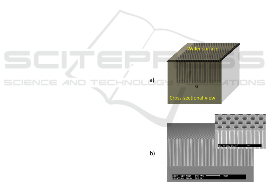
Figure 1: Silicon wafer after the etching of micropores
inside the substrate, a) top-view and cross-sectional optical
images of the wafer and b) cross-sectional SEM
observations before filling.
The starting material is a p-type (boron doped)
highly ohmic (1kΩ.cm) (001)-oriented single crystal
silicon wafer, with a thickness of 675 µm. To
fabricate the highly integrated capacitor, an array of
BIODEVICES 2021 - 14th International Conference on Biomedical Electronics and Devices
50
micropores is created inside the silicon substrate by
reactive ion etching (RIE) with a high aspect ratio
around 20. The so-called Bosch process is used, with
alternating steps of SF
6
/O
2
plasma etching and
passivation to dig into the silicon wafer (Gomez et al.,
2004). The goal of the process is to increase the
device density and multiply of the effective surface of
the capacitance.
Figure 1.a) and b) show optical views of the
silicon substrate surface after the RIE process, where
the shape of the RIE etched micropores array can be
observed. In Figure 1.b), cross-sectional SEM
observations of the same pores are presented. The
hole diameter is 1 µm, with a distance 1 µm between
the trench holes for a depth of 17 µm. Therefore, the
effective capacitor surface of the device is increased
by the circular trench holes inside the semiconductor.
In order to assure high reliability (high breakdown
voltage and lower failure rates) a multilayer dielectric
are designed (Kobayashi et al., 1990; Spitzer &
Baunach, 1989). The triple layered dielectric consists
of an Oxide-Nitride-Oxide (ONO) stack. After the
etching step, the ONO stack is deposited inside the
pore array. The first oxide layer (10 nm) is created by
thermal processing in dry O
2
. The nitride layer is a
LPCVD (low pressure chemical vapor deposition)
nitride from SiH
2
Cl
2
and NH
3
. The thickness of the
sandwiched nitride layer is 13 nm. The last deposited
layer is a thin oxide deposited by LPCVD from
tetraethylorthosilicate (TEOS) for the second oxide,
with a thickness of 12 nm.
Finally, a doped poly-silicon layer is deposited
inside the pores as top electrode by PECVD (Plasma
enhanced chemical vapour deposition) from SiH
4
and
PH
3
.
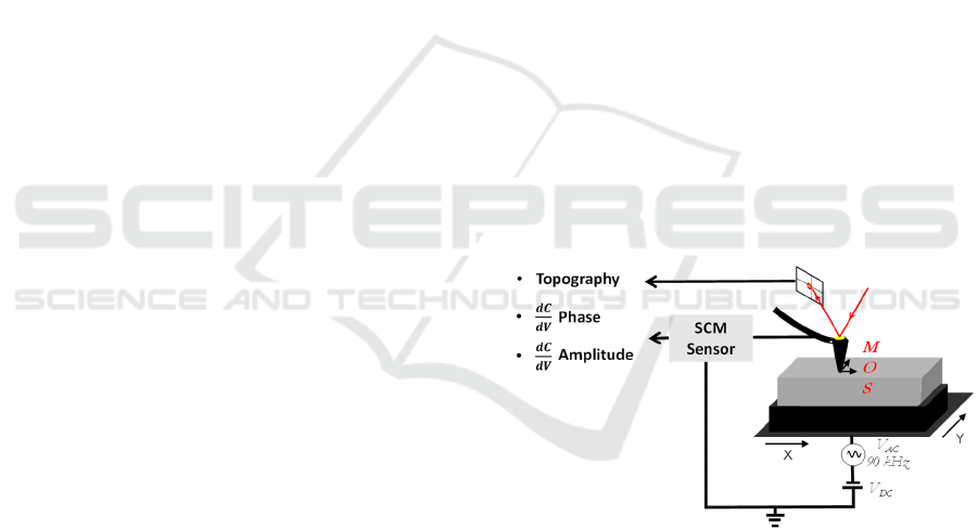
2.2 AFM Characterizations
AFM characterizations are performed on a
Dimension Icon Atomic Force Microscope by
Bruker. Measurements were done at room
temperature. Experiments presented here were
performed on carefully prepared cross-sections: after
cleaving the wafer, successive polishing steps were
carried out, in order to obtain a very smooth surface
to be analyzed.
Two AFM modes were deployed to analyse the
integrated capacitor. First, the Peak-Force Tapping
mode is used to acquire the topography of the cross-
section. With this mode, the conformity of the
dielectric layer will be demonstrated. A silicon nitride
AFM tip with a radius of 2 nm and a spring constant
of 0.4 N/m was used to map the surface of the sample.
The frequency of the cantilever is 70 kHz.
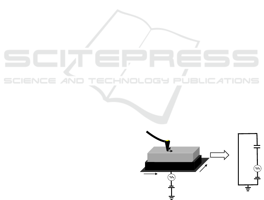
Second, the electrical Scanning Capacitance
microscopy (SCM) (De Wolf et al., 2001; Mody &
Nxumalo, 2019) mode was employed in order to
localize the active dopants of the integrated 3D-
capacitors. For this mode, a Platinum-Iridium coated,
electrically conductive tip probes the surface, allows
to unveil the local electrical properties of the silicon.
The conductive tip, in contact with the sample, plays
the role of the metal electrode in a nanometric Metal-
Oxide-Semiconductor (MOS) structure (Figure 2.a).
The necessary oxide layer on the cross-section is
created by an annealing step at 270 °C during 30 min
in air, resulting in a high-quality surface with constant
thickness. A constant (DC) bias voltage is applied
between the tip and the sample during the contact,
while a simultaneously applied low frequency AC
voltage modulates the local capacitance. With the
SCM sensor, the measurement of the local differential
capacitance allows to extract a 2D-map of the active
dopants of the semiconductor. The variation of this
nano-MOS capacitance is detected and measured
with a highly sensitive capacitance sensor, as small as
10
-19
F/(Hz)
1/2
. At each pixel, the capacitance
variations ( ∂ C/ ∂ V) depend on the charge
concentration of the majority carriers and therefore,
the local active doping concentration.
In order to minimize the influence of the AFM
laser light, the laser beam was not focused on the tip
edge but on the cantilever. Moreover, an anti-
vibration table was used to eliminate any ground
vibrations and/or acoustic noise. The AFM image
resolution was 512 × 512 points.
Figure 2: Schematic of the SCM mode based on an AFM,
topography and local capacitance variation on the nano-
MOS (the conductive tip in contact with the semiconductor)
in phase and amplitude, simultaneously.
3 RESULTS
3.1 Conformity of the Dielectric Layer
and Polycrystalline Silicon Filling
The reliability of the integrated SIS capacitor is
directly related to the nature, quality, thickness
control and conformity of the dielectric layer in the
Integrated 3D-Capacitors for Implantable Bradycardia Pacemakers: Dielectric Integrity and Local Electrical Characterizations using AFM
51
high aspect ratio structure (Jacqueline et al., 2013).
The crucial point is the conformal filling of the
bottom of the micropores. First, the deposition being
done from the top of the pores, the pore bottom will
be the most vulnerable position in case of a non-
perfect deposition of the layers. Second, from an
electrical point of view, the capacitor has in this area
a curvature of the electrodes, and therefore a locally
enhanced electrical field. Conformity problems of the
dielectric layer in this part of the pore will therefore
have a strong effect on the leakage currents and the
breakdown of the capacitor. Thus, a special attention
should be paid to the conformity in this area of the
capacitor.
Figure 3.a) represents the AFM topography of the
bottom of the pores after dielectric deposition. In
order to analyse the dielectric layer, we performed a
plasma etching with a high selectivity of silicon
compared to the nitride and the oxide. In Figure 3.b),
the surface topography after the plasma etching is
presented. The dielectric layer can be clearly
identified as the areas with a larger height compared
to the Si wafer and the poly-Si pore filling. The
selective etching therefore reveals the dielectric layer,
and its thickness conformity down to the bottom parts
of the pores is clearly visible in the topography
measurement. A close-up of the interesting area is
shown in Figure 3 b) and c), after the filling of the
pores, i.e. in the final device.
Figure 3: AFM topography measurements of the dielectric
layers in the 3D structures 5 µm × 5 µm, a) as-prepared, b)
after plasma etching to reveal the dielectric layer, before
filling of the pores.
After the deposition of the dielectric, the
micropores are filled with an in-situ n-doped
polycrystalline silicon. The topography of the cross-
sectioned sample is shown in Figure 3 a). The
polycrystalline structure of the filling can be very
well acknowledged by the topographical contrast in
this area. The preparation of the cross-section by
cleaving and polishing has a different effect on the
different crystalline directions of the poly-Si filling,
leading to different heights for different grains.
Figure 4: a) Scan of 6 µm × 6 µm of the bottom of the SIS
capacitor after polysilicon filling, b) topography of 2µm ×
2 µm and c) zoom 500 nm × 500 nm.
Again, to highlight the dielectric layer, the cross-
sectioned sample is also plasma-etched. In Figure
4.a), the complete filling of the polysilicon layer,
without voids, is observed. The scan represented in
Figure 4.b) shows the polysilicon grains and the
mechanical robustness of the dielectric layer, at the
BIODEVICES 2021 - 14th International Conference on Biomedical Electronics and Devices
52
bottom of the pore. No deformation, delamination or
crack has been observed on the AFM acquisitions.
During deposition and thermal annealing, the wafer
can undergo high local mechanical stress, thus AFM
topographies prove the very high mechanical strength
of the thin dielectric layer.
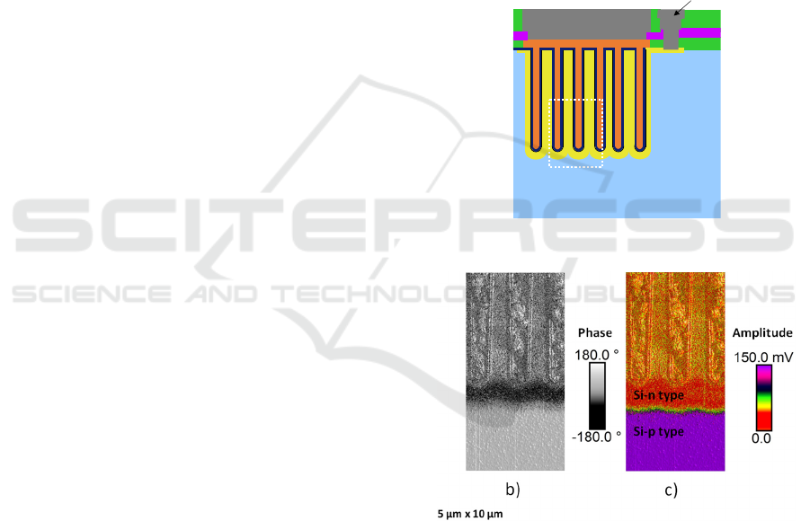
3.2 Local Electrical Measurement
based on an AFM
In order to facilitate the integration of the capacitors
in the pacemaker circuit, the contact to both the top
(the poly-Si filling) and the bottom electrode (the Si
wafer around the micropores) of the SIS capacitor are
designed and made with metallic contacts on the
surface of the die. This point is important because in
general, the backside of the silicon wafer is simply
doped to create the contact. But in the case of the
pacemaker circuit, a high degree of integration of the
passive is needed, so that the contacts to both top and
bottom electrodes must be accessible on the same
wafer side (Figure 5.a)). In order to reduce the
parasitic serial contact resistance and increase the
conduction of the bottom electrode, an n-type doping
implantation of the Si wafer in the pore areas is
carried out, followed by a thermal diffusion step. The
challenge of this step is to well define the bottom
electrode of the 3D-array SIS capacitors, i.e. to
achieve a highly doped Si zone along and at the
bottom of the pores with a spatial extension allowing
for an efficient electrical contact to the pore
interstitials.
To characterize the effective dopant carrier
distribution in the 3D structure, the sample is
analysed with the SCM mode. For this mode a
dedicated conductive AFM tip is used. SCM
parameters, such the applied bias V
DC
and V
AC
were
optimized (Appendix). The results are presented in
Figure 5 b) and c). For this acquisition, the two
applied bias to the tip-surface system are V
AC
= 2 V
and V
DC
= 1 V. The map of the Figure 5.a) is the phase
of the capacitance change (∂C/∂V) recorded at each
pixel during the scan. The image contrast is due to the
variation of the dopant type (Appendix, Figure 11).
The p-type substrate has a light grey colour while the
implanted region is identified by a negative phase
signal in dark grey colour. With this analysis, it is
possible to characterize the effective depth of the
doped wafer areas, after implantation and diffusion
steps. As described, this local doping delimits the
conduction area of the bottom electrode of the
integrated capacitor. To reach electrical requirements
such as a very low electrical resistance, the implanted
and diffused high doping uniform must be very
uniform in the 3D-structure. As we can see, in Figure
5. c), the doping depth exceeds well the micropore
depth. From the analysis of the SCM profiles, the
effective doping extends to a depth of 1.3 µm from
the bottom of the structures. This parameter ensures a
very good conduction of the layer without possible
leakage.
This doping distribution is confirmed by the SCM
amplitude signal, with, in addition, the highlighting
of the Si P-N junction. Since the SCM amplitude is
related to the C-V dependence of the tip-sample nano-
MOS, the signal is inversely proportional to the
doping concentration. The high carrier concentration
in the implanted area at the bottom of the micropores
can be therefore observed very clearly.
Figure 5: SCM results, scan size: 5µm × 10µm a)
Schematics of the capacitor structure, with top and bottom
electrodes on the same wafer side. b) SCM phase signal and
c) SCM amplitude cartography of the area marked by a
rectangle in a).
3.3 Global Electrical Characterizations
of the SIS Capacitor
In medical applications, the stability of CIED
including the passive devices is extremely important.
Being implanted, a failure of the devices may not only
have a heavy impact on the health of the patient, but
Si
3D- Capa SIS
Contact
Contact
a)
Integrated 3D-Capacitors for Implantable Bradycardia Pacemakers: Dielectric Integrity and Local Electrical Characterizations using AFM
53
may also generate important risks for their
replacement. The different parts have to have a stable
and predictable output for the signal treatment, and
this on long timescales.
Figure 6 shows the typical current-voltage of the
3D-Capacitor array, up to 28 V. Three distinct
transport mechanisms govern the conduction
mechanism in the SIS structure: the Poole-Frenkel
conduction, the Fowler–Nordheim tunneling of
carriers and the hot carrier injection (Palumbo et al.,
2020; Spitzer & Baunach, 1989). A breakdown
voltage of around 23 V is measured for the designed
3D SIS.
Moreover, the leakage current represents also a
key parameter for microelectronic reliability of
CIED. For the integrated SIS silicon capacitors, in an
implantable pacemaker, the nominal supply voltages
are up to 3.5 V and for this range the leakage current
remains below 0.5 nA for 25 nF/mm². We can note
that the capacitors are qualified for voltages up to 7 V.
Figure 6: Current – Voltage characteristics of the 3D
capacitor. The inset shows the same data in a logarithmic
scale.
Therefore, the output capacitance of the here
investigated 3D capacitances has been characterized
as a function of voltage and temperature. Figure 7
shows the capacitance as a function of the voltage for
the 3D-SIS capacitor. For small and positive voltages,
the capacitance is in the so-called accumulation
regime, leading to a stable output capacitance. Only
for negative voltages, where the capacitor enters the
depletion regime, the output capacitance decreases.
However, this decrease corresponds to only 0.8 % for
the highest applied voltage of -6 V, illustrating the
wide range of stability of the capacitor.
Figure 7: Capacitance variation of the SIS capacitor as a
function of the applied voltage, C
0
= 25 nF/mm².
Dedicated for biomedical applications, the
temperature of the environment may also vary,
although these variations are rather small. In order to
investigate the stability on the typical human body
temperature range, the variation of the capacitance in
the temperature range from -50 °C to 125 °C is
evaluated (Figure 8). For the full temperature range,
the evolution of the capacitance is observed to be 3
per mille per °C, which is a largely satisfactory value
for the use in pacemakers.
Figure 8: Capacitance variation of the SIS capacitor as a
function of the temperature.
3.4 Device Integration into Printed
Circuit Board
Another important point to consider is the integration
issue of the chip in the circuit. Indeed, the thickness
reduction and integration of the component allows
controlling circuit space requirement. For that, the
processed silicon wafer is thinned for the device
assembly. The 3D-silicon capacitor offers the
possibility to be ultra-low profile and can be
embedded into the inner layers of the printed circuit
board. Consequently, comparing to the classical
surface-mounted substrates, embedded devices
0 5 10 15 20 25 30
0.0
4.0x10
-5
8.0x10
-5
1.2x10
-4
I(A)
V
To
p
-V
Bot
(V)
0 5 10 15 20 25 30
10
-12
10
-10
10
-8
10
-6
10
-4
Breakdown
-6-4-20246
0.992
0.994
0.996
0.998
1.000
1.002
1.004
C/C
0
V
To
p
-V
Bot
(V)
-80 -40 0 40 80 120
0.996
0.998
1.000
1.002
1
.
004
C/C
0
Temp (°C)
BIODEVICES 2021 - 14th International Conference on Biomedical Electronics and Devices
54
increase the integration density of the package. For
this packaging process we chose to use a FR4
substrate. The FR4, glass-reinforced epoxy laminate
prepreg material (Kugler et al., 2011), is used for its
low process temperature and its high mechanical
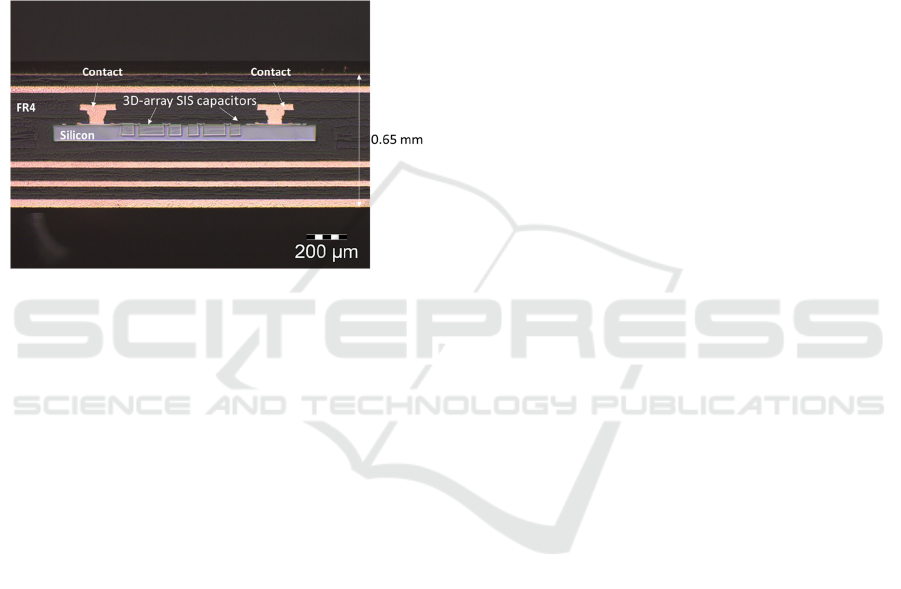
reliability. To illustrate the device integration
capability, Figure 9 shows the SIS capacitors
embedded into a FR4 material. Eight layers of FR4
are stacked together to obtain a total thickness of 0.65
mm. The interconnections (metallic contacts) of the
SIS capacitor chip are form with microvias. Then, a
multilayer package including the semiconductor is
fabricated.
Figure 9: SIS capacitors embedded into a FR4 packaging.
Another advantage to embed the die into the
printed circuit board is to reduce the parasitic
inductance between the compounds. In addition, with
this embedded technique, both active and passive
chips can be integrated in the same multilayer system.
This high integration solution also allows for the use
of the 3D-capacitors for the design of future
implantable, wearable and flexible circuits for
medical application.
4 CONCLUSIONS
The local and macroscopic electrical characteristics
of a 3D-integrated capacitor for implantable
bradycardia pacemaker applications were
investigated. The use of Atomic Force Microscopy
has allowed to highlight the conformity of the
deposited dielectric layer even in the bottom parts of
the pores, as well as the complete filling of the pores
with poly-Si. In addition, Scanning Capacitance
Microscopy was used to investigate the spatial
extension and the carrier concentration of the
differently doped zones in the structure. Furthermore,
macroscopic capacitance measurements show the
stability of these capacitors as a function of voltage
and temperature, making them ideal devices for the
use in biomedical applications. And even more, their
high reliability, especially compared to ceramic
technology, is an important asset for critical life
support applications. Finally, a highly integrated
solution into a printed circuit board is shown by
embedding the 3D-capacitors with laminate sheets.
This device configuration opens future fields of
application as future advances of implantable,
Internet of Medical Things (IMedT), Internet of
Things (IoT), as well as wearable and flexible circuits
for handheld diagnostic devices.
ACKNOWLEDGEMENTS
The authors would like to thank the Normandy region
and European Regional Development Fund through
the projects RIN RECHERCHE PLACENANO;
contract No. 18E01664/ 18P02478. This
investigation is supported also by the Carnot ESP
PACK5G program. The authors would like to thank
Christophe Pistis for the sample preparation.
REFERENCES
Beck, H., Boden, W. E., Patibandla, S., Kireyev, D., Gupta,
V., Campagna, F., Cain, M. E., & Marine, J. E. (2010).
50th Anniversary of the First Successful Permanent
Pacemaker Implantation in the United States :
Historical Review and Future Directions. The American
Journal of Cardiology, 106(6), 810‑818.
https://doi.org/10.1016/j.amjcard.2010.04.043
Beurskens, N. E. G., Breeman, K. T. N., Dasselaar, K. J.,
Meijer, A. C., Quast, A.-F. B. E., Tjong, F. V. Y., &
Knops, R. E. (2019). Leadless cardiac pacing systems :
Current status and future prospects. Expert
Review of Medical Devices, 16(11), 923‑930.
https://doi.org/10.1080/17434440.2019.1685870
Brunet, M., & Kleimann, P. (2013). High-Density 3-D
Capacitors for Power Systems On-Chip : Evaluation of
a Technology Based on Silicon Submicrometer Pore
Arrays Formed by Electrochemical Etching. IEEE
Transactions on Power Electronics, 28(9), 4440‑4448.
https://doi.org/10.1109/TPEL.2012.2233219
Busygina, A. V. (2019). Methods for Ensuring the
Sustainability of Pacemakers. 2019 International
Multi-Conference on Engineering, Computer and
Information Sciences (SIBIRCON), 0199‑0202.
https://doi.org/10.1109/SIBIRCON48586.2019.8958175
De Wolf, P., Brazel, E., & Erickson, A. (2001). Electrical
characterization of semiconductor materials and
devices using scanning probe microscopy. Materials
Science in Semiconductor Processing, 4(1), 71‑76.
https://doi.org/10.1016/S1369-8001(00)00174-8
Integrated 3D-Capacitors for Implantable Bradycardia Pacemakers: Dielectric Integrity and Local Electrical Characterizations using AFM
55
Gomez, S., Belen, R. J., Kiehlbauch, M., & Aydil, E. S.
(2004). Etching of high aspect ratio structures in Si
using SF6/O2 plasma. Journal of Vacuum Science &
Technology A: Vacuum, Surfaces, and Films, 22(3),
606. https://doi.org/10.1116/1.1710493
Haddad, S. A. P., Houben, R. P. M., & Serdijin, W. A.
(2006). The evolution of pacemakers. IEEE
Engineering in Medicine and Biology Magazine, 25(3),
38‑48. https://doi.org/10.1109/MEMB.2006.1636350
Hourdakis, E., & Nassiopoulou, A. G. (2020).
Microcapacitors for Energy Storage: General
Characteristics and Overview of Recent Progress.
Physica Status Solidi (a), 217(10), 1900950.
https://doi.org/10.1002/pssa.201900950
Jacqueline, S., Domengès, B., Voiron, F., & Murray, H.
(2013). Conduction mechanisms in 2D and 3D SIS
capacitors. Semiconductor Science and Technology,
28(4), 045018. https://doi.org/10.1088/0268-
1242/28/4/045018
Joung, Y.-H. (2013). Development of Implantable Medical
Devices : From an Engineering Perspective.
International Neurourology Journal, 17(3), 98‑106.
https://doi.org/10.5213/inj.2013.17.3.98
Kobayashi, K., Miyatake, H., Mitsuhashi, J., Hirayama, M.,
Higaki, T., & Abe, H. (1990). Dielectric breakdown and
current conduction of oxide/nitride/oxide multi-layer
structures. Digest of Technical Papers.1990
Symposium on VLSI Technology, 119‑120.
https://doi.org/10.1109/VLSIT.1990.111037
Kugler, A., Koyuncu, M., Zimmermann, A., & Kostelnik,
J. (2011). Chip Embedding in Laminates. In J.
Burghartz (Éd.), Ultra-thin Chip Technology
and Applications (p. 159‑165). Springer.
https://doi.org/10.1007/978-1-4419-7276-7_14
Lee, J. Z., Mulpuru, S. K., & Shen, W. K. (2018). Leadless
pacemaker : Performance and complications. Trends in
Cardiovascular Medicine, 28(2), 130‑141.
https://doi.org/10.1016/j.tcm.2017.08.001
Mody, J., & Nxumalo, J. (2019). Scanning Capacitance
Microscopy for Two-Dimensional Carrier Profiling of
Semiconductor Devices. In U. Celano (Éd.), Electrical
Atomic Force Microscopy for Nanoelectronics (p.
107‑142). Springer International Publishing.
https://doi.org/10.1007/978-3-030-15612-1_4
Mond, H. G., & Proclemer, A. (2011). The 11th world
survey of cardiac pacing and implantable cardioverter-
defibrillators : Calendar year 2009--a World Society of
Arrhythmia’s project. Pacing and Clinical
Electrophysiology: PACE, 34(8), 1013‑1027.
https://doi.org/10.1111/j.1540-8159.2011.03150.x
Murray, F., LeCornec, F., Bardy, S., Bunel, C., Verhoeven,
J. F. c, Heuvel, F. C. M. van den, Klootwijk, J. H., &
Roozeboom, F. (2007). Silicon Based System-in-
Package : A new technology platform supported by
very high quality passives and system level design
tools. 2007 Topical Meeting on Silicon Monolithic
Integrated Circuits in RF Systems, 149‑153.
https://doi.org/10.1109/SMIC.2007.322803
Palumbo, F., Wen, C., Lombardo, S., Pazos, S., Aguirre, F.,
Eizenberg, M., Hui, F., & Lanza, M. (2020). A Review
on Dielectric Breakdown in Thin Dielectrics : Silicon
Dioxide, High-k, and Layered Dielectrics. Advanced
Functional Materials, 30(18), 1900657.
https://doi.org/10.1002/adfm.201900657
Porter, M., Gerrish, P., Tyler, L., Murray, S., Mauriello, R.,
Soto, F., Phetteplace, G., & Hareland, S. (2008). Reliability
considerations for implantable medical ICs. 2008 IEEE
International Reliability Physics Symposium, 516‑523.
https://doi.org/10.1109/RELPHY.2008.4558939
Roozeboom, F., Kemmeren, A. L. A. M., Verhoeven, J. F.
C., van den Heuvel, F. C., Klootwijk, J., Kretschman,
H., Frič, T., van Grunsven, E. C. E., Bardy, S., Bunel,
C., Chevrie, D., LeCornec, F., Ledain, S., Murray, F.,
& Philippe, P. (2006). Passive and heterogeneous
integration towards a Si-based System-in-Package
concept. Thin Solid Films, 504(1), 391‑396.
https://doi.org/10.1016/j.tsf.2005.09.103
Spitzer, A., & Baunach, R. (1989). The physics of ONO layer
dielectrics. Applied Surface Science, 39(1), 192‑199.
https://doi.org/10.1016/0169-4332(89)90433-9
Vandervorst, W., Fleischmann, C., Bogdanowicz, J.,
Franquet, A., Celano, U., Paredis, K., & Budrevich, A.
(2017). Dopant, composition and carrier
profiling for 3D structures. Materials Science in
Semiconductor Processing, 62, 31‑48.
https://doi.org/10.1016/j.mssp.2016.10.029
Zhong, J., & Yan, J. (2015). Seeing is believing : Atomic
force microscopy imaging for nanomaterial
research. RSC Advances, 6(2), 1103‑1121.
https://doi.org/10.1039/C5RA22186B.
APPENDIX
In this section, SCM measurements and the
optimization of the parameters are described. In the
SCM mode, the local contact of the tip apex with the
sample forms a nano-MOS contact. During
measurements, two voltages V
DC
and V
AC
are applied
(Figure 10).
Figure 10: Scanning Capacitance measurement.
This mode allows to characterize majority carrier
concentrations and carrier types in semiconductors. In
fact, the electrically conductive tip is scanned in
V
AC
90 kHz
V
DC
M
O
S
Y
X
V
AC
90 kHz
V
DC
M
O
S
BIODEVICES 2021 - 14th International Conference on Biomedical Electronics and Devices
56

contact with the analysed sample surface. The nano-
contact, between the tip and probed local sample
volume, represents a nanometric Metal-Insulator-
Semiconductor (MIS) structure. A V
AC
signal is
superimposed to the applied V
DC
in order to record
the derivative local capacitance under the tip. The low
frequency of the AC voltage is typically around 100
kHz. The role of this voltage is to generate the
movement of free carriers in the material under the
probe contact. The capacitance variation is measured
with a highly sensitive capacitance sensor with
sensitivity around 10
-19
F/(Hz)
1/2
.
In order to well distinguish the active dopant the
V
DC
during measurement must be located at the value
where the slope of the C-V is maximum. Figure 11
shows calculated curves for various doping levels for
n- and p- type. In our case, to detect the high n-doping
of the silicon we fix the V
DC
at 1 V. A V
AC
of 2 V is
applied, in order to also reveal the p-doping type of
the silicon substrate.
Figure 11: Optimization of SCM parameters, C-V
calculated for various doping types and levels.
-3 -2 -1 0 1 2
3
0.2
0.4
0.6
0.8
1.0
1.2
1.4
C
MOS
V
Sam
p
le
(V)
n
++
n
+
n
p
++
p
+
p
Integrated 3D-Capacitors for Implantable Bradycardia Pacemakers: Dielectric Integrity and Local Electrical Characterizations using AFM
57
