
Surface Texture of Thin Gallium Nitride Grown on Closed to
Van Der Wall Layer of Molybdenum Disulfide
Iwan Susanto
1,2
, Ing-Song Yu
1
, Dianta Mustofa Kamal
2
, Belyamin
2
, Fuad Zainuri
2
,
Sulaksana Permana
2,3
, Chi-Yu Tsai
1
, Yen-Ten Ho
4
, Ping-Yu Tsai
5
1
Department of Materials Science and Engineering, National Dong Hwa University, Hualien 97401, Taiwan ROC
2
Department of Mechanical Engineering, State Polytechnic of Jakarta, Depok 16424, Indonesia
3
Center of Mineral Processing and Corrosion Research, Department of Metallurgy and Materials Engineering,
University of Indonesia, 16424 Depok, Indonesia
4
International College of Semiconductor Technology, National Chiao Tung University, Hsinchu 300, Taiwan ROC
5
Department of Electronic Systems Research Division, Chung-Shan Institute of Science & Technology,
Tao-Yan 325, Taiwan ROC
belyamin@mesin.pnj.ac.id, fuad.zainuri@mesin.pnj.ac.id, sulaksana@yahoo.com
Keywords: Gallium Nitride, Surface Texture, Molybdenum Disulfide, Molecular Beam Epitaxy
Abstract: A comprehensive analysis of surface texture of gallium nitride (GaN) films grown on the MoS
2
layer via
plasma-assisted molecular beam epitaxy was performed. Scanning electron microscopy (SEM) was used to
explore the surface morphology of GaN films. The smooth surface with attending the amount of Ga particle
created on the GaN films. The great of Ga-N bonding elements more than 80 % explored by XPS core level
(CL) 3d Ga was also obtained in the GaN films. Moreover, investigating the results of surface contour by
atomic force microscopic (AFM) exhibited a smoother surface texture with RMS of 2.17 nm for scan area 3
x 3 µm. Finally, the higher growth temperature served by substrate could facilitate the smoother surface
with the minimum of Ga metallic.
1 INTRODUCTION
Understanding the surface properties of GaN-based
on semiconductor materials is important things to
develop the technology for electronic and
optoelectronic applications (Chen et al., 2019; Tian
et al., 2019). Several studies of GaN have been
devoting continually for applied to those fields like
HEMTs, LEDs, sensors, solar cells, etc(Chapin et
al., 2017; Chen et al., 2017; Aissat and Vilcot, 2019;
Husna Hamza and Nirmal, 2020). In general, the
GaN thin film grows on foreign material, since the
creating of bulk GaN has not been effective in cost
(Liu and Edgar, 2002; Yang et al., 2017). However,
the growing GaN layer on those substrates could
generate the defect structure in the interface up to
the surface films due to residual stress (Kuwano et
al., 2014; Mynbaeva et al., 2016). Several studies
continue to be promoted to overcome the existing
matter by growing the 2D transition-metal
dichalcogenides (TMDs) layer above the layer that
has the van der wall epitaxy (Ajayan, Kim and
Banerjee, 2016). This layer does not have a strong
bond to the substrate, so the residual stress will be
released on the surface boundary, and the defects
can be minimized as the film is cooled to room
temperature.
Recently, MoS
2
including to TMDs has good
properties to be applied for next-generation
electronics and optoelectronics devices in the
semiconductor materials (Choi et al., 2017). Even
more interesting, the structure of its material is
hexagonal with a close lattice-matched with GaN
(Yamada et al., 1999; Susanto, C.-Y. Tsai, et al.,
2019). Therefore, MoS
2
has an opportunity to be
promising as a substrate for deposition the GaN film.
So, the growth of GaN layers on the MoS
2
layer
might produce high quality of GaN films which
could promise for electronics and optoelectronic
applications. Besides, the MoS
2
layer has a van der
wall bonding that may facilitate to reduce the
residual stress in the films. More interesting, the
layer can be also transferred to a foreign substrate to
attach the GaN layer for another device (Liu et al.,
22
Susanto, I., Yu, I., Kamal, D., Belyamin, ., Zainuri, F., Permana, S., Tsai, C., Ho, Y. and Tsai, P.
Surface Texture of Thin Gallium Nitride Grown on Closed to Van Der Wall Layer of Molybdenum Disulfide.
DOI: 10.5220/0009870400002905
In Proceedings of the 8th Annual Southeast Asian International Seminar (ASAIS 2019), pages 22-26
ISBN: 978-989-758-468-8
Copyright
c
2022 by SCITEPRESS – Science and Technology Publications, Lda. All rights reserved

2019). Until now, several studies have been
conducted on growing MoS
2
layers on GaN
materials (Wan et al., 2018; Zhang et al., 2018).
However the growing layer of GaN films above the
MoS
2
layer has not been observed completely.
In this report, we investigate surface conditions
related to morphology, composition, and roughness
of Ga thin film grown on MoS
2
layer which has
vdW bonding using molecular beam epitaxy. The
surface texture was further observed in detail trough
both the 2D scan area and the contour profile of
AFM. Meanwhile, the surface composition related to
boding element was examined absolutely with XPS
spectra. Finally, the surface condition accordance
with surface roughness for substrate and GaN films
was analyzed and served according to both AFM
images and de-convoluted of 3d Ga in the fitting
curve.
2 EXPERIMENTAL METHOD
In the experiment procedure, we grew GaN film on
2D MoS2 layer by PA-MBE method. The growth
temperature was carried out for 20 minutes at 600 C
with a 10 rpm rotation speed of the substrate
(Susanto et al., 2019). During the growth of the GaN
layer, the thermal cleaning process was done at 600
C for 40 minutes to trough out the contaminants on
the surface substrate. Further, the deposition both of
Ga and N atoms used K-cell at 800 C and nitrogen
gun with a flow rate of 0.8 sccm at Rf power 500
Watt, respectively. Thus, the growth of GaN film
was carried out in N-rich condition with a flux ratio
of N/Ga at 161 (Susanto et al., 2017). Other hand,
MoS
2
layer used for growing GaN was a single
crystal of c-plane sapphire deposited by the PLD
system (Ho et al., 2015). The deposited temperature
was served at 800 C with 8 x 10⁻⁶ Torr of a
background pressure. Finally, the ex-situ
characterizations of SEM and XPS spectra were
performed to investigate the morphology and surface
composition of GaN films. While the AFM was
execute to observe in detail surface texture related to
the roughness both of MoS
2
substrate and GaN
films.
3 RESULT AND DISCUSSION
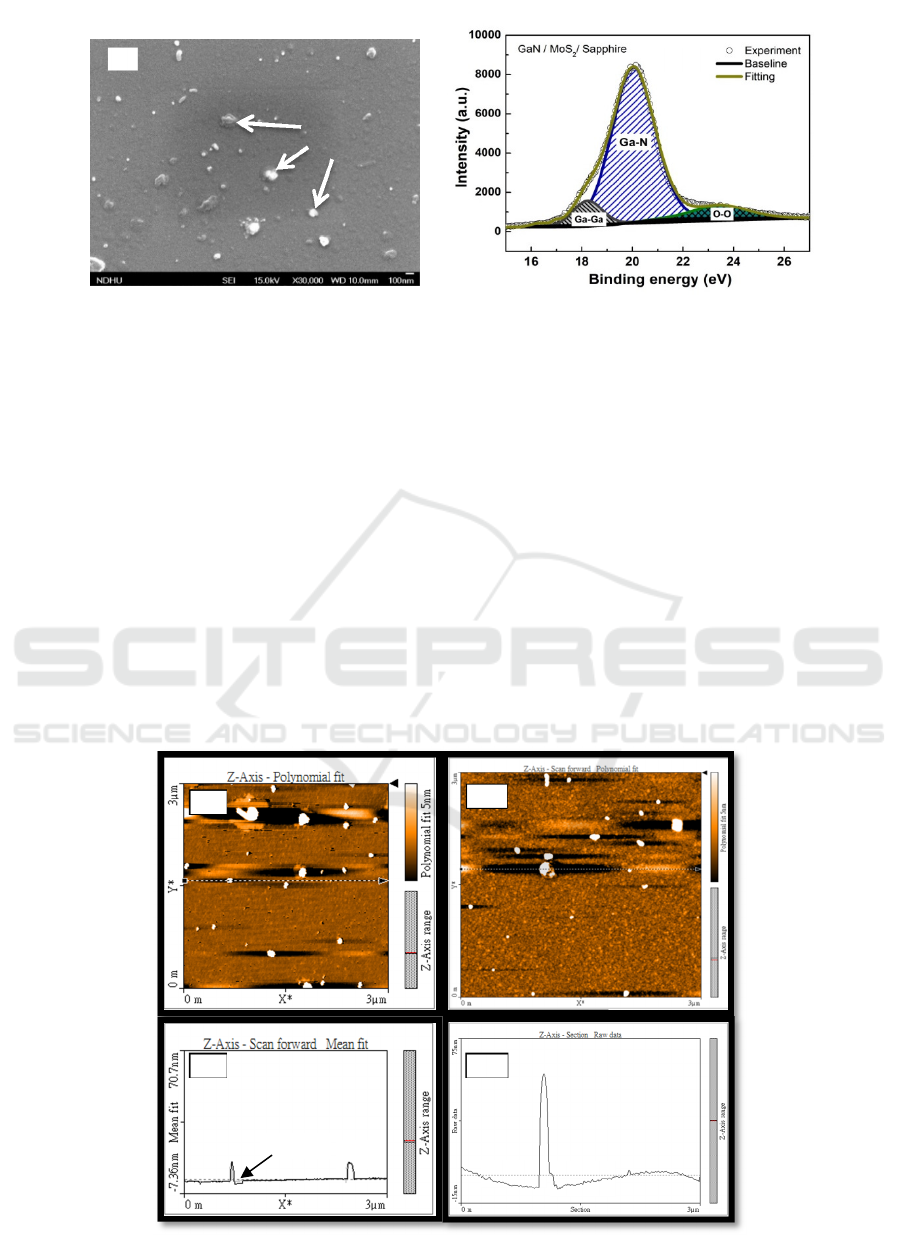
Morphology and surface composition of GaN films
served by SEM image and XPS fitting curve was
presented completely in Figure 1. The GaN films
grew and covered throughout on the surface of the
MoS
2
layer Figure 1(a). The morphology of GaN
films seems smooth with a large flat area indicating
that GaN was grown epitaxial by the 2D mode layer.
However, several Ga particles spread irregularly on
the surface with size in the range up to 150 nm.
Attending the particles associated with low growth
temperature on the system. The low heat energy
provided by the substrate might be caused the atoms
are not sufficiently mobile to reach the favourable
sites at the step edges (Susanto, Kan and Yu, 2017).
They are incorporated at random position and
accumulated to construct the cluster on the surface.
In Ga-rich growth condition, the particle can be even
bigger formed like the droplets on the surface. By
the less energy desorption, both Ga and N atoms
became retarded to mobilize in creating 2D layer
epitaxy. Further, the composition of Ga cluster
related to Ga metallic bonding will be inspected
carefully by the XPS measurement.
In Figure 1(b), the XPS result was demonstrated the
semi-quantitative analysis by the peak fitting of XPS
spectra. The surface composition of GaN film was
displayed in detail by de-convoluted Ga-3d core
level spectra. The peak positions of bonding
elements were located at 18.25, 20.05, and 23.50 eV
for Ga-Ga, Ga-N and O-O, respectively (Yu et al.,
2014; Mishra et al., 2015). Meanwhile, the
percentages of those bonding elements were 8.8,
81.0 and 10.2 %, serially. According to the results,
GaN bonding has been constructed on the surface of
the MoS2 layer with great composition related to a
higher percentage of 80 %. However, the presenting
of Ga-Ga bonding was formed due to the
accumulation of Ga atoms, deposited on the surface
of GaN films. The result was consistent with the
SEM result in Figure 1(a) that the Ga-Ga related
with Ga particles was come on the surface GaN
films(Susanto et al., 2017; Susanto, Kan and Yu,
2017). Unfortunately, there is an O-O bonding
element also detected in higher binding energy. It
could be related to oxygen absorbed on the GaN
surface as was contacted to the air. Furthermore, the
surface features correspond with morphology and
roughness condition will be observed clearly by
AFM.
Surface Texture of Thin Gallium Nitride Grown on Closed to Van Der Wall Layer of Molybdenum Disulfide
23
Ga particles
(a)
(b)
Figure 1. (a) SEM images and (b) De-convoluted Ga-3d XPS spectra for the surface composition of the GaN films
Detail of surface morphology of MoS
2
layers and
GaN films was exhibited clearly by AFM
observation in Figure 2 (a, c) and (b, d), serially. By
the scan area of 3 x 3 µm, the bright area likes
particles and the dark relates with thick striped
demonstrating the character both of surface feature.
The bright areas describe the pattern of rising
surface peaks, and dark areas illustrate the valleys
formed on the surface. The broader area of dark and
bright regions with a root mean square (RMS) of
3.01 nm was exhibited on the surface of MoS
2
in
Figure 2(a). After deposition of GaN films, the
reduction of those areas with RMS of 2.17 nm was
demonstrated on Figure 2(b). The reduction in the
size of these two regions represented that decline
peak and valley formed on the film’s surface. The
narrowing of both areas could describe that a
smoother surface has constructed on the GaN films.
Moreover, the line roughness will be confirmed
more clearly with one dimension of contour scan in
Figure 2(c), (d) demonstrating the profile of the
valley and peaks feature. They can be compared to
the results from the striped scan in Figure 2 (c) and
(d). There are several grooves with a smaller curve
in Figure 2(c) than in Figure 1(d). The curve relates
to the peak formed on the surface layer, while the
groove correlates with the valley constructed on the
surface as well. The high peak and the deep of the
valley for both surface contours is 0.51 nm and 0.31
nm for MoS
2
layer, and 1.11 nm and 0.73 nm for
GaN films, respectively. Based on the AFM results,
the surface of GaN film was smoother than the MoS
2
layer even though the peak and valley GaN films
higher and deeper than the MoS
2
layer. It could be
come due to the line roughness of the GaN film
taken in the highest and the deepest area.
Figure 2. (a) 2D AFM images of the surface of MoS
2
/Sapphire and (b) GaN films with scan area 3 x 3 µm, while (c) scan
profile contour as long 3 µm on MoS
2
/Sapphire and (d) for GaN films.
(b)
(c) (d)
(a)
Pea
k
Groove
Valley
Valley
Ga-3d
Pea
k
ASAIS 2019 - Annual Southeast Asian International Seminar
24

4 CONCLUSIONS
In conclusion, we are successful to deposit the GaN
films on the MoS
2
layer by the MBE system. The
surface texture of the GaN films formed was a
smooth surface with a large flat area correlated with
the 2D mode layer. The great of Ga-N bonding
created on the surface with less Ga-Ga and O-O was
obtained higher than 80 %. The reduction of surface
roughness was initiated by the GaN layer covered
the substrate. The RMS of GaN film with scan area
3 x 3 µm was archived at 2.17 nm. The diminution
of peak size and groove related to the valley was
also demonstrated on the contour of the scan profile.
However, attending several Ga particles spread
irregularly on the surface with size in the range up to
150 nm that was constructed due to low growth
temperature provided by the system. Further, the
higher growth temperature served by substrate could
facilitate the smoother surface of GaN film with the
minimum of Ga metallic.
ACKNOWLEDGMENTS
All authors would like to thank to Ministry of
Research and Technology / Research Council and
National Innovation Republic of Indonesia (BRIN)
and also Ministry of Science and Technology,
Taiwan for financially supporting this study (MOST
107-2221-E-259- 001-MY2 and 107-3017-F-009-
002).
REFERENCES
Aissat, A. and Vilcot, J. P. (2019) ‘Development of
InxGa1-xN/GaN axial multiple quantum well
nanowire for solar cell applications’, Optik. Elsevier
GmbH., p. 163844. doi: 10.1016/j.ijleo.2019.163844.
Ajayan, P., Kim, P. and Banerjee, K. (2016) ‘Two-
dimensional van der Waals materials’, Physics Today,
69(9), pp. 38–44. doi: 10.1063/PT.3.3297.
Chapin, C. A. et al. (2017) ‘InAlN/GaN high electron
mobility micro-pressure sensors for high-temperature
environments’, Sensors and Actuators, A: Physical.
Elsevier B.V., 263, pp. 216–223. doi:
10.1016/j.sna.2017.06.009.
Chen, Y. et al. (2017) ‘High efficiency GaN LEDs with
submicron-scale 2D periodic structures directly
fabricated by laser interference ablation’, Optics and
Laser Technology. Elsevier, 90(August 2016), pp.
211–215. doi: 10.1016/j.optlastec.2016.08.019.
Chen, Y. et al. (2019) ‘GaN in different dimensionalities:
Properties, synthesis, and applications’, Materials
Science and Engineering R: Reports, 138(January), pp.
60–84. doi: 10.1016/j.mser.2019.04.001.
Choi, W. et al. (2017) ‘Recent development of two-
dimensional transition metal dichalcogenides and their
applications’, Biochemical Pharmacology. The
Author(s), 20(3), pp. 116–130. doi:
10.1016/j.mattod.2016.10.002.
Ho, Y. T. et al. (2015) ‘Layered MoS
2
grown on c -
sapphire by pulsed laser deposition’, Physica Status
Solidi - Rapid Research Letters, 9(3), pp. 187–191.
doi: 10.1002/pssr.201409561.
Husna Hamza, K. and Nirmal, D. (2020) ‘A review of
GaN HEMT broadband power amplifiers’, AEU -
International Journal of Electronics and
Communications. Elsevier GmbH, p. 153040. doi:
10.1016/j.aeue.2019.153040.
Kuwano, N. et al. (2014) ‘Behavior of defects in a-plane
GaN films grown by low-angle-incidence
microchannel epitaxy (LAIMCE)’, Journal of Crystal
Growth. Elsevier, 401, pp. 409–413. doi:
10.1016/j.jcrysgro.2013.11.032.
Liu, L. and Edgar, J. H. (2002) ‘Substrates for gallium
nitride epitaxy’, Materials Science and Engineering:
R: Reports, 37(3), pp. 61–127. doi: 10.1016/S0927-
796X(02)00008-6.
Liu, Y. et al. (2019) ‘Transferable GaN Films on
Graphene/SiC by van der Waals Epitaxy for Flexible
Devices’, Physica Status Solidi (A) Applications and
Materials Science, 216(11), pp. 1–6. doi:
10.1002/pssa.201801027.
Mishra, M. et al. (2015) ‘Pit assisted oxygen
chemisorption on GaN surfaces’, Physical Chemistry
Chemical Physics. Royal Society of Chemistry,
17(23), pp. 15201–15208. doi: 10.1039/c5cp00540j.
Mynbaeva, M. G. et al. (2016) ‘TEM study of defect
structure of GaN epitaxial films grown on GaN/Al
2
O
3
substrates with buried column pattern’, Journal of
Crystal Growth. Elsevier, 445, pp. 30–36. doi:
10.1016/j.jcrysgro.2016.04.011.
Susanto, I. et al. (2017) ‘Effects of N/Ga flux ratio on GaN
films grown on 4H-SiC substrate with 4° miscutting
orientation by plasma-assisted molecular beam
epitaxy’, Journal of Alloys and Compounds. Elsevier
B.V, 710, pp. 800–808. doi:
10.1016/j.jallcom.2017.03.320.
Susanto, I. et al. (2019) ‘Morphology and surface stability
of GaN thin film grown on the short growth time by
Plasma Assisted Molecular Beam Epitaxy’, J. Phs :
Conference Seriese, 1364(012067). doi:
10.1088/1742-6596/1364/1/012067.
Susanto, I., Kan, K. and Yu, I. (2017) ‘Temperature
effects for GaN fi lms grown on 4H-SiC substrate with
4 miscutting orientation by plasma-assisted molecular
beam epitaxy’, Journal of Alloys and Compounds.
Elsevier B.V, 723, pp. 21–29. doi:
10.1016/j.jallcom.2017.06.224.
Susanto, I., Tsai, C.-Y., et al. (2019) ‘The influence of 2D
MoS
2
layers on the growth of GaN films by plasma-
assisted molecular beam epitaxy’, Applied Surface
Surface Texture of Thin Gallium Nitride Grown on Closed to Van Der Wall Layer of Molybdenum Disulfide
25

Science, 496(July), p. 143616. doi:
10.1016/j.apsusc.2019.143616.
Tian, J. et al. (2019) ‘Optoelectronic properties of two-
dimensional GaN adsorbed with H, N and O: A first-
principle study’, Physics Letters, Section A: General,
Atomic and Solid State Physics. Elsevier B.V.,
383(24), pp. 3018–3024. doi:
10.1016/j.physleta.2019.06.007.
Wan, Y. et al. (2018) ‘Epitaxial Single-Layer MoS
2
on
GaN with Enhanced Valley Helicity’, Advanced
Materials. doi: 10.1002/adma.201703888.
Yamada, a. et al. (1999) ‘Molecular beam epitaxy of GaN
on a substrate of MoS
2
layered compound’, Applied
Physics A: Materials Science & Processing, 69(1), pp.
89–92. doi: 10.1007/s003390050976.
Yang, Z. P. et al. (2017) ‘Effects of substrate and
annealing on GaN films grown by plasma-assisted
molecular beam epitaxy’, Surface and Coatings
Technology. Elsevier B.V., 320, pp. 548–553. doi:
10.1016/j.surfcoat.2016.11.019.
Yu, I.-S. et al. (2014) ‘Characterization and density
control of GaN nanodots on Si (111) by droplet
epitaxy using plasma-assisted molecular beam
epitaxy.’, Nanoscale research letters, 9(1), p. 682. doi:
10.1186/1556-276X-9-682.
Zhang, Z. et al. (2018) ‘Interface Engineering of
Monolayer MoS
2
/GaN Hybrid Heterostructure:
Modified Band Alignment for Photocatalytic Water
Splitting Application by Nitridation Treatment’, ACS
Applied Materials and Interfaces. doi:
10.1021/acsami.8b01286.
ASAIS 2019 - Annual Southeast Asian International Seminar
26
