
Design and Implementation Buc
k
-boost Converter using Arduino
Mega 2560
Andhika Giyantara, David Christover and Yun Tonce Kusuma Priyanto
Institut Teknologi Kalimantan
Keywords: Buck-boost, Converter, Duty cycle.
Abstract: Nowadays, the development of technology cannot be separated from energy demands. An increasing energy
requirement needed power electronic circuits to support systems that are producing a direct voltage or
commonly called Direct Current (DC). A problem obtained is to convert the desired voltage level according
to desired requirements. The development of power electronic circuits can be solving these problems by using
a DC-DC converter topology. In general, DC-DC converters have several topologies such as buck converter,
boost converter, buck-boost converter, and Cuk converter. In this research, an inverting buck-boost converter
topology is designed and implemented to increasing and decreasing voltage. The aim of this research is
converting the input DC voltage value to the constant output DC voltage value. A value of duty cycle
configuration is depending switch on and switch off from MOSFET, which generated from Arduino Mega
2560. The results of the average output voltage value from the mathematical condition is 12 Volt; after that,
from simulation condition is 12,05 Volt and then from implementation condition is 9,92 Volt. The results of
the average ripple output voltage from the mathematical condition are 0,4%, after that from the simulation is
0,79% and then from implementation condition is 0,56%. The results of the average ripple value current from
the mathematical condition are 6.54% and then from simulation condition is 6.94%. Finally, the buck-boost
converter system that has been designed from this research has obtained an average value of power efficiency
in the simulation conditions is 65.12% and then from implementation condition is 74,87%.
1 INTRODUCTION
The development of power electronics has played a
role in everyday life to produce a Direct Current
(DC). DC voltage is generated by the process of
converting DC input voltage to DC voltage for lower
or higher output desired. This DC voltage conversion
is commonly referred to as DC-DC Converter. The
application of DC-DC converters on an electronic
device has made it possible to use resources that have
relatively small voltage values such as batteries and
batteries, where the output voltage source can be
adjusted according to usage requirements (Forouzesh,
2017).
DC-DC converter or known as DC chopper, is
often used as a DC voltage regulator, both decreasing
and increasing voltage. In general, DC voltage
generated from renewable energy sources is volatile
because it is caused by natural factors such as light
intensity. Currently, the application of the DC-DC
converter is widely applied to renewable energy
sources such as solar panels (Choudhary, 2014). DC
Chopper consists of several configurations, and the
most commonly used is DC Chopper types of Buck,
Boost, Buck-Boost, Cuk, and SEPIC. The buck
converter system is a non-isolated switching type DC
converter that can reduce the output voltage and then
boost converter, which can increase the voltage by
adjusting the duty cycle from Pulse Width
Modulation (PWM) (Rashid, 2014).
The disadvantages of the buck converter and
boost converter can only step down or step up the
output voltage level that given and cannot be used in
both conditions. When we set a variable input voltage
value to be constant, a combination of the buck-boost
converter can be used (Kazimierczuk, 2008).
Recently, Arduino microcontrollers are becoming
increasingly popular in various studies (Jinook,
2016). This open-source platform has been developed
for prototype purposes and is based on easy-to-use
hardware and software, providing researchers with
key features that can translate into both economic and
practical benefits (Buesa, 2019). When we applied the
buck-boost converter with an integrated energy
Giyantara, A., Christover, D. and Priyanto, Y.
Design and Implementation Buck-boost Converter using Arduino Mega 2560.
DOI: 10.5220/0009443301690176
In Proceedings of the 1st International Conference on Industrial Technology (ICONIT 2019), pages 169-176
ISBN: 978-989-758-434-3
Copyright
c
2020 by SCITEPRESS – Science and Technology Publications, Lda. All rights reserved
169

source, it is better to use a microcontroller that has
many digital or analog pins such as Arduino
microcontrollers and also can be used to generate
PWM for switching components. Therefore, in this
research, we applied the design and implementation
of the buck-boost converter using ArduinoMega 2560
as an alternative solution to maintaining a constant
output voltage with varying input voltage and can be
applied to renewable energy sources.
2 RELATED WORK
Padillah, Syahrial and Saodah (2014) applied the
switching type DC voltage converter topology, which
could increase the boost output voltage. The
converter output voltage was controlled by the
magnitude adjusting of the signal duty cycle of pulse
width modulation (PWM), that generated by using the
microcontroller of phase correct PWM mode. The
results of the converter output voltage were designed
for 48 Volt. The test used the variable resistance load
by measuring the voltage and current at both the input
and output sides. The test performance was used to
determine the efficiency of the boost converter to
change in the load and duty cycle.
Muthukrishnan (2014) also studied about boost
converter. In this research, about boost converter
specialty is achieved 10 times that of input voltage,
and more than 10 times of input voltages is possible
from the output side by using coupled inductor and
parallel capacitor. The output voltage is high, and the
voltage stress across the active switch is minimized,
and output ripples also minimized. (Chin Wei Chang
et al., 2011) applied to prolong the service time of
batteries, a good power management strategy should
have high conversion efficiency and also take
advantage of the full battery voltage range. There are
three types of regulators- linear regulations, switching
regulators, and switched-capacitor-based converters.
The switching regulator is chosen in this research
because it can achieve the highest efficiency among
them
Khalif Ahadi (2012) explaining about design buck
converter. Two units of a buck converter using P-
Channel MOSFET (Metal Oxide Semiconductor
Field Effect Transistor) and N-type IGBT (Insulated
Gate Bipolar Transistor) as a switch are already
designed. Experimental results show each buck
converters are able to flow a current as high as 60
Ampere on the adjusted voltage of 12.6 volts, but this
output voltage is still fluctuating influenced by the
input voltage and load. The efficiencies also fluctuate,
but they'll reach above 60% under maximum load.
(Arif Muslih Jainudin et al., 2017) also studied DC-
DC converter, which concentrated in a buck
converter. The switching component used in this
research is the MOSFET IRFZ44N type. Based on the
measurement results, buck converter with feedback
can constrain the output current on 1 Ampere.
Meanwhile, when the output voltage feedback
working, the value of output voltage can be
constrained on 14,4 Volt, and 13,5 Volt with the
average efficiency of buck converter without
feedback was 87,39%.
Viswanatha (2017) studied circuit modeling,
design, simulation, and analysis of non-inverting
buck-boost converter. In this research, a voltage
control technique is employed to regulate the output
voltage irrespective of the variations in input voltage
and load variations. To generate the PWM signals to
turn on and off the switches of the converter, the
control circuit is employed, which consists of very
simple basic logic gates to realize closed-loop control
with good regulations of load and line. This method
can be replaced by the current control technique to
generate the pwm signals to regulate the output
voltage. A non-inverting converter can be used in the
photovoltaic system, which uses a conventional buck-
boost converter to charge the battery. Noninverting
converters will replace the conventional buck-boost
converters used in the battery charging alongside the
MPPT logic. (Farah Shabila Dinniyah, 2017) also
applied DC-DC converter. This research discusses
designing a buck-boost converter for solar panels,
with a voltage input range of 10 to 50 Volt. The
regulation of output voltage is the main aim in
analyzing the success of the design created. The
design is simulated with Proteus 8.4 and yields a
voltage output with an efficiency of ninety to ninety-
nine
In summary, the previous studies used different
features and methods for step down and step up
output voltage desired; after that, these studies were
limited in simulation only, especially a buck-boost
converter. So in this research, we design and
implementation of buck-boost converter using
Arduino Mega2560 and which consists of the
specification with a voltage ripple and current ripple
desired.
ICONIT 2019 - International Conference on Industrial Technology
170
3 IMPLEMENTATION OF BUCK-
BOOST CONVERTER
3.1 System Architecture
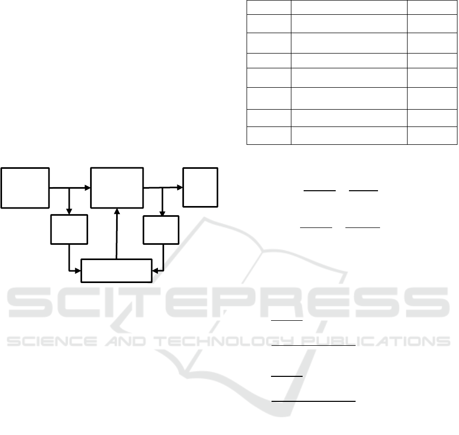
The proposed DC converter system, as shown in
Fig.1, consists of five main components: 1, DC power
variable; 2. buck-boost converter; 3, a resistive load;
4, a microcontroller and 5, measuring tools such as
AVO meter and oscilloscope. The key from the buck-
boost system is regulating a voltage output value to
be a constant value, which considers the variation of
input voltage from the DC power variable and the
value of the duty cycle.
Figure 1: Proposed of block diagram system
The buck-boost converter system process started
from input voltage variation, which obtained with a
DC variable source. The value of the voltage and
current variable readings that have been obtained
from measuring tools is used as a reference to do the
large duty cycle used. The microcontroller used in
this research is ArduinoMega 2560. A value of the
duty cycle that has been programmed is processed in
the microcontroller to generate PWM for the duty
cycle desired. The results of the PWM then forwarded
for the gate at the MOSFET to be able to set the
switching on the MOSFET. The value of the output
voltage depends on the amount of duty cycle given to
the system. If the duty cycle value is below 50%
system will be in a buck condition, and vice versa, if
the value of the duty cycle is above 50% system, it
will be in a boost condition.
3.2 Calculation of Components
In this research, we designed the specification of the
buck-boost system as a reference for calculating
component values.
Table 1: List of Parameters.
Legend Specification Value
Minimum voltage input 7 V
Maximum voltage input 17 V
Voltage output 12 V
∆
Voltage ripple <1%
∆
Current ripple <10%
Frequency switching 62500 Hz
Resistance 100 Ohm
3.2.1 Duty Cycle Value
12
712
63%
(1)
12
17 12
41% (2)
Based on specification from table 1, the results of
the duty cycle maximum from the equation above is
63%, and the duty cycle minimum is 41%.
3.2.2 Inductor Value
∆
7 0,63
62500 0,33 0,1
2171,75
(3)
∆
17 0,41
62500 0,20 0,1
5498,22
(4)
Mentioned to table 1, a limit of the current ripple
less than 10%. So, from equation 2 we got inductance
value on inductor is 5498,22 . Thus according to
the literature obtained, in this research, the inductance
on inductor value is 6 determined as a parameter
in the buck-boost converter system. The result of the
value on inductor that has been calculated in equation
2 used as a reference to determine the number of turns
needed to reach the inductance value on the inductor.
The calculation to find a number of turns an inductor
can be searched by equation 4. The result of
calculation using equation 4 obtained a number of
turns on the inductor is 27 turns by using a toroidal
design.
DC
Power
Variable
Buck-
Boost
Converter
Load
AVO
meter
Microcontroller
AVO
mete
r
Design and Implementation Buck-boost Converter using Arduino Mega 2560
171
6
22
7
62,14
6731 4
22
7
10
60
27
(5)
3.2.3 Capacitor Value
Then, by using a limit of the voltage ripple less than
1%, the result of calculation from equation 3 we
obtained the highest results from the minimum and
maximum duty cycle is 10,11 . From this result,
we can approach 20 .
∆
0,63
100 0,01 62500
10,1
(6)
∆
0,41
100 0,01 62500
6,62
(7)
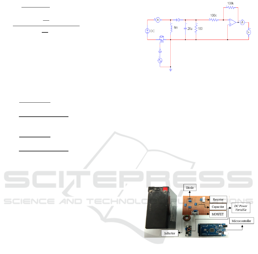
3.3 Design of Circuit Simulation
Figure 2 can be explained that an inverting buck-
boost converter circuit arranged into several
components, including voltage source DC, square
wave voltage source, on-off switch controller,
MOSFET switch, inductor, diode, capacitor, resistor,
inverting op-amp voltage probe, and a current probe.
In the simulation design, the condition of all the
components buck-boost converter is in the ideal
condition. The function of a square wave voltage
source is to initialize the parameters according to the
frequency value and the large duty cycle used. The
inverting component of the op-amp to obtain the
output voltage value measured in polarity according
to the input voltage source.
Figure 2: PSIM simulation circuit on the buck-boost
converter system.
3.4 Hardware Implementation
Figure 3 represents the results of the hardware that
was made in this research. Hardware that has been
implemented in accordance with Figure 2. In this
research, we using microcontroller ArduinoMega
2560 as a PWM control and then an active switching
component that is N-MOSFET IRFZ44N and passive
switching components that is diode Schottky
SR3100. A data obtained then processed to obtain the
ripple value generated at each specified test interval.
The results of this test after that processed to carry out
the overall analysis and make comparisons on each
condition.
Figure 3: Hardware implementation of the circuit on the
buck-boost converter system.
4 EXPERIMENTAL RESULTS
AND DISCUSSION
4.1 Analysis of Ripple Voltage in
Mathematical Condition
Based on the information from table 2, a value of
input voltage from 7 Volt gets the lowest accuracy
that is 49.6% with a ripple voltage of 0.060 Volt.
When an input voltage from 17 Volt gets the highest
accuracy value is 67.2% with a ripple voltage value
of 0.039 V. The value of deviation is a reduction in
the boundary of ripple voltage specification with
ICONIT 2019 - International Conference on Industrial Technology
172

voltage ripple value generated when the test is carried
out.
Table 2: Results of voltage ripple in mathematical
condition.
Voltage
ripple
(V)
Voltage
ripple
(%)
Deviation
(%)
Accuracy
(%)
7 0,060 0,504 0,496 49,60
8 0,058 0,480 0,520 52,00
9 0,055 0,456 0,544 54,40
10 0,053 0,44 0,560 56,00
11 0,049 0,416 0,584 58,40
12 0,048 0,400 0,600 60,00
13 0,046 0,384 0,616 61,60
14 0,044 0,368 0,632 63,20
15 0,042 0,352 0,648 64,80
16 0,041 0,344 0,656 65,60
17 0,039 0,328 0,672 67,20
4.2 Analysis of Current-Voltage in
Mathematical Condition
It can be seen from Table 3, the highest accuracy
value is when the system gave the lowest input
voltage value, or we can call it to boost condition. The
situation is inversely proportional when the system is
given the lowest voltage value or buck condition. The
difference value is a reduction of the current ripple
specification limit specified by the current ripple
value generated when the test is carried out. In table
information 3, a current ripple value of 9.08% is
generated when the system is given a maximum input
voltage value of 17 volts and inversely proportional
when given a minimum voltage value of 7 volts.
Table 3: Results of current ripple in mathematical
condition.
Current
ripple
(V)
Current
ripple
(%)
Deviation
(%)
Accuracy
(%)
7
0,012
3,61 6,39 63,89
8 0,013 4,27 5,73 57,33
9 0,014 4,89 5,11 51,14
10 0,015 5,56 4,44 44,44
11 0,015 6,08 3,92 39,21
12 0,016 6,67 3,33 33,33
13 0,017 7,21 2,79 27,89
14 0,017 7,71 2,29 22,94
15 0,018 8,15 1,85 18,52
16 0,018 8,74 1,26 12,63
17 0,019 9,08 0,92 9,20
4.3 Analysis of Ripple Voltage in
Simulation Condition
Based on the information from table 4, the largest
ripple value obtained when the system is given an
input voltage of 8 volts with a large duty cycle of
60%. The situation is inversely proportional when the
system is given an input voltage 12 volts with a 50%
duty cycle, which experiences the smallest voltage
ripple value. Analysis of the current ripple generated
in table 4 does not have results that exceed the
specified ripple limit of 1%. The results of the ripple
voltage analysis of the input voltage are in accordance
with the design specified in the information table 1.
Table 4: Results of voltage ripple in simulation condition.
Voltage
ripple
(V)
Voltage
ripple
(%)
Deviation
(%)
Accuracy
(%)
7 0,110 0,93
0,07 7
8 0,120 0,98 0,02 2
9 0,100 0,83 0,17 17
10 0,100 0,81 0,19 19
11 0,100 0,84 0,16 16
12 0,060 0,50 0,50 50
13 0,090 0,75 0,25 25
14 0,090 0,75 0,25 25
15 0,080 0,67 0,33 33
16 0,090 0,74 0,26 26
17 0,110 0,93 0,07 7
4.4 Analysis of Current-Voltage in
Simulation Condition
The results obtained from the information in table 5,
the highest accuracy value is at the lowest input
voltage level 7 Volt with the highest duty cycle of
63%. The situation is inversely proportional when the
system is configured to the highest voltage 17 Volt
with the lowest duty cycle, 41%. Analysis of the
current ripple value generated in the simulation does
not exceed the specifications specified in table 1. The
overall current ripple value produced in each input
voltage test is below 10% so that it matches the
system that has been designed.
Table 5: Results of current ripple in simulation condition.
Current
ripple
(V)
Current
ripple
(%)
Deviation
(%)
Accuracy
(%)
7
0,012
3,13 6,87 68,70
8 0,013 3,23 6,77 67,70
9 0,014 7,14 2,86 28,60
10 0,015 3,70 6,30 63,00
Design and Implementation Buck-boost Converter using Arduino Mega 2560
173
11 0,015 4,00 6,00 60,00
12 0,016 8,33 1,67 16,70
13 0,017 8,69 1,31 13,10
14 0,017 9,09 0,91 9,10
15 0,018 9,52 0,48 4,80
16 0,018 9,52 0,48 4,80
17 0,019 10,00 0 0
4.5 Analysis of Ripple Voltage in
Hardware Condition
In this case, we analyze the voltage ripple based on
information in table 6 using an oscilloscope and
obtained a maximum voltage level 7.02 Volt with a
duty cycle value of 63%, which exceeded the
specified ripple limit of 1%. The condition exceeds
the specified ripple voltage limit because when the
test is obtained, the switching component is in the hot
condition so that a fluctuating voltage value changes
on the installed capacitor. The accuracy value
obtained in the ripple voltage analysis on hardware is
dominated when the system is in a state of the buck
with a value above 60%, whereas when the boost
state, the accuracy value is below 40%.
Table 6: Results of voltage ripple in hardware condition.
Voltage
ripple
(V)
Voltage
ripple
(%)
Deviation
(%)
Accuracy
(%)
7,02
0,12
1,31
0,31 31,00
8,02 0,08 0,82 0,18 18,37
9,02 0,06 0,61 0,39 38,90
10,02 0,06 0,59 0,41 40,59
11,02 0,06 0,61 0,39 39,02
12,02 0,04 0,40 0,59 59,76
13,02 0,04 0,39 0,60 60,39
14,02 0,04 0,40 0,60 60,00
15,02 0,04 0,40 0,60 60,00
16,02 0,04 0,39 0,60 60,39
17,02 0,04 0,40 0,60 60,00
4.6 Comparison of Voltage Output
From the graph in figure 4, the value of output voltage
generated when the simulation condition gets a value
corresponding to output voltage value mathematical
condition. The results of output voltage when the
implementation produces the lowest value affected by
the condition of component is not ideal when tested.
The highest output voltage value when the
implementation condition is 10.23 Volt with a given
input voltage 16 Volt and a large duty cycle of 43%.
When the simulation condition, the highest voltage
value 12.33 Volt be produced with input voltage 10
Volt, and the duty cycle is 55%.
Figure 4: Results of output voltage
The biggest error value is when the
implementation condition maximum voltage level 7
Volt with the resulting error value of 22.33%. The
difference is obtained with the largest error value of
2.68 Volt against the value of voltage specified at 12
Volt. The results of output voltage values in the
implementation conditions do not match the setpoint
voltage specified that has been designed, but the
system successfully increases and decreases from the
input voltage.
4.7 Comparison of Voltage Ripple
In Figure 5, we can infer from mathematical,
simulation, and implementation conditions. The
lowest voltage ripple value is when the system gave
input voltage 12 Volt and a large duty cycle of 50%.
Figure 5: Results of voltage ripple
From the implementation condition, it can be
inferred that the smaller value in input voltage given,
the greater the ripple value of the resulting voltage.
Likewise, if the input voltage value is very large, the
ripple of value resulting voltage is getting smaller.
This is because the error value is obtained so that the
0
2
4
6
8
10
12
14
7 8 9 1011121314151617
Output Voltage (V)
Input Voltage (V)
Mathematical
Condition
Simulation
Condition
Implementation
Condition
0
0.2
0.4
0.6
0.8
1
1.2
1.4
7 8 9 10 11 12 13 14 15 16 17
Ripple Voltage (%)
Input Voltage (V)
Mathematical
Condition
Simulation
Condition
Implementation
Condition
ICONIT 2019 - International Conference on Industrial Technology
174

value of the output voltage is very fluctuating, which
can make an increase in voltage ripple generated. If
the error value obtained is greater, the accuracy value
decreases and, as a result, is the increase of the ripple
generated from the circuit.
4.8 Comparison of Ripple Current
The result of the graph in figure 6, the current ripple
value increases when the value of the input voltage
given increases. The smallest ripple value is 3.61%
when the mathematical condition, and then from
simulation condition, is 3.13%. The results of the
current ripple value generated in each condition in
accordance with the current ripple value limit that has
been designed in the information from table 1. The
maximum current ripple value is 10% from the
mathematical condition when the system is given a
maximum voltage value 17 Volt with duty cycle 41%.
However, the maximum ripple current is still in
accordance with the specified ripple current limit of
10%.
Figure 6: Results of ripple current
4.9 Comparison of Efficiency
In this session, we analyze efficiency by comparing
the simulation with the hardware that has been
implemented. The incoming power from each input
voltage will be calculated with the output power
generated.
Figure 7: Results of power efficiency
In figure 7, the greatest efficiency value is
obtained from the implementation condition. From
our research, it is obtained that the power value on the
input side increases when the value of the input
voltage given increases. The average value of input
power is 2.24 Watt under simulation condition and
1.3 Watt during implementation condition. Power
values on the output side when simulation and
implementation conditions tend to be stable with an
average value of 1.45 Watt during simulation
conditions and 0.97 Watt during implementation
conditions. In the implementation condition, the
largest efficiency value of 84.44% is obtained with a
maximum input voltage level of 17 Volt with a
minimum duty cycle of 41%.
5 CONCLUSION AND FUTURE
WORK
This research used a buck-boost as a DC-DC
regulator and then can produce output voltage greater
or less than the input voltage. The polarity of the
buck-boost output voltage is inversely proportional to
the input voltage (voltage inverting).
This study also success in applying specification
limits to the determination of ripple current and
voltage buck-boost converter. In mathematical and
simulation conditions, the output voltage value
approaches the specified setpoint 12 Volt, but in the
simulation conditions, it is only able to produce an
average voltage value 9,92 Volt. The current ripple
results generated in mathematical and simulation
conditions are still in accordance with specifications
of less than 10%. The results of voltage ripple in
mathematical and simulation conditions are also
according to specifications of less than 1%, but when
0
2
4
6
8
10
12
7 8 9 1011121314151617
Ripple Current (%)
Input Voltage (V)
Mathematical
Condition
Simulation
Condition
0
10
20
30
40
50
60
70
80
90
7 8 9 1011121314151617
Efficiency (%)
Input Voltage (V)
Simulation
Condition
Implementation
Condition
Design and Implementation Buck-boost Converter using Arduino Mega 2560
175

the implementation condition for input voltage value
7 Volt increases above a predetermined limit.
Based on the results obtained in this study, some
recommendations were obtained, namely the addition
of a controller to the response of the output voltage
generated and the use of bootstrap capacitors in the
switching components used.
REFERENCES
Moore, R., Lopes, J., 1999. Paper templates. In
TEMPLATE’06, 1st International Conference on
Template Production. SCITEPRESS.
Smith, J., 1998. The book, The publishing company.
London, 2nd edition.
Ahadi, Khalif., 2012. “Rancang bangun buck converter 12
volt 60 ampere menggunakan P-Channel MOSFET dan
IGBT tipe N”. Jurnal Ketenagalistrikan dan Energi
Terbarukan. Pusat Penelitian dan Pengembangan
Teknologi Ketenagalistrikan, Energi Baru Terbarukan
dan Konservasi Energi.
Biel, Domingo. Enric Fossas. Josep M. Olm. 2007. “Robust
step-up DC/AC conversion with a full-bridge non-
inverting buck-boost”. IEEE International Conference
on Control Applications.
Buesa, Jaime Gonzales. Maria L. Salvador. 2019. “An
Arduino-based low cost device for the measurement of
the respiration rates of fruits and vegetables”. Elsevier.
Instituto Agroalimentario de Aragon. Spain
Chang, Chin Wei. Chia Ling Wei. 2011. “Single-inductor
four-switch non-inverting buck-boost DC-DC
converter”. IEEE.
Choudhary, Dhananjay. Ammol Ratna Saxena., 2014. “DC-
DC buck converter for MPPT of PV system”.
International Journal of Emerging Technology and
Advanced Engineering (IJETAE).
Daniel, W. Hart. 1997 “Introduction to Power Electronics
Handbook”. Valparaiso University. Indiana
Dinniyah, Farah Shabilah. Wahidin Wahab. Muhammad
Alif 2017. “Simulation of buck-boost converter for
solar panels using PID controller”. International
Conference AREQ.
Forouzesh, Mojtaba. Yam P. Siwakoti. Saman A. Gorji.
2017. “Step-Up DC–DC Converters: A Comprehensive
Review of Voltage-Boosting Techniques, Topologies,
and Applications”. IEEE Transactions on Power
Electronics.
Jainudin, Arif Muslih. Agung Warsito. Trias Andromeda.
2017. “Konverter arus searah tipe buck dengan umpan
balik arus dan tegangan untuk pengisi akumulator”.
TRANSIENT.
Jinook, oh. 2016. “An open source automatic feeder for
animal experiments”. Elsevier. Cognitive Biology
Department, University of Vienna, Althanstrasse.
Austria
Jin, G. W.T Ng. 2014. “An integrated tri-mode non-
inverting buck-boost DC-DC converter with segmented
power devices and power transmission gate structure”.
IEEE International Symposium on Power
Semiconductor Devices.
Kazimierczuk, Marian. 2016. “Pulse width modulated DC-
DC power converters”. John Wiley&Sons, Ltd.
America.
Khadiri, Karim El. Hassan Qjidaa. 2014. “Inverting buck-
boost DC-DC converter design challenges”.
International Journal of Embedded Systems and
Applications (IJESA).
Muthukrishnan. Dhanasekaran. 2014. “DC- DC boost
converter for solar power application”. Journal of
Theoretical and Applied Information Technology.
Padillah, Fitra. Syahrial. Siti Saodah. 2014. “Perancangan
dan realisasi konverter DC-DC tipe boost berbasis
mikrokontroler ATMega 8535”. Reka Elkomika
Journal.
Rashid, Muhammad H. “Power Electronics Circuits,
Devices, and Applications Handbooks”. Teknik
Elektro. Universitas Purdue. 2014.
S, Savitha. Vibin C Thomas. 2014. “PSIM Simulation of a
buck-boost DC-DC Converter with wide conversion
range”. International Journal of Engineering Research
and Technology (IJERT)
V, Viswanatha. Venkata Siva Reddy. 2017.
“Modeling,simulation and analisis of non-inverting
buck-boost converter using PSIM”. International
Conference on Circuits, Controls, Communications,
and Computing (I4C).
Zhang, Neng. Sam Batternally. Kai Chin Lim. 2017.
“Analysis of the non-inverting buck-boost converter
with four-mode control method”. IEEE.
ICONIT 2019 - International Conference on Industrial Technology
176
