
A New Design Method for Emitter Finger Space of Heterojunction
Bipolar Transistors
Chuantao Ma
1, a
1
College of Physics and Electronic Engineering, TaiShan University, TaiAn, China
a
mcht1016@163com
Keywords: Heterojunction bipolar transistors, silicon–germanium, segmented emitter, thermal stability.
Abstract: A new design method for emitter finger space of multi-finger HBT was proposed to improve thermal
stability of HBT. The 3-D temperature distribution, cross section temperature distribution, cross section
temperature gradient distribution of five-finger power HBT with traditional emitter structure and non-
uniform emitter finger space structure at the same dissipation power are given. Compared with 3-D
temperature distribution and cross section temperature distribution, the difference between traditional
emitter structure and non-uniform emitter finger space structure is more distinctive, so the cross-section
temperature gradient distribution is more effective for the design technique of non-uniform finger spacing of
multiple finger power HBT.
1 INTRODUCTION
Heterojunction bipolar transistors (HBT) has
become increasingly popular in power amplifiers for
wireless communications and microwave
applications because of its high-speed performance,
low-noise, high cutoff frequency and compatibility
with BiCMOS technology (S. P. McAlister, et.al,
2004; Wang Y, et.al, 2007; A Schuppen, et.al, 1995;
C Kermarrec, et.al, 1994). HBT usually employ a
multi-finger structure to improve the current
handling capability and thermal dissipation
capability. However, self-heating effects caused by
the temperature rise due to the power dissipation and
thermal coupling effects among emitter fingers
result in a higher temperature at the center fingers.
Because of the positive temperature coefficient of
emitter current, the center fingers conduct more
current and consequently generate more heat, which
eventually makes the device to become unstable at
high power and seriously limit the power handling
capability of the device.
In order to get high thermal stability under high
power dissipation, one method of non-uniform
finger spacing is usually proposed. Analytical and
experiment are used to investigate thermal behavior
of multiple finger heterojunction bipolar transistors
(HBT’s) with the non-uniform mitter-finger spacing.
For the non-uniform finger spacing HBT, the heat
flow from adjacent to the center finger is reduced by
increasing the spacing between fingers. It is shown
that the HBT with non-uniform finger spacing have
lower peak temperature in the device center, smaller
temperature difference between fingers compared
with HBT with uniform finger spacing under the
same power dissipation. These results indicate that
the method of non-uniform finger spacing is very
useful for getting the HBT with high thermal
stability. But it is difficult to get Suitable emitter
finger space of multi-finger HBT using a
comprehensive model for the multi-finger HBT
including the effects of temperature dependence of
thermal conductivity, and non-uniform, two-
dimensional temperature distribution on the emitter
fingers.
In this paper, a 3-D thermal simulation is
performed by the finite element method (FEM) in
ANSYS (A Schuppen, et.al, 1996; P A Potyraj, et.al,
1996; W. Liu, B. Bayraktaroglu, 1993; Willian Liu,
Ali Khatibzadeh, and Jim Sweder, 1996; J. -S. Rieh,
et.al, 2002; Jae-Sung Rieh, et.al, 2005). The results
of simulation show that temperature gradient can be
used to support a new method for the design of
emitter finger space of HBT.
398
Ma, C.
A New Design Method for Emitter Finger Space of Heterojunction Bipolar Transistors.
DOI: 10.5220/0008865203980401
In Proceedings of 5th International Conference on Vehicle, Mechanical and Electrical Engineering (ICVMEE 2019), pages 398-401
ISBN: 978-989-758-412-1
Copyright
c
2020 by SCITEPRESS – Science and Technology Publications, Lda. All rights reserved
2 THEORY
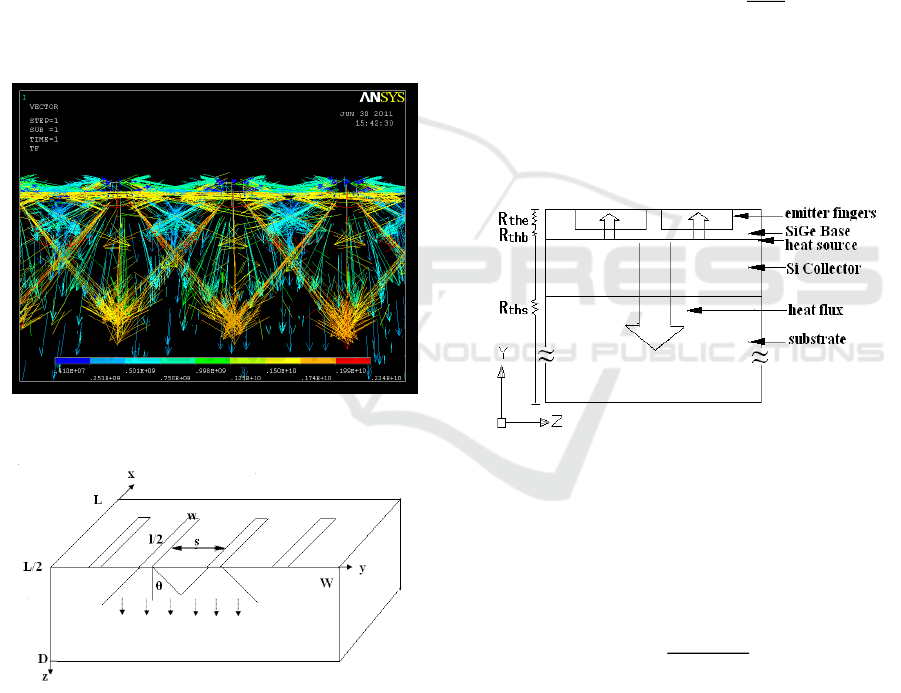
Figure.1 shows the bulk heat flux distribution of
multi-emitter HBT through the ANSYS finite
analysis software. When the HBT is working, the
temperature will gradually rise. The heat will send
out from the chip to the outside. When the
temperature don’t rise, the transistor achive a
thermal stable state. According to the theory of heat
conduction, the heat flux will move from the area of
the high temperature to the area of the low
temperature. Therefore, two adjacent emitter fingers
with the same power have the same heat flux
condition. The temperature of intermediate point is
the highest. The heat flux downward
conduction after meeting. The heat flux no longer
disperse to the two sides. we establish the thermal
resistance model as shown in Figure.2.
Figure 1. Bulk heat flux distribution of multi-emitter HBT.
Figure 2. The thermal resistance model of a multi-finger
HBT.
The device discussed in this study mainly
consists of two parts: active region and substrate as
shown in Fig. 3 (P A Potyraj, et.al, 1996; W. Liu, B.
Bayraktaroglu, 1993; Willian Liu, et.al, 1996). Heat
dissipation originates from the base-collector
junction, and through two opposite directions:
upward through emitter fingers and downward
through substrate. For the downward case, since the
thickness of collector layer is small enough
compared with the substrate, the thermal resistance
of substrate (Rths) was only considered. The upward
dissipation can be accounted as two pieces of
thermal resistor (Rthe and Rthb) representing the
thermal resistance from emitter and base,
respectively. The thermal resistance of the device
can be expressed as a series combination of partial
thermal resistances from very thin slabs along the
heat flux:
,
i
th th i
ii
ii
t
RR
kA
(1)
Where Rth is the thermal resistance, k is the
thermal conductivity of the medium, A is the
effective area of the heat conduction, t is the
thickness of the thin slab, and i is the number of the
slabs.
Figure 3. Cross-section of SiGe HBT showing heat flux,
heat source, and thermal resistance components.
The thermal resistance for the device can be
calculated from maximum temperature and
dissipation power:
max 0
th
diss
TT
R
P
(2)
Where Tmax is the maximum temperature of the
device, T0 is ambient temperature.
3 RESULTS AND DISCUSSION
In order to make sure the precision of the simulation,
there are two important steps in the thermal
A New Design Method for Emitter Finger Space of Heterojunction Bipolar Transistors
399
simulation: substrate simulation and active region
simulation. The stepped simulation avoids the
negative effect of the huge disparities of dimension
among each part (the thickness of emitter is 200nm
whereas it is up to 150mm for the substrate), ensures
the view of the 3-D thermal distribution in active
region clearly. For the first step, the model contains
heat source, collector layer, and substrate. We apply
the boundary temperature to the bottom of substrate
and dissipation power to the B-C junction. It was
assumed that the operating temperature of substrate
is ambient temperature at 300K. In second step, the
model of the active region consists of three parts:
emitters, base and collector. The dissipation power is
determined by collector current (Ic) and supply
voltage (Vce). In SiGe HBT device, collector current
must be less than Icritical which is the critical
collector current before current gain collapse occurs.
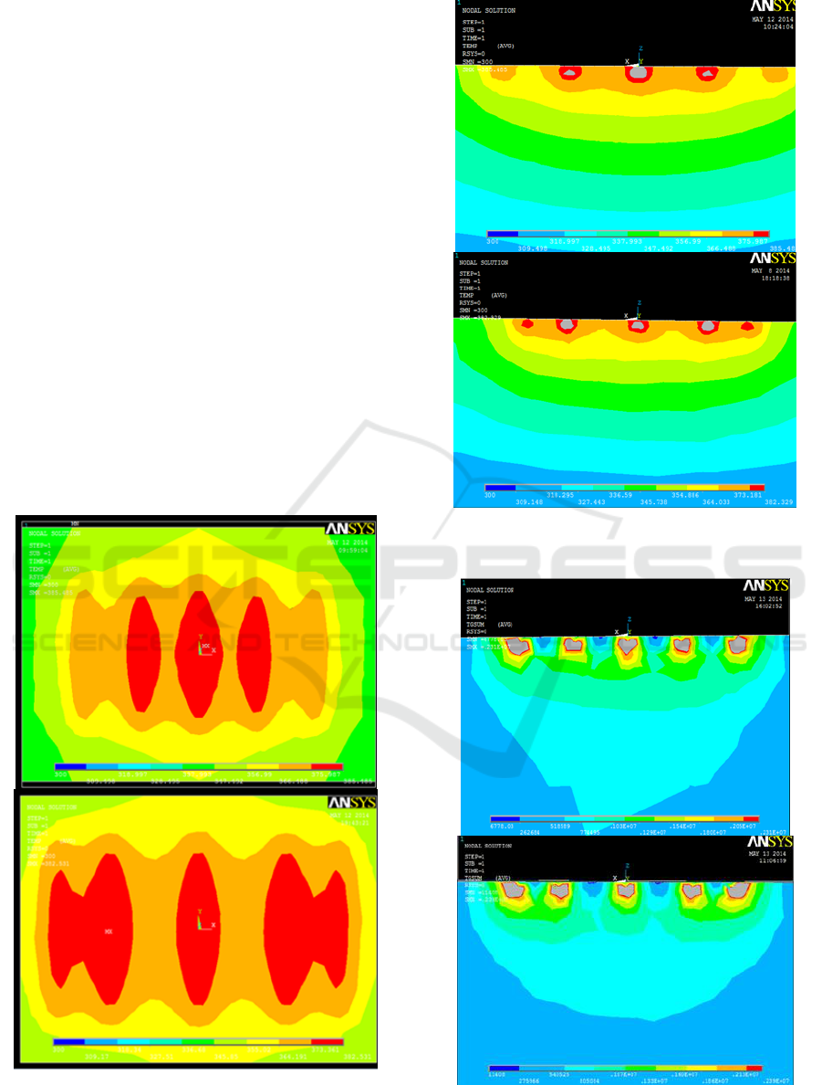
The 3-D temperature distribution, cross section
temperature distribution, cross section temperature
gradient distribution of five-finger power HBT with
traditional emitter structure and non-uniform emitter
finger space structure at the same dissipation power
are shown in Fig.4- Fig.6
Figure 4. The 3-D temperature distribution of five-finger
HBT.
Figure 5. The 3-D cross section temperature distribution of
five-finger HBT.
Figure 6. The 3-D cross section temperature gradient
distribution of five-finger HBT.
ICVMEE 2019 - 5th International Conference on Vehicle, Mechanical and Electrical Engineering
400

4 CONCLUSIONS
In this paper, the 3-D temperature distribution, cross
section temperature distribution, cross section
temperature gradient distribution of five-finger
power HBT with traditional emitter structure and
non-uniform emitter finger space structure at the
same dissipation power are given. Compared with 3-
D temperature distribution and cross section
temperature distribution, the difference between
traditional emitter structure and non-uniform emitter
finger space structure is more distinctive, so the
cross section temperature gradient distribution is
more effective for the design technique of non-
uniform finger spacing of multiple finger power
HBT.
REFERENCES
A Schuppen, U Erben, A Gruble. Enhanced SiGe HBT
with 160Hz-fmax[C]. IEEE International Electron
Devices Meeting Technical Digest, 1995: 743-746.
A Schuppen, S Gerlach, H Dietrich, et al. 1-W SiGe
Power HBT’s for Mobile Communication [J]. IEEE
Microwave Guided Wave Letters, 1996, 6(9): 341-343.
C Kermarrec, G Dawe, T Tewksbury. SiGe Technology:
Application to Wireless Digital Communications
[J].IEEE Microwave and Millimeter Wave Monolithic
Circuits Symposium. 1994: 1-4.
Jae-Sung Rieh,David Greenberg, Qizhi Liu, Alvin J.
Joseph, Greg Freeman, and David C. Ahlgren,
“Structure Optimization of Trench-Isolated SiGe
HBTs for Simultaneous Improvements in Thermal and
Electrical Performances,” IEEE Trans. Electron
Devices, vol. 52, no. 12, pp. 2744-2752, December
2005.
J. -S. Rieh, J. Johnson, S. Furkay, D. Greenberg, G.
Freeman, and S. Subbanna, “Structural Dependence of
the Thermal Resistance of Trench-Isolated Bipolar
Transistors,” IEEE BCTM, pp. 100-103, 2002.
P A Potyraj, K J Petrosky, K D Hobard. A 230-Watt SiGe
HBT [J]. IEEE Transactions on Microwave Theory
and Techniques, 1996, 44(12): 2392-2397.
Paul F. Combes, Jacques Graffeuil, Jean-Francois
Sautereau. Microwav components, devices and active
circuits. John Wiley & Sons, 1987, pp. 106.
S. P. McAlister, W. R. McKinnon, S. J. Kovacic, and H.
Lafontaine, “Self-heating in Multi-emitter SiGe HBTs,”
Solid-State Electronics, vol. 48, issues. 10-11, pp.
2001-2006, October-November 2004.
Wang Y, Zhang WR, Xie HY, and Zhang W, He LJ, Sha
YP, “Thermal analysis of power SiGe heterojunction
bipolar transistor with novel segmented multi-emitter
structure,” In: IEEE Proceedings of 2007 International
Conference on Microwave and Millimeter Wave
Technology, ICMMT '07. pp. 1–4.
Willian Liu, Ali Khatibzadeh, and Jim Sweder, “The Use
of Base Ballasting to Prevent the Collapse of Current
Gain in AlGaAs/GaAs HBTs,” IEEE Trans. Electron
Devices, vol. 43, no. 2, pp. 245-251, June 1996.
W. Liu, B. Bayraktaroglu, “Theoretical Calculation of
Temperature and Current Profiles in Multi-finger
HBTs,” Solid-State Electronics, vol. 36, no. 2, pp.
125-132, June. 1993.
A New Design Method for Emitter Finger Space of Heterojunction Bipolar Transistors
401
