
Zinc Doped of CdS Layers Deposited by Chemical Bath Deposition
Method
R. Zellagui
1, 2
, H. Dehdouh
2
, F. boufelgha
2
, A. Boughelout
2
, T. Sahraoui
1
, D. Chaumont
3
, M.
Adnane
1
1
L
aboratory of Electron Microscopy and Materials Sciences, Université des Science et des Technologies d’ Oran, P.O. Box
1505 El-M’naouer, 31000 Oran, Algérie
2
Research Center in Industrial Technologies CRTI, P.O.Box 64, Cheraga 16014, Algiers, Algeria
3
Laboratoire Interdisciplinaire Carnot de Bourgogne, University of Bourgogne France Comté, Dijon, France
Keywords: CdZnS, chemical bath, SEM, Solar Cells, Thin Films.
Abstract: The chemical bath technique (CBD) uses to deposit the thin layers of CdZnS. we study the properties of
CdxZn1-xS layers deposited by chemical bath (CBD) as surface morphology, structural, optical and chemical
properties were studied by spectrophotometer SEM, XRD, EDAX and UV-visible. The transmittance is 80%
in the visible region from 300 nm to 800 nm; the crystalline structure is hexagonal and cubic, the grain size
is between 9.95 and 25.82 nm.
1 INTRODUCTION
In photovoltaic the material most used is silicon. But
the silicon is not the ideal material for solar cells
based on thin films because of their low absorption
coefficient and a high cost of the product it. For these
reasons, there are many researchers on other materials
in order to replace the silicon. Among these materials,
the Semiconductors groups II-VI are the best
candidates. The use of semiconductor thin films have
generated much interest in the development of
various applications in various electronic and
optoelectronic devices (T. Gruszecki, 1993), (D. Xia,
2011). The importance of technology-based thin film
devices is mainly due to their low production costs.
The Cd
x
Zn
1-x
S is a group II-VI important
semiconductor material (T.D. Dzhafarov, 2006, T.
Prem Kumar, 2011), Cd
x
Zn
1-x
S alloy compounds
have attracted technological interest because their
energy gap can be adjusted and network parameters
can be modified (Ng. Gaewdang, 2005, A.
Mukherjee, 2015). Cd
x
Zn
1-x
S ternaries can form a
continuous series of solid solutions, allowing
variation of the band gap of Cd
x
Zn
1-x
S from 2.43 eV
for CdS to 3.7 eV for ZnS by adjusting the
composition. CdZnS thin films were deposited by a
variety of techniques, for example, Chemical Bath
Deposition (CBD) ] (R. Mariappan, 2011, P.B.
Bagdare, 2010), Spray Pyrolysis (Y. Ravi Prakash,
2010, M. Glatettin, 2010), Successive Ion Layer
Adsorption and Reaction (SILAR) (G. Laukaitish,
2000), vacuum evaporation (D. Patidar, 2008, P.
Kumar, 2004), the method Dip Coating (M. Abdel
Rafea, 2009) and the screen printing technique (V.
Kumar, 2012). Chemical deposition processes are the
low-cost process. The layers obtained found to have
comparable quality to those obtained by the more
classy and expensive physical deposition methods.
The Chemical Bath Deposition is an evolution of the
process by controlled precipitation from solution.
This process has recently been developed for the
deposition of thin layers of the metal chalcogenide.
CBD method attracts attention today because they do
not require sophisticated and expensive equipment
(vacuum systems): simple hot plates with a magnetic
stirrer are required. In this work have been
synthesized and studies the proprieties (optics,
morphological and chemical composition) of CdZnS
thin films obtained by Bain chemical deposition, to
replace the CdS in the solar cell.
Zellagui, R., Dehdouh, H., boufelgha, F., Boughelout, A., Sahraoui, T., Chaumont, D. and Adnane, M.
Zinc Doped of CdS Layers Deposited by Chemical Bath Deposition Method.
DOI: 10.5220/0009771700310035
In Proceedings of the 1st International Conference of Computer Science and Renewable Energies (ICCSRE 2018), pages 31-35
ISBN: 978-989-758-431-2
Copyright
c
2020 by SCITEPRESS – Science and Technology Publications, Lda. All rights reserved
31
2 EXPERIMENTAL
CdCl
2
, Zn ((C
2
H
3
O
2
)
2
. 2H
2
O) and NH
2
-CS-NH
2
were used as ion source materials for Cd
2+
, Zn
2+
and
S
2
, respectively. The experimental detail located in
reference (R. Zellagui, 2019). The films were
prepared under continuous stirring. The deposition
time was 30 minutes. The deposited films were
cleaned with de-ionized water and alcohol. Cleaning
was necessary to remove the surface impurities and
minimize the particle agglomeration. Deposited films
were dried with N
2
gas. As deposited, Cd
x
Zn
1-x
S thin
films were in golden yellow color. Annealing used
furnace vacuum at temperature was 500 ° C for 1
hour. The performance of the transmittance of visible
light of the sample was measured using a Shimadzu
UV-1800 spectrophotometer. The surface
morphology of the film was carried out using
scanning electron microscopy (SEM) model JEOL
JSM-6610LA. The crystal structure of the samples
was characterized by an X-ray diffractometer Bruker
with a Cu-Kα radiation with wavelength (1.54 Å) and
the Raman spectra were recorded with a Bruker
SENTERRA R200L spectrometer
3
RESULTS AND DISCUSSION
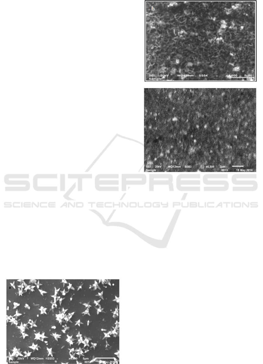
3.1 Morphological Proprieties
Fig. 1 shows the SEM surface images of Cd
x
Zn
1-x
S
thin films of composition x= 0.7, 0.5, 0.1,
respectively. As the composition (x) increases Zn is
more incorporated into CdS films. Which are
indicated by XRD as well as SEM (S.V. Borse, 2007).
The CdZnS layer constituted of a dense layer of small
crystallites and few large particles are embedding in
the surface. These particles are quite likely Cd
x
Zn
1-x
S
colloidal particles formed on the substrate during film
growth. The shape of particle is changing with
increases of Zn concentration.
Fig. 1 Typical SEM images of nanostructured
Cd
x
Zn
1-x
S thin films (a=Cd
0.1
Zn
0.9
S, b= Cd
0.5
Zn
0.5
S,
c= Cd
0.7
Zn
0.3
S) annealed at 500 °C.
3.2 Optical Properties
The optical transmission of CdZnS thin films with
different concentrations is using the
Spectrophotometer UV-visible (Shimadzu UV-
1800). We observe that the transmittance of our
samples is varied between 60 and 80% in visible
region this variation due to the decrease in Zinc
concentration. Whereas in the region <450 nm
fundamental absorption therefore, our thin films
possess transparency performance in the 450-800 nm
region, the latter gives them great importance in solar
cells as a buffer layer.
ICCSRE 2018 - International Conference of Computer Science and Renewable Energies
32
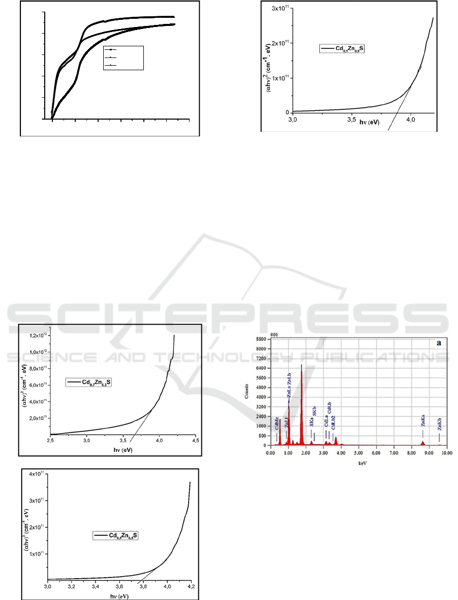
Fig. 2 Transmission spectra of Cd
x
Zn
1-x
S thin films.
The optical band gap Eg was obtained by
extrapolating the linear portion of the plot (αhν)
2
versus (hν) to α = 0, according to the following
equation (Y. Bakha, 2011):
α = A (hν − Eg)
n
(1)
Where hν is the photon energy, Eg is the band gap, A
is the edge parameter and n = 1/2 for direct gap
material.
The values of optical band gap Eg of thin films
(Cd
0.7
Zn
0.3
S, Cd
0.5
Zn
0.5
S and Cd
0.1
Zn
0.9
S) are (3.5,
3.61 and 3.8 eV) respectively, we find that the gap
energies of our thin layers are closer to that of ZnS
(K. Nagamani, 2012, T. Ben Nasr 2006).
Fig. 3 Extrapolations of E
g
for Cd
x
Zn
1-x
S thin films.
3.3 Chemical Composition
Quantitative analysis by EDX mines layers of CdZnS
was carrying out to investigate the stoichiometry. The
results are present Fig.4, which confirms the presence
of Cd, Zn and S, with atomic percentages of Cd / Zn
/ S: 19.36 /60.43 /20.20, 42.69/19.08/38.23 and
40.41/23.35/36.23 for three concentrations of
Cd
0.1
Zn
0.9
S, Cd
0.7
Zn
0.3
S, and Cd
0.5
Zn
0.5
S (A.
Abdolahzadeh Ziabari, 2013), (] S.D. Chavhan,
2008).
300 450 600 750 900 1050 1200
0
20
40
60
80
100
Cd
0.7
Zn
0.3
S
Cd
0.5
Zn
0.5
S
Cd
0.1
Zn
0.9
S
Intensity (u.a)
Wavelength (nm)
Zinc Doped of CdS Layers Deposited by Chemical Bath Deposition Method
33
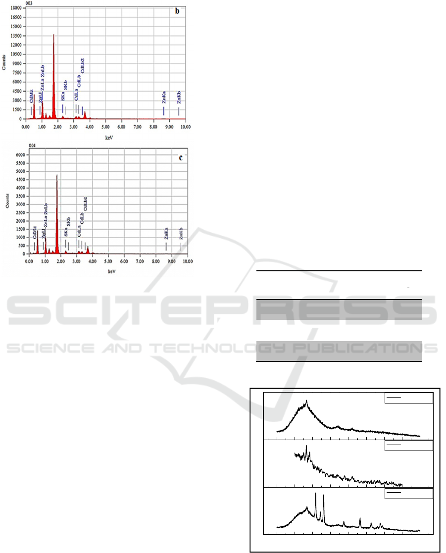
Fig. 4 EDX spectra for CdZnS thin films (a
=Cd
0.1
Zn
0.9
S, b= Cd
0.7
Zn
0.3
S, c= Cd
0.5
Zn
0.5
S)
3.4 Structural Proprieties
X-ray diffraction (XRD) spectra give information on
the nature of structure and the composition of a thin
film. These XRD diagrams confirm the formation and
composition of the alloys of the ternary system
Cd
x
Zn
1-x
S with x = (0.1, 0.5, 0.7) are present in FIG.
5 Peaks: (100), (002), (101), (110), (103), (200) and
(201) correspond to the hexagonal structure of the
thin films of Cd
0.7
Zn
0.3
S and Cd
0.5
Zn
0.5
S (ASTM
JCPDS File No. 491302 and 241136). The peak (002)
is the most intense for Cd
0.7
Zn
0.3
S and Cd
0.5
Zn
0.5
S.
But for Cd
0.1
Zn
0.9
S the peaks are (111), (200), (210),
(211), (300), (222), (321) and (400), the most intense
peak is (200) correspond to the cubic structure
(JCPDS file No. 079-6257 and 6259 of ASTM). The
average size of the crystallites of CdZnS estimated
according to the formula of Debye-Scherer’s [23].
0.9/2 (2)
Where D is the crystallite size, λ = 0.154 nm the mean
wavelength of Cu Kα radiation and β = (Δ2θ) is the
full-width half maximum (FWHM) of Bragg peak
observed at Bragg angle θ (rad), K = 0.9, the values
of D obtained. The grain size values, of Cd
x
Zn
1-x
S
thin layers deposited at bath temperature 80 ± 5 ° C
and annealed at 500 ° C are shown in Table 1. From
the table it can be seen that the size of the crystallites
increases with increasing zinc compositions (x) (R.
Mariappan, 2011).
The lattice parameter values were calculated using the
formula (3) and (4):
1/
2
= 4/3 ((
2
+ +
2
)/
2
) +
2
/
2
(3)
1/
2
= (
2
+
2
+
2
)/
2
(4)
Moreover, the obtained values are compiled in Table
1 (D. Patidar, 2008), the lattice parameter is decreased
when the zinc concentration increases, when the zinc
concentration is greater than 0.5 M the crystal
structure changes from hexagonal to cubic.
Tab.1 XRD results of CdZnS thin films.
(hkl) D
(nm)
Lattice parameter Å
Cd
0.7
Zn
0.3
S
(002) 9.95 c= 6.62, a= 4.08
Cd
0.5
Zn
0.5
S
(002) 20.66 c= 6.42, a= 3.95
Cd
0.1
Zn
0.9
S
(200) 25.82 a= 5.73
Fig. 5 XRD pattern of Cd
x
Zn
1-x
S thin films.
10 20 30 40 50 60 70 80 90
2
Cd
0,1
Zn
0,9
S
C (111)
C(200)
C (210)
C(211)
C(300)
C (222)
C (321)
C(400)
Intensity (a. u.)
Cd
0,5
Zn
0,5
S
H (100)
H(002)
(101)
H (110)
H (103)
H (201)
Cd
0,7
Zn
0,3
S
H (002)
H (110)
H (200)
ICCSRE 2018 - International Conference of Computer Science and Renewable Energies
34

4 CONCLUSIONS
Synthesis CdZnS thin films by chemical bath
deposition (CBD) were easy and feasible for
deposition on large-area glass substrates. The study
of the characterizations showed that the morphology
of the surface and the transmittance are modified with
respect to the zinc concentration. The energy of the
interval is of the order of 3.5 to 3.8 eV. The crystalline
structure is hexagonal for (Cd
0.7
Zn
0.3
S and
Cd
0.5
Zn
0.5
S) and cubic for Cd
0.1
Zn
0.9
S. and the grain
size is between 9.95 and 25 nm.
REFERENCES
T. Gruszecki, B. Holmstrom, Sol. Energy Mater. Sol.
Cells31 (1993) 227–234.
D. Xia, T. Caijuan, T. Rongzne, L. Wei, F. Lianghuan, Z.
Jingquan, W. Lili, L. Zhi, J. Semicond.32 (2011)
22003.
T.D. Dzhafarov, F. Ongul, I. Karabay, J. Phys. D Appl.
Phys. 39 (2006) 3221.
T. Prem Kumar, S. Sarvana Kumar, K. Sankaranarayanan,
Appl. Surf. Sci. 257(2011) 1923–1927.
Ng. Gaewdang, T. Gaewdang, Materials Letters 59 (2005)
3577 – 3584.
A. Mukherjee, M. Fu, P. Mitra, Journal of Physics and
Chemistry of Solids 82(2015)50–55.
R. Mariappan, M. Ragavendar, V. Ponnuswamy, J. Alloys
Compd. 509 (2011)7337–7343.
P.B. Bagdare, S.B. Patil, A.K. Singh, J. Alloys Compd.
506(2010) 120–124.
Y. Ravi Prakash, K.V. Bangera, G.K. Shivakumar, Growth,
Appl. Phys. 10 (2010) 193–198.
M. Glatettin Baykul, Nilgun orhan, Thin Solid Films 518
(2010) 1925–1928.
G. Laukaitish, S. Lindroos, S. Tamulevicius, M. Leskela,
M. Rackaitis, Appl. Surf. Sci. 161 (2000) 396–405.
D. Patidar, N.S. Saxena, T.P. Sharma, J. Mod. Opt. 55
(2008) 79–88.
P. Kumar, A. Misra, D. Kumar, N. Dhama, T.P. Sharma,
P.N. Dixit, Opt. Mater. 27 (2004) 261–264.
M. Abdel Rafea, A.A.M. Farag, N. Roushdy, J. Alloys
Compd. 485 (2009) 660–666.
V. Kumar, S.K. Sharma, D.K. Dwivedi, J. Alloys Compd.
512 (2012) 351–354.
R. Zellagui, H. Dehdouh, F. Boufelgha, A. Boughelout, T.
Sahraoui, D. Chaumont, M. Adnane, Effect of
zinc/cadmium proportion in CdS layers deposited by
CBD method, International Multidisciplinary Research
Journal 2019, 9: 8-12.
S.V. Borse, S.D. Chavhan, Rampha Sharma, Journal of
Alloys and Compounds 436 (2007) 407–414
Y. Bakha, K.M. Bendimerad, and S. Hamzaoui, Eur. Phys.
J. Appl. Phys. 55, 30103 (2011)
K. Nagamani, N. Revathi, P. Prathap, Y. Lingappa, K.T.
Ramakrishna Reddy, Current Applied Physics 12
(2012) 380-384
T. Ben Nasr, N. Kamoun, M. Kanzari, R. Bennaceur, Thin
Solid Films 500 (2006) 4 – 8.
A. Abdolahzadeh Ziabari, F.E.Ghodsi, Materials Science
in Semiconductor Processing 16 (2013) 1629–1636.
S.D. Chavhan, S. Senthilarasu, Soo-Hyoung Lee, Applied
Surface Science 254 (2008) 4539–4545.
D. PATIDAR , N. S. SAXENA, T. P. SHARMA, Journal
of Modern Optics, Vol. 55, No. 1, January 10, 2008, 79-
88
.
Zinc Doped of CdS Layers Deposited by Chemical Bath Deposition Method
35
