
Characterization of a Single Layer of Si
0.73
Ge
0.27
and a
Quantum-well Structure of Si
0.4
Ge
0.6
/Ge by Quantitative
SIMS Depth Profiling Using the Analytical Depth Resolution
Function of the MRI Model
Q R Deng, H L Kang, Y S Han, X H Zhang, X W Mai, Q Q Huang and J Y
Wang
*
Department of Physics, Shantou University, 243 Daxue Road, Shantou, 515063
Guangdong, China
Corresponding author and e-mail: J Y Wang, wangjy@stu.edu.cn
Abstract. The analytical depth resolution function of the Mixing-Roughness-Information
(MRI) model is used to fit the measured SIMS depth profiling data of a single layer of
Si
0.73
Ge
0.27
and a Si
0.4
Ge
0.6
/Ge quantum-well structure on Si substrate. The interface
roughness and the individual layer thickness and the depth resolution values are determined
accordingly. The obtained layer thickness values in Si
0.4
Ge
0.6
/Ge quantum-well structure are
consistent with the ones measured by HR-TEM with a maximum relative error less than
1.2%.
1. Introduction
Quantum-well structures with layer thickness in the range of a few nm or tens of nm have been
widely used for micro-electronic devices [1]. The performance of device depends strongly on the
quality of the quantum-well structure. In particular, the variations of layer thickness and interface
roughness may have a significant influence on the function of device [2]. The layer thickness in a few
nm range is conventionally measured by HR-TEM, which involves the complex procedures of
sample preparation and measurement. On the other hand, quantitative SIMS depth profiling may
provide an alternative way to determine the layered structure with one nm resolution. Recently, with
the development of the advanced SIMS instrument, the artifacts that present often in any depth
profiling, such as sputtering induced roughness, crater effect and matrix effect, have been
significantly minimized and the HR-SIMS depth profile could be simply obtained. In this paper, it
will be demonstrated that not only could the quantum-well structure and the depth resolution but also
the interface roughness be well determined by fitting the measured SIMS depth profiling data using
the analytical depth resolution function of the MRI model.
2. Analytical depth resolution function of the MRI model
The measured depth profiles differ from the true concentration-depth profiles as a result of various
interactions of the ion beam bombardment with the measured sample, e.g. ion implantation, cascade
mixing, etc. A so-called depth resolution function (DRF) is often used to describe the distortion of
486
Deng, Q., Kang, H., Han, Y., Zhang, X., Mai, X., Huang, Q. and Wang, J.
Characterization of a Single Layer of Si0.73Ge0.27 and a Quantum-Well Structure of Si0.4Ge0.6/Ge by Quantitative SIMS Depth Profiling Using the Analytical Depth Resolution Function of
the MRI Model.
In Proceedings of the International Workshop on Materials, Chemistry and Engineering (IWMCE 2018), pages 486-492
ISBN: 978-989-758-346-9
Copyright © 2018 by SCITEPRESS – Science and Technology Publications, Lda. All rights reserved

the measured depth profiles as compared to the true ones, which causes the depth profiles
degradation in the physical mechanism. Generally speaking, in sputter depth profiling, the measured
and normalized intensity I(z)/Io can be described as the convolution of the true concentration X(z') at
the original depth z' in the sample with a DRF g(z-z') as [3]:
0
0
()
(')( ') '
Iz
X
zgz zdz
I
∞
=−
∫
(1)
Where z' is the running depth parameter for which the composition is defined and z is the
sputtered depth. With the measured and normalized intensity I(z)/Io and a known DRF g(z-z'), the
true in-depth distribution of composition can be calculated by Eq. (1). Therefore, the exact
knowledge of the DRF is the key to accurate reconstruction of the original depth distribution of the
composition from the measured depth profile [4]. In the MRI model, the DRF g(z-z') takes into
account the three physically meaningful effects in any sputtering depth profiling: atomic mixing,
surface/interface roughness, Information depth, which are described, respectively , by [5]:
Mixing length (w):
()
'
1
(')exp
w
zz w
gzz
ww
−−+
⎡
⎤
−=
⎢
⎥
⎣
⎦
(2)
Roughness (σ):
2
2
1(')
(') exp
2
2
zz
gzz
σ
σ
πσ
⎡
⎤
−−
−=
⎢
⎥
⎣
⎦
(3)
I
nformation depth (λ):
()
'
1
(')exp
zz
gzz
λ
λλ
−−
⎡
⎤
−=
⎢
⎥
⎣
⎦
(4)
Where w is the atomic mixing length, σ is the surface/interface roughness and λ is the information
depth parameter. With the above three partial resolution functions, the DRF g(z-z') can be written as:
(') (') (') (')
w
gz z g z z g z z g z z
σλ
−= −⊗ −⊗ −
(5)
In general, the quantitative results of the MRI model are obtained by the numerical solution of the
convolution integral with combining Eq. (1) and Eq. (5).
With respect to the above-discussed refinements of the DRF in terms of symmetric (Gaussian
functions) and asymmetric (non-Gaussian functions) functions, it is necessary to clarify the
contribution to the depth resolution △z (16-84%). According to the MRI model, three physically
meaningful effects contribute to the depth resolution function. A symmetric contribution to the depth
resolution function originates from the intrinsic roughness and the surface roughening by ion
sputtering, which both are described by a Gaussian smearing function (see Eq. (3)), characterized by
its standard deviation of the surface roughness parameter σ. For the asymmetric broadening
functions, the atomic mixing is described by an exponential function (see Eq. (2)), characterized by
the atomic mixing length w; the information depth of the Auger electrons (for AES) is also described
by an exponential function (see Eq. (4)), characterized by the information depth λ. Hence, on the
basis of the three MRI parameters, the total depth resolution can approximately be rewritten as [6]
()( )
1/2
22
2
2 1.668 (1.668 )zw
σλ
⎡⎤
Δ= + +
⎣⎦
(6)
Characterization of a Single Layer of Si0.73Ge0.27 and a Quantum-Well Structure of Si0.4Ge0.6/Ge by Quantitative SIMS Depth Profiling
Using the Analytical Depth Resolution Function of the MRI Model
487
Fitting the experimental depth profile by the MRI model leads to obtain the values of σ, w and λ.
Then, the depth resolution △z can be calculated with Eq. (6).
2.1. Analytical solution for delta layer
For the special case of being an ideal delta function with vanishing thickness, an analytical
resolution function can be derived with the result I(z)/I
0
=g
△MRI
by Eq. (1) given by [7]
()
⎥
⎦
⎤
⎢
⎣
⎡
⎟
⎟
⎠
⎞
⎜
⎜
⎝
⎛
−
−−
+×
⎪
⎭
⎪
⎬
⎫
⎪
⎩
⎪
⎨
⎧
⎥
⎥
⎦
⎤
⎢
⎢
⎣
⎡
⎟
⎟
⎠
⎞
⎜
⎜
⎝
⎛
++
⎪
⎭
⎪
⎬
⎫
⎪
⎩
⎪
⎨
⎧
⎥
⎦
⎤
⎢
⎣
⎡
+
⎟
⎟
⎠
⎞
⎜
⎜
⎝
⎛
−−
−×
⎪
⎭
⎪
⎬
⎫
⎪
⎩
⎪
⎨
⎧
⎥
⎥
⎦
⎤
⎢
⎢
⎣
⎡
⎟
⎟
⎠
⎞
⎜
⎜
⎝
⎛
+
⎟
⎟
⎠
⎞
⎜
⎜
⎝
⎛
−−
⎥
⎦
⎤
⎢
⎣
⎡
⎟
⎟
⎠
⎞
⎜
⎜
⎝
⎛
−−=
Δ
λ
σ
σλ
σ
λλ
σ
σ
σ
λ
wz
erf
z
w
wz
erf
ww
wzw
w
zg
MRI
2
1
1
2
1
exp
2
1
2
1
1
2
1
expexp1
2
1
2
2
(7)
For SIMS, assuming that practically all of the detected ions stem from the first atomic layer, the
information depth parameter in the MRI model for SIMS can be set to zero. The DRF for MRI-SIMS
is given by
()
()
⎥
⎦
⎤
⎢
⎣
⎡
⎟
⎟
⎠
⎞
⎜
⎜
⎝
⎛
+
+
−−
⎥
⎥
⎦
⎤
⎢
⎢
⎣
⎡
⎟
⎟
⎠
⎞
⎜
⎜
⎝
⎛
+
+
−=
−Δ
w
wz
erf
ww
wz
w
zg
SIMSMRI
22
1
2
1
exp
2
1
2
σ
σ
σ
(8)
To demonstrate the behavior of the analytical resolution function of the MRI model for different
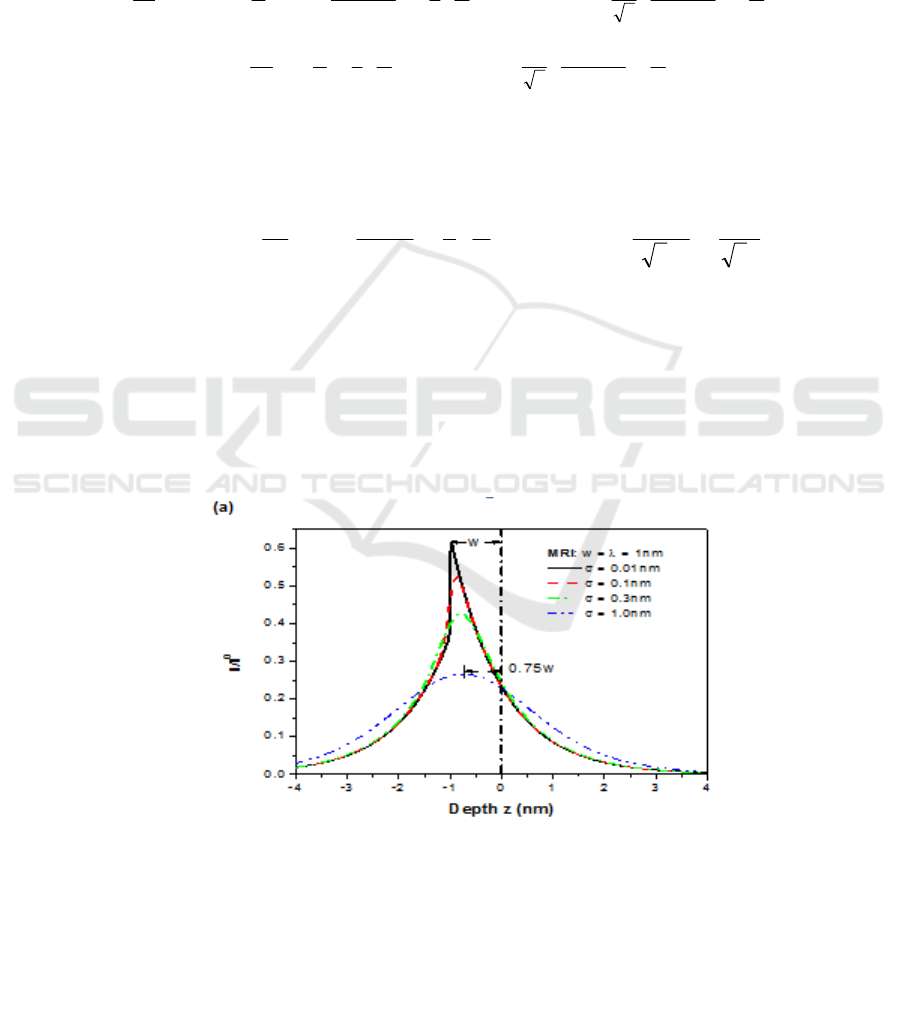
roughness, Figure 1. a shows a plot of Eq. (7) for w = λ = 1nm and σ = 0.01, 0.1, 0.3 and 1.0 nm. The
steep rise at z = z(0) -w is caused by the actual onset of complete mixing of the delta layer, with the
mixing zone length w governing the decay of the signal for z > z(0) -w. When the roughness
increases, this behavior is smoothed out because of the microscopically different spatial onsets of
mixing. [9] For increasing roughness, the maximum of the total DRF shifts from z = z(0) -w in the
direction of z = z(0), until it coincides with its centroid given by a combination of both exponential
functions for w and λ. [8]
Figure 1. Analytical depth resolution function of the MRI model (Eq. (7)) for w =λ = 1nm and
different roughness parameter values, σ = 0.01, 0.1, 0.3 and 1nm. Replotted from Ref [9].
2.2. Analytical solution for thick layer
As already proposed by Zalm [9] and later by Gautier et al.[10], including a term for layer thickness
appears to be possible in the analytical DRF. In the MRI model we can introduce a layer thickness d
= z
2
– z
1
, where z
1
denotes the beginning and z
2
the end of the layer. For SIMS (λÆ0), the DRF for a
layer with thickness of z
2
– z
1
is given by [8]
IWMCE 2018 - International Workshop on Materials, Chemistry and Engineering
488

12
0
2
2211
1
(()/ )
2
22
11
exp
22
exp 1 exp 1
22 22
dMRISIMS
zwz zwz
Iz I erf erf
zw
ww
z zwz z zwz
erf erf
ww
ww
σσ
σ
σσ
σσ
−−
⎡⎤
+− +−
⎛⎞⎛⎞
=−
⎢⎥
⎜⎟⎜⎟
⎝⎠⎝⎠
⎣⎦
⎡⎤
+
⎛⎞
+−+
⎢⎥
⎜⎟
⎝⎠
⎢⎥
⎣⎦
⎧ ⎫
⎡⎤⎡⎤
+− +−
⎛⎞ ⎛⎞
⎪ ⎪
⎛⎞ ⎛⎞
×+ −−+ −
⎨ ⎬
⎜⎟ ⎜⎟
⎢⎥⎢⎥
⎜⎟ ⎜⎟
⎝⎠ ⎝⎠
⎝⎠ ⎝⎠
⎪ ⎪
⎣⎦⎣⎦
⎩ ⎭
(9)
In SIMS, the simple analytical solution of the ideal delta layer is usually applied for monolayers.
In reality, however, the thinnest layer is an atomic monolayer, with a thickness of 0.25 ± 0.05 nm in
most semiconductors and metals. If we assume a DRF of lower limit, for example for the case of
SIMS (Eq. (9)) with σ = w = 1 ML, the resulting FWHM (full width at half maximum) of the profile
for z
2
- z
1
= 0 is about 2.9 monolayers or ca.0.8 nm for a delta layer [8]. It shows that the FWHM of
the measured profile after Eq. (9) increases slightly with increasing layer thickness until it becomes
identical to the latter for a thickness above 8 monolayers [8]. For higher values of the DRF
parameters the deviation between an ideal delta layer and a monolayer is reduced.
In summary, analytical DRFs can be applied to the convolution integral of (1) Delta layers, (2)
Layers with any finite thickness and constant analyte concentration, (3) Multilayers of type 2). [8]
The main advantage of the analytical solution of the DRF is that the application of it is simple and
user friendly because no computer programming is necessary for graphical representation. It is
particularly useful for quantifying measured delta layer depth profiles in AES and SIMS [11]. This
paper will demonstrate that the layer thickness and the depth resolution values could be obtained by
fitting the measured SIMS depth profiles of a multilayer (a quantum-well structure) and a thick layer
respectively by applying the analytical solution of the convolution integral. It is customary to assume
X(z) and to calculate the intensity I(z)/I
0
in a “forward” manner with a known depth resolution
function g(z), and compare it with the measured I/I
0
(z). This procedure is performed repeatedly by
trial and error until an optimum fit of both is obtained. This is done by a computational program that
varies the X(z) distribution until the minimal value of the average deviation of the calculated from
the measured profiles is achieved. The final input X(z) is the reconstructed, original in-depth
distribution of composition.
3. Results and discussion
To demonstrate the application of the analytical MRI model, the measured SIMS depth profiles of
Si
0.73
Ge
0.27
superficial layer and Si
0.4
Ge
0.6
/Ge 10-period quantum well (QW) on Si substrate [2, 12]
will be quantified. Both layer structures were deposited on Si substrate by chemical vapor deposition
(CVD). The Si
1−x
Ge
x
superficial layer thickness is determined as 26.6 ± 0.5nm [2]. The Si
0.4
Ge
0.6
/Ge
10-period QW thickness values determined from HR-XTEM picture are listed in Table 1 [12]. The
SIMS profiling was performed with an Atomika 4500 instrument using primary ions of O
2
+
with a
range of energies (0.25–1keV) at near normal incidence. An area of 220x220 mm was scanned, and
the 30Si
+
and 70Ge
+
secondary ions were recorded.
Table 1. Si
0.4
Ge
0.6
/Ge QW thickness values determined by XTEM [12].
Figure 2 shows the measured and normalized Ge SIMS depth profiles as open circles for
Si
0.73
Ge
0.27
superficial layer on Si substrate using different O
2
+
beam energies from 0.4-2.0 keV. The
best fits for each measured depth profile using Eq. (9) are shown as solid lines in Figure 2. The
Period number 1 2 3 4 5 6 7 8 9 10
Si0.4Ge0.6 layer (nm) 8.6 8.6 8.6 8.5 8.5 8.5 8.4 8.5 8.4 8.6
Ge layer (nm) 12.6 12.7 12.6 12.6 12.7 12.7 12.7 12.7 13.0 12.8
Characterization of a Single Layer of Si0.73Ge0.27 and a Quantum-Well Structure of Si0.4Ge0.6/Ge by Quantitative SIMS Depth Profiling
Using the Analytical Depth Resolution Function of the MRI Model
489
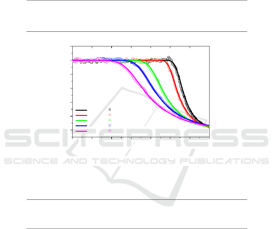
corresponding MRI parameters are listed in Table 1 together with the depth resolution values
calculated from Eq. 6. It shows clearly that upon increasing the O
2
+
beam energy, the atomic mixing
length increases from 1.1nm to 3.0nm and the roughness parameter increases from 0.4 nm to 1.0 nm,
yielded the increasing of depth resolution, i.e. the degradation of measured depth profile.
Table 2. The best fits of the MRI parameter and the corresponding depth resolution values.
400 eV 500 eV 1keV 1.5 keV 2 keV
w (nm) 1.1 1.3 2.0 2.6 3.0
σ (nm) 0.4 0.4 0.7 0.8 1.0
Depth resolution (nm) 2.0 2.3 3.6 4.7 5.4
16 18 20 22 24 26 28 30
0.0
0.2
0.4
0.6
0.8
1.0
1.2
400eV
500eV
1keV
1.5keV
2keV
400eV
500eV
1keV
1.5keV
2keV
Exp.data
MRI fitting
Normalized intensity
Depth (nm)
Figure 2. The measured SIMS profiles (open circles) [2] and the fitted profiles (solid lines) using the
MRI analytical depth resolution function.
Table 3. The best fits of the MRI parameter and sputtering rate values.
250 eV 500 eV
w (nm) 0.9 0.1
σ (nm) 1.2 1.2
Sputtering rate (nm/s)
0.01 0.03
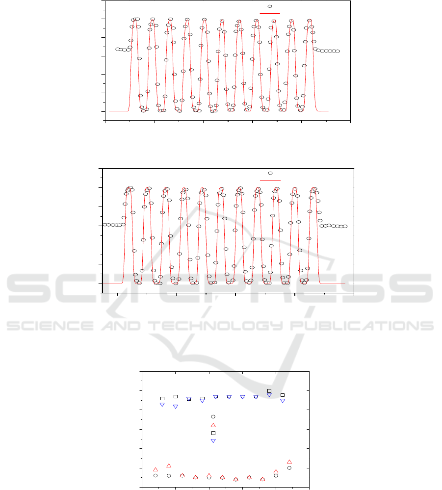
Figure 3 shows the measured and normalized Si SIMS depth profiles as open circles for
Si
0.4
Ge
0.6
/Ge 10-period QW structure on Si substrate using (a) 250 eV and (b) 500eV O
2
+
beam
energy sputtering. The best fits for the measured depth profiles using Eq. (9) are shown as solid lines
in the respective figure. The corresponding MRI parameters are listed in Table 2 together with the
average sputtering rate of Si
0.4
Ge
0.6
layer. Both the MRI fits are based on the same QW layered
structure that is taken as one of fitting parameters. The fitted individual layer thickness of each period
is shown by different symbols in Figure 4 and is compared with the value listed in Table 1. The
maximum relative error between the fitted thickness and the one obtained by XTEM is less than
1.2%. This implies that the quantitative SIMS depth profiling can provide an alternative way for
determination of nano-layered structure. Meanwhile, the fitted interface roughness of 1.2 nm in
Si
0.4
Ge
0.6
/Ge QW structure is slight higher than that of 0.4 nm in Si
0.73
Ge
0.27
superficial layer on Si
substrate. This implies that both samples prepared by CVD are very smooth.
IWMCE 2018 - International Workshop on Materials, Chemistry and Engineering
490
5000 10000 15000 20000 25000 30000
0.0
0.2
0.4
0.6
0.8
1.0
1.2
(a)
No r malized i ntensity
Sputting time(s)
Experiment Data
MRI fitting
2000 4000 6000 8000 10000
0.0
0.2
0.4
0.6
0.8
1.0
1.2
(b)
Experiment Data
MRI fitting
No r mali ze intensity
Sputting time(s)
Figure 3. SIMS depth profiles [12] of Si (open circles) (a) 250 eV and (b) 500eV O
2
+
and MRI fitted
profiles (solid lines) for Si
0.4
Ge
0.6
/Ge QW structure.
0 5 10 15 20 25
8
9
10
11
12
13
14
layer numbers in Si
1-x
Ge
x
/Ge QW
XTEM Si
1-x
Ge
x
layer thickness
MRI fitting
XTEM Ge layer thicknes
MRI fitting
relative error
:
1.2%
layer thickness (nm)
Figure 4. Comparison of the fitted and the measured (listed in Table 1) layer thickness values of
Si
0.4
Ge
0.6
and Ge sublayers in Si
0.4
Ge
0.6
/Ge QW structure.
4. Conclusions
The analytical DRF of the MRI model that is simple and user friendly has successfully been used to
quantify the measured SIMS depth profiling data of nano-layered structures. The individual layer
Characterization of a Single Layer of Si0.73Ge0.27 and a Quantum-Well Structure of Si0.4Ge0.6/Ge by Quantitative SIMS Depth Profiling
Using the Analytical Depth Resolution Function of the MRI Model
491

thickness, the interface roughness and the depth resolution values are determined accordingly. The
extracted layer thickness values for Si
0.4
Ge
0.6
/Ge quantum-well structure are consistent with the ones
determined by XTEM.
References
[1] Kang Y, Han-Din L, Morse M, Paniccia M J, Zadak M, Litski S, Sarid G, Pauchard A, Y H
Kuo, H W Chen, Zaoui W S, Bowers J E, Beling A, McIntosh D C, X Zheng and
Campbell J C 2009 Nature Photonics 3 59–63
[2] Dowsett M G, Morris R J H, Hand M and et al 2011 The influence of beam energy on apparent
layer thickness ultralow energy O2+ SIMS on surface Sil-xGex J. Surf. Interface Anal
43(1-2) 211-213
[3] Ho P S and Lewis H E 1976 Deconvolution method for composition profiling by Auger
sputtering technique Surf. Sci. 55 335–348
[4] Hofmann S 1998 Sputter depth profile analysis of interfaces Rep. Prog. Phys. 61 827–888
[5] Hofmann S 1994 Atomic mixing, surface roughness and information depth in high-resolution
AES depth profiling of a GaAs/AlAs superlattice structure J. Surf. Interface Anal. 21(9)
673-678
[6] Wang J Y, Starke U and Mittemeijer E J 2009 Evaluation of the depth resolutions of Auger
electron spectroscopic, X-ray photoelectron spectroscopic and time-of-flight secondary-ion
mass spectrometric sputter depth profiling techniques Thin Solid Films.517 3402–3407
[7] Liu Y, Hofmann S and Wang J Y 2013 An analytical depth resolution function for the MRI
model, Surf. Interface Anal. 45 1659-1660
[8] Hofmann S, Liu Y, Wang J Y and et al. 2014 Analytical and numerical depth resolution
functions in sputter profiling J. Appl. Surf. Sci. 314 942-955
[9] Zalm P C 1995 Ultra shallow doping profiling with SIMS Rep. Prog. Phys. 58 1321-1373
[10] Gautier B, Prost R, Prudon G and Dupuy J C 1996 Deconvolution of SIMS depth profiles of
Boron in Silicon Surf. Interface Anal. 24 733-745
[11] Kang H L, Lao J B, Li Z P and et al 2016 Reconstruction of GaAs/AlAs superlattice multilayer
structure by quantification of AES and SIMS sputter depth profile Applied Surface Science
38 584-588
[12] Morris R J H, Dowsett M G, Beanland R and et al 2013 O2+ probe-sample conditions for
ultralow energy SIMS depth profiling of nanometre scale Si
0.4
Ge
0.6
/Ge quantum wells J.
Surf. Interface Anal. 45(1) 348-351
IWMCE 2018 - International Workshop on Materials, Chemistry and Engineering
492
