
Research on NiCoB Diffusion Barrier Film Prepared by
Electroless Deposition for ULSI-Cu Metallization
Z H Yang
1
, X H Chen
1, *
, W H Ma
2
, Y C Wang
1
, K Chen
3
and J X Han
1
1
Institution of Materials Science and Engineering, Yunnan University, Kunming,
China
2
National Engineering Laboratory of Vacuum Metallurgy, Kunming University of
Science and Technology, Kunming, China
3
Institution of Physics and Astronomy, Yunnan University, Kunming, China
Corresponding author and e-mail address: X H Chen, chenxh@ynu.edu.cn
Abstract. In this paper, NiCoB/Cu/NiCoB/Si and NiCoB/Si samples were prepared by
electroless deposition. XPS, XRD, FPP and AFM were used to characterize the elemental
valence and composition, phases, sheet resistance and surface morphology of the samples.
According to the results, it can be found that the electroless deposited NiCoB film was
amorphous, and it was composed of CoB compound and elementary Ni. The results of NiCoB
films annealed at temperatures ranging from 500°C to 850°C demonstrated that the
electroless deposited NiCoB film can block Cu diffusion effectively until 850°C.
1. Introduction
Admittedly, the resistance-capacitance delay of a circuit has become the limiting factor in the speed
of device with the decrease in the minimum feature size of ultra-large scale integration [1-4]. In order
to resolve the crisis caused by the interconnection delay, Cu has been applied as the interconnect
material due to its low resistivity and high resistance to electromigration [5-8]. However, there must
be an ideal barrier layer between Cu and Si due to the poor adhesion of Cu as well as the diffusion
between Cu and Si [9].
Owing to the high melting point, small contact resistance, low stress and excellent
thermostability, Ti alloy and Ta alloy became the most widely used diffusion barrier materials in Cu
metallization as well as in Al based metallization [10-13]. Recently, with the continuous
improvement of integration, traditional Ti alloy and Ta alloy barrier layers were no longer qualified
for the job in terms of the film thickness, thermostability, electrical conductivity and uniformity.
Besides, it is an arduous task to explore barrier layer materials with superior performance.
In comparison with other physical and chemical vapor deposition methods, electroless deposition
is a promising technique because of the relative low temperature, low cost, low defect density, high
uniformity and conformality [14-16]. In most cases, electroless deposition of diffusion barrier
materials concentrated in cobalt and nickel based alloys [17, 18]. Sung-Te Chen [19] etc. studied the
Co-P barrier film and found that the Co-P barrier layer not only acted as catalysts for the electroless
deposition of the copper film, but also increased the thermostability of the Cu metallization layer.
Hila Einati [20] et al. found that the Co-W-B film with 2.2 at% boron revealed the high resistance to
Yang, Z., Chen, X., Ma, W., Wang, Y., Chen, K. and Han, J.
Research on NiCoB Diffusion Barrier Film Prepared by Electroless Deposition for ULSI-Cu Metallization.
In Proceedings of the International Workshop on Materials, Chemistry and Engineering (IWMCE 2018), pages 425-433
ISBN: 978-989-758-346-9
Copyright © 2018 by SCITEPRESS – Science and Technology Publications, Lda. All rights reserved
425

air oxidation. S.M.S.I. Dulal [21] etc invented an alkali-metal-free bath for electroless deposition of
Co-W-P film for copper interconnections. A. Kohn [15] et al. pointed out that the increase of W
degraded the quality of Co-W-P alloy film. Anuj Kumar [22] etc discovered the Ni-Co-P film, with
lower Co and higher P contents can prevent the diffusion of Cu until 500 °C. N-dimethyl amine
borane (DMAB) can be used as reducing agent in electroless Ni, Ni baths with DMAB can work in
both acid and alkaline baths, and the overall reduction reactions produce metallic nickel or nickel
boride [23]. DMAB can reduce Ni
2+
and Co
2+
from solution at the same time to co-deposit Ni-Co-B
alloy [24]. Besides, Ni-Co-B film possesses excellent magnetic property and corrosion resistance
[25-27], it has been widely used in the thin magnetic recording media and catalysis material [25, 28],
yet few studies have been conducted on the NiCoB barrier layer film on Cu interconnection. As a
result, it is a great interest to investigate how a NiCoB alloy film can be used as a diffusion barrier
layer on Cu interconnections.
In this study, NiCoB films were deposited as a barrier layer against Cu diffusion based on the
above mentioned electroless technique. NiCoB/Si and NiCoB/Cu/NiCoB/Si samples were prepared
and researched in order to obtain the NiCoB film with excellent barrier property.
2. Experimental
The substrates used in this study were single crystal n-type (100) silicon with the resistivity of 1~10
·cm. Prior to electroless deposition, the Si substrates were pre-treated as follows. At first, the wafer
was ultrasonically cleaned for 20 min in absolute alcohol. Then, it was treated a second time in an
ultrasonic assisted bath containing a roughening solution (4% H
2
SO
4
+ 5% H
2
O
2
) for 20 min
followed a sensitization process for 5 min in SnCl
2
+HCl solution (20 g/l SnCl
2
·2H
2
O + 40 ml/l HCl).
The cleaned wafer was subjected to ultrasonic treatment for 20 min in palladium activating solution
(0.25 g/l PdCl
2
+ 10 ml/l HCl + 3.2 g/l SnCl
2
·2H
2
O + 0.5 g/l Na
2
SnO
3
·3H
2
O
+ 250 g/l NaCl + 50 g/l
urea). Finally, it is the peptization process for 40 s in 10% HCl solution in a 45°C water bath.
Electroless deposition was conducted immediately after the pretreatment of Si substrates. The
experimental condition and composition of NiCoB as well as Cu plating baths are given in Table 1.
Deposition time for the first film (NiCoB), the second film (Cu) and the third film (NiCoB) was 5
min, 2 min, 30 s respectively. In addition, the deposition time for the single NiCoB film was also 5
min.
NiCoB/Si and NiCoB/Cu/NiCoB/Si samples were annealed at 500°C ~850 °C for 30 min in an
argon atmosphere. XPS, XRD, FPP and AFM were used to characterize the elemental valence and
composition, phases, sheet resistance and surface morphology of these samples before and after
annealing.
3. Results and Discussion
The thickness of films was measured by the SGC-10 film thickness gauge, the first film (NiCoB
barrier layer) is 40 nm, the second film (Cu) was 20 nm and the third film (NiCoB) was 50 nm. The
other characterizations of the deposited NiCoB/Si and NiCoB/Cu/NiCoB/Si samples are given as
follows.
3.1. Analysis of elemental valence state and composition
The elemental valence of the NiCoB film was determined from the element spectra as shown in
Figure1.
As shown the Figure 1(a), the bonding of Ni emerged at 869.93 eV and 852.60 eV respectively,
indicating that Ni element existed in the form of elementary Ni in the electroless deposited NiCoB
film. In addition, the bonding of Ni-O appeared at 879.30 eV, 873.60 eV, 861.00 eV and 855.80 eV,
which corresponds to NiO, indicating that a small amount of NiCoB film on the surface has been
oxidized.
IWMCE 2018 - International Workshop on Materials, Chemistry and Engineering
426
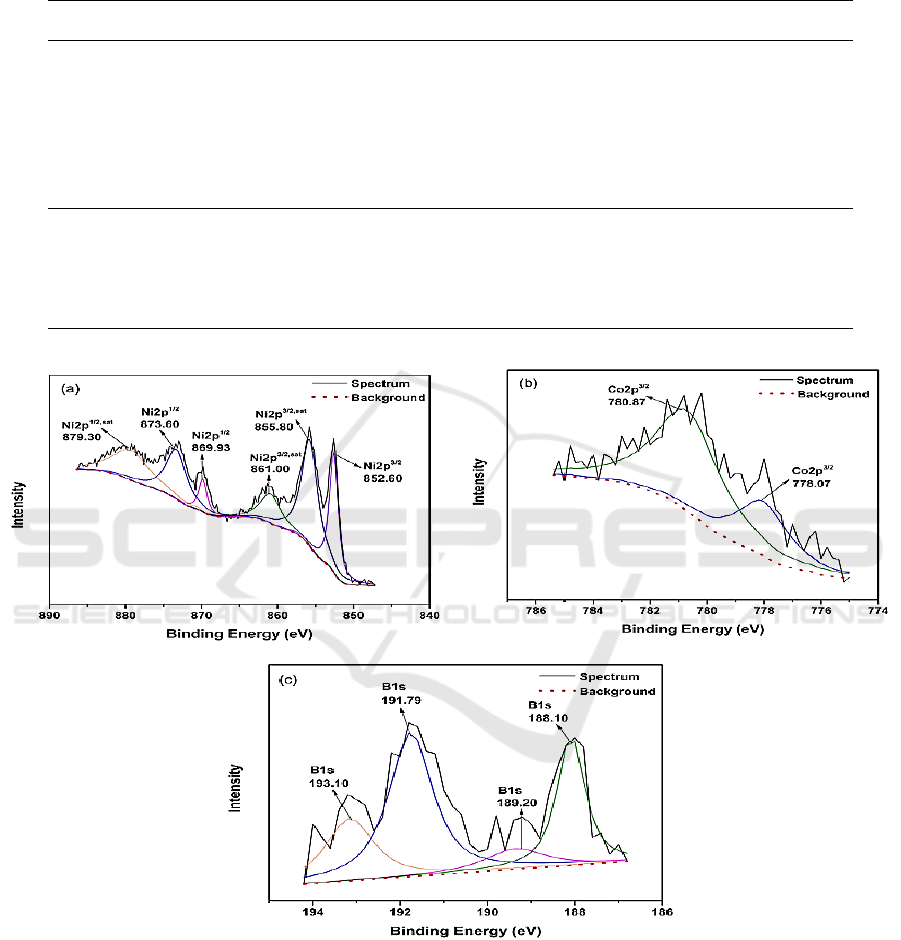
Table 1. Experimental conditions and composition of the plating baths for electroless deposition of
NiCoB and Cu.
Sample names Concentration (g/l) Operating conditions
NiC
oB
N
a
3
C
6
H
5
O
7·
2H
2
O 41.17
pH: 11
Temperature: 85 °C
C
4
H
4
O
6
KNa·4H
2
O 14.11
N
iSO
4
·6H
2
O 28.91
CoSO
4
·7H
2
O 8.43
DMAB(C
2
H
10
BN) 2.35
CH
3
COONa·3H
2
O 15
N
H
4
F 1.0
Cu
CuSO
4
·5H
2
O 20
pH: 12
Temperature: 77.5 °C
EDTA-2Na 39
CHOCOOH·H
2
O 13.8
C
6
H
8
O
7
·H
2
O 21
-’ bip
y
ridine (C
10
H
8
N
2
)0.01
Figure 1. Element spectra of Ni2p (a), Co2p (b) and B1s (c).
In the Co2p spectrum, the bonding of Co-O and Co-B appeared at the 780.87 eV and 778.07 eV,
the corresponding substances were CoO and CoB. It can be inferred that the Co element in the
electroless deposited NiCoB film primarily existed in CoB. Figure 1(c) is the spectrum of B1s, in
which the bonding of Co-B can be observed at 188.10 eV. In addition, a B
6
O peak (189.20 eV) and
B
2
O
3
peaks (193.10 eV, 191.79 eV) emerged, which resulted from the oxidation of the exterior
Research on NiCoB Diffusion Barrier Film Prepared by Electroless Deposition for ULSI-Cu Metallization
427
NiCoB film. XPS analysis demonstrated that the electroless deposited NiCoB film was mainly
composed of CoB compound and elementary Ni.
3.2. Analysis of phase
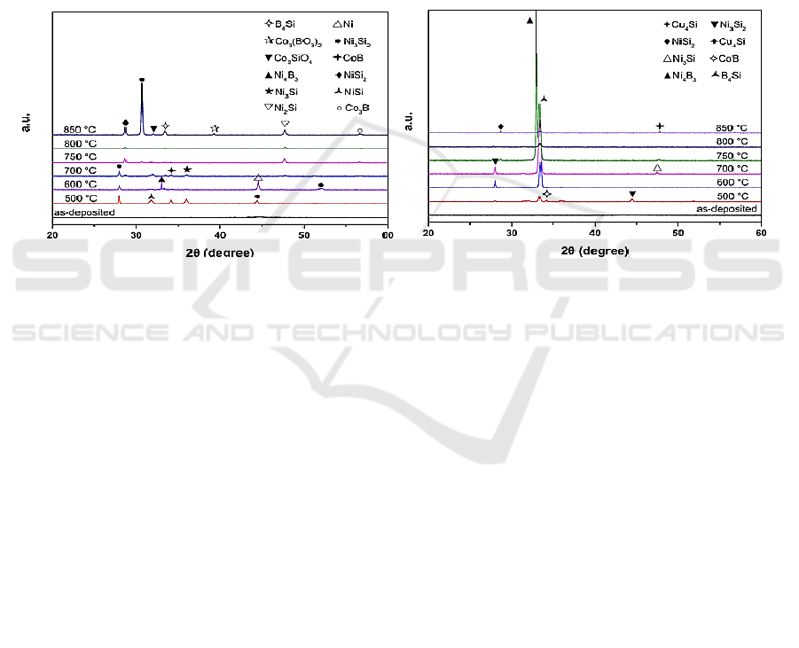
Figure 2 shows the XRD patterns of NiCoB/Si before and after annealing at 500 °C~850 °C. As
show this figure, the unannealed samples were almost amorphous. After annealing the film from 500
°C to 800°C, the film was crystallized and there were some new phases formed and disappeared
constantly. Annealing the film at 850 °C, phase species of the film were much more than that of other
annealing temperatures, indicating that the effect of heat treatment on the phase changes of NiCoB
film is of much significance. The concentration of Ar was 99.99%, leading to the appearance of
Co
2
SiO
4
and Co
3
(BO
3
)
2
, trace of oxygen in Ar reacted with NiCoB film and Si substrate during the
annealing process.
Figure 2. XRD patterns of NiCoB/Si samples
b
efore and after annealing.
Figure 3. XRD patterns of NiCoB/Cu/NiCoB/Si
samples before and afte
r
annealing.
Figure 3 is the XRD patterns of NiCoB/Cu/NiCoB/Si before and after annealing at 500°C
~850°C. As shown in Figure 3, the electroless deposited multilayer film was amorphous. After
annealing from 500 °C to 800 °C, the film was crystallized and some new phases formed and then
disappeared. Ni was prone to interstitial diffusion in Si and filled the atomic gap, this led to the
formation of Ni-Si compounds after annealing. There were also CoB or B
4
Si appeared after
annealing, CoB and B
4
Si may form a segregation layer between NiCoB and Cu, NiCoB and Si, so
there was no diffusion of Cu occurred. When the annealing temperature was 850°C, there was a
Cu
4
Si diffraction peak present, indicating that the barrier property of the NiCoB film failed
completely and Cu diffusion occurred.
3.3. Analysis of sheet resistance
The change in the sheet resistance of deposited samples in dependence on the annealing temperature
is presented in Figure 4. Sheet resistance of unannealed NiCoB/Si sample was 4.591 /, so the
resistivity of NiCoB film was 18.364 ·cm. After annealing the film at 500 °C, the sheet resistance
decreased to 0.967 /. On one hand, there were some new Ni-Si compounds after annealing, which
have lower sheet resistance, and the defect density decreased after annealing. On the other hand, the
Si wafer resistance also had an effect on the sheet resistance of NiCoB film. Then the sheet resistance
increased to 1.452 / for an annealing up to 850 °C, which may be caused by the changes of phase
and structure of NiCoB film. Especially after 850 °C annealing, too many kinds of phases produced
more grain boundaries. The sheet resistance of unannealed NiCoB/Cu/NiCoB/Si sample was 1.935
/ and it was smaller than that of unnealed NiCoB/Si sample. Average dislocation density of
IWMCE 2018 - International Workshop on Materials, Chemistry and Engineering
428
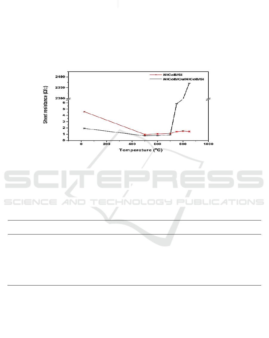
multilayer film was lower than that of monolayer film, the effect of defects on electron scattering
weakened, it may cause a lower resistance. Moreover, the Cu wafer resistance also had an effect on
the sheet resistance of the surface NiCoB film. Annealing the film from 500 °C to 700 °C, sheet
resistance of this film decreased to 0.899 / followed by an increase to 6.724 / for an annealing
up to 800 °C. However, it increased sharply after annealing at 850°C. In combination with the
results of XRD analysis, the increase of sheet resistance was due to the formation of highly resistive
Cu
4
Si. Therefore, analysis about sheet resistance suggested that the complete failure temperature of
the NiCoB barrier film in Cu interconnections is 850°C.
Figure 4. Variation of sheet resistance of NiCoB/Si and NiCoB/Cu/NiCoB/Si samples with
temperature.
Table 2 lists some electroless deposited diffusion barrier layer films of ternary system [22, 29-32].
Compared to these diffusion barrier layers, NiCoB film has a low resistivity and excellent
thermostability, so it is very promising to be applied to barrier layer.
Table 2. Electroless deposited diffusion barrier layer films and its performance [22, 29-32].
Diffusion barrier layer film
Thickness
(nm)
Resistivity
(
·cm)
Failuer temperature
(°C)
Reference
NiCoP 50 109 500 [22]
CoWP 30 80 500 [29]
NiMoP 15~20 80 700 [30]
NiMoB 40 94 500 [31]
CoMoB 30 127.5 600 [32]
NiCoB 40 18.364 850 This work
3.4. Characterization of surface morphology
Through using atomic force microscopy, surface morphologies of the electroless deposited NiCoB/Si
samples and the NiCoB/Cu/NiCoB/Si samples before and after annealing from 500 °C to 850 °C
were analyzed.
As shown in Figure 5(a) and Figure 5(b), the surface of depositedNiCoB/Si and NiCoB/Cu/,
NiCoB/Si films presented "orange peel". It can be inferred that the presence of Cu in the film stuck
affected the surface morphology.
The surface morphologies of annealed NiCoB/Cu/NiCoB/Si samples were shown from Figure
5(c) to Figure 5(h). The surface of the NiCoB/Cu/NiCoB/Si film roughened after 500°C annealing.
Research on NiCoB Diffusion Barrier Film Prepared by Electroless Deposition for ULSI-Cu Metallization
429
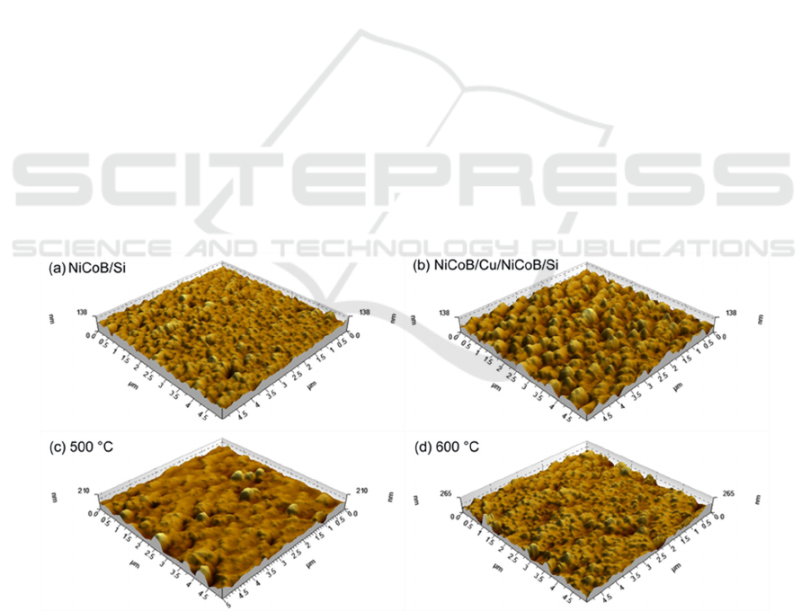
Compared with the XRD data of Figure 3, it can be concluded that the morphological change
occurred result from the development of new phases in the film, specifically Ni
3
Si
2
, B
4
Si, and CoB.
Annealing the NiCoB/Cu/NiCoB/Si film at 600°C, the overall grains were more uniform distribution
and uneven, besides, a few isolated larger grains, resulting in much larger roughness. There was an
apparent aggregation of small grains after 700 °C annealing and it was a stage that new phases were
generating in, such as Ni
3
Si, Ni
3
Si
2
and B
4
Si. After annealing at 750°C, large grains led to a larger
roughness. Some grains connected each other and appeared island-growth after 800 °C annealing,
surface became smoother and the surface energy decreased. Yet annealing at 850 °C caused the
development of small grains on the surface of the original grains. With overall consideration of XRD,
AFM and sheet resistance data, the complete failure temperature of the NiCoB barrier film in Cu
interconnections is 850°C. The failure mechanism is that after annealing at 850
C, new phases of
NiSi
2
, Ni
4
B
3
, and B
4
Si were appeared and accompanied by a large number of grain boundaries. Cu
diffused across these grain boundaries and reacted with Si-substrate. Formation of highly resistive
Cu
4
Si, causing the changes of surface morphologies and sheet resistance of NiCoB/Cu/NiCoB/Si
samples.
4. Conclusions
In this paper, NiCoB thin films were deposited by electroless deposition as single layers and as
diffusion barrier layers on Cu interconnections. XRD and XPS analyses demonstrated that the
electroless deposited NiCoB film was amorphous and it was composed of CoB compound and
elementary Ni. According to annealing experiments, it can be found that the failure temperature at
which Cu diffusion occurred was 850°C. After 850°C annealing, NiCoB barrier layer was
crystallized and grain boundaries provided channels for the diffusion of copper. Reaction between Cu
and Si-substrate resulted in the formation of Cu
4
Si which had high resistivity.
According to our study, the electroless deposited NiCoB thin film has a great promising to be
applied to diffusion barrier layer for Cu interconnections because of its excellent adhesion, low
resistivity and high failure temperature.
IWMCE 2018 - International Workshop on Materials, Chemistry and Engineering
430
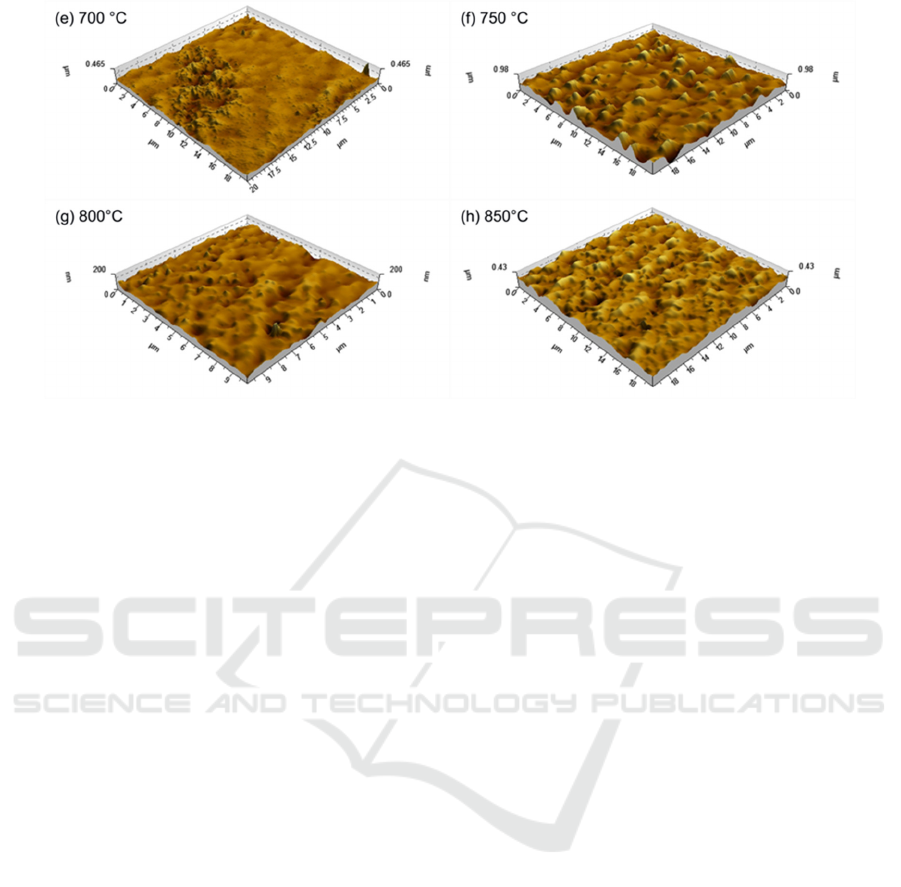
Figure 5. AFM surface morphologies of unannealed NiCoB(a) and NiCoB/Cu/NiCoB/Si (b)
samples and NiCoB/Cu/NiCoB/Si samples annealed at different temperatures((c)~(h)).
Acknowledgement
This study was supported by the National Natural Science Foundation of China (Grant No.:
51762043) and Yunnan copper based and special advanced conductive material engineering
laboratory (KC1610184).
Reference
[1] Hu C K and Harper J M E 1998 Copper interconnections and reliability Materials Chemistry
and Physics 52 5-16
[2] Murarka S P 1997 Advanced materials for future interconnections of the future need and
strategy Microelectronic Engineering 37/38 29-37
[3] Wong H Y, Mohd Shukor N F and Amin N 2007 Prospective development in diffusion barrier
layers for copper metallization in LSI Microelectronics Journal 38 777-782
[4] Yang J Y, Hong R T and Huang M J 2005 A comparative molecular dynamics study of copper
trench fill properties between Ta and Ti barrier layers Materials Science in Semiconductor
Processing 8 622-629
[5] Ofek Almog R, Sverdlov Y, Goldfarb I and Shacham-Diamand Y 2007 CoWBP capping
barrier layer for sub 90 nm Cu interconnects Microelectronic Engineering 84 2450-2454
[6] Lin L W, Liu B, Ren D, Zhan C Y, Jiao G H and Xu K W 2013 Effect of sputtering bias
voltage on the structure and properties of Zr-Ge-N diffusion barrier films Surface and
Coatings Technology 228 S237-S240
[7] Dai X H, Zhang L, Feng Z D, Li X H, Guo J X, Fu Y J, Zhou Y, Zhao Q X, Lou J Z, Ma L X,
Zhang X Y and Liu B T 2015 Barrier performance of ultrathin amorphous Nb-Ni film
between copper and silicon Materials Letters 159 94-97
[8] Lee H J, Hong T E and Kim S H 2016 Atomic layer deposited self-forming Ru-Mn diffusion
barrier for seedless Cu interconnects Journal of Alloys and Compounds 686 1025-1031
[9] Sharma S, Kumara M, Rani S, Kumar D and Tripathi C C 2016 Structural and electrical
characterization of CoNiO monolayer as copper diffusion barrier in integrated circuits
Materials Science in Semiconductor Processing 48 1–8
[10] Rha S K, Lee W J, Lee S Y, Hwang Y S, Lee Y J, Kim D I, Kim D W, Chun S S and Park C O
1998 Improved TiN film as a diffusion barrier between copper and silicon, Thin Solid
Research on NiCoB Diffusion Barrier Film Prepared by Electroless Deposition for ULSI-Cu Metallization
431

Films. 320 134-140
[11] Burgess S R, Donohue H, Buchanan K, Rimmer N and Rich P 2002 Valuation of Ta and TaN-
based Cu diffusion barriers deposited by Advanced Hi-Fill (AHF) sputtering onto blanket
wafers and high aspect ratio structures Microelectronic Engineering 64 307-313
[12] Jang S Y, Lee S M and Baik H K 1996 Tantalum and niobium as a diffusion barrier between
copper and silicon Journal of Materials Science: Materials in Electronics 7 271-278
[13] Wang W L, Peng K T, Kuo H C, Yeh M H, Chien H J and Ying T H 2014 The contact
resistance reduction of Cu interconnects by optimizing the crystal behavior of Ta/TaN
diffusion barrier Materials Science in Semiconductor Processing 27 860-864
[14] Shacham-Diamand Y, Osaka T, Okinaka Y, Sugiyama A and Dubin V 2015 30 years of
electroless plating for semiconductor and polymer micro-systems Microelectronic
Engineering 132 35-45
[15] Kohn A, Eizenberg M and Shacham-Diamand Y 2003 The role of microstructure in
nanocrystalline conformal Co0.9W0.02P0.08 diffusion barriers for copper metallization
Applied Surface Science 212-213 367-372
[16] Aithal R K, Yenamandra S, Gunasekaran R A, Coane P and Varahramyan K 2006 Electroless
copper deposition on silicon with titanium seed layer, Materials Chemistry and Physics 98
95-102
[17] Hamid Z A, Aal A A, Shaaban A and Hassan H B 2009 Electrodeposition of CoMoP thin film
as diffusion barrier layer for ULSI applications Surface and Coatings Technology 203
3692-3700
[18] Tarozait R, Sukackien Z, Sudaviius A, Jušknas R, Selskis A, Jagminien A and Norkus E
2009 Application of glycine containing solutions for electroless deposition of Co-P and Co-
W-P films and their behavior as barrier layers Materials Chemistry and Physics 117 117–
124
[19] Chen S T, Liu Y Y and Chen G S 2015 Ultrathin cobalt-alloyed barrier layers for copper
metallization by a new seeding and electroless-deposition process Applied Surface Science
354 144-147
[20] Einati H, Bogush V, Sverdlov Y, Rosenberg Y and Diamand Y S 2005 The effect of tungsten
and boron on the Cu barrier and oxidation properties of thin electroless cobalt-tungsten-
boron films Microelectronic Engineering 82 623-628
[21] Dulal S M S I, Kim T H, Rhee H, Sung J Y and Kim C K 2009 Development of an alkali-
metal-free bath for electroless deposition of Co-W-P capping layers for copper
interconnections Journal of Alloys and Compounds 467 370-375
[22] Kumar A, Kumar M K and Kumar D 2012 Effect of composition on electroless deposited Ni-
Co-P alloy thin films as a diffusion barrier for copper metallization Applied Surface Science
258 7962-7967
[23] Sudagar J, Lian J S and Sha W 2013 Electroless nickel, alloy, composite and nano coatings-A
critical review Journal of Alloys and Compounds 571 183-204
[24] Saito T, Sato E, Matsuoka M and Iwakura C 1998 Electroless deposition of Ni-B, Co-B and
Ni-Co-B alloys using dimethylamineborane as a reducing agent Journal of Applied
Electrochemistry 28 559-563
[25] Wang S L 2007 Electroless deposition of Ni-Co-B alloy films and influence of heat treatment
on the structure and the magnetic performances of the film Thin Solid Films 515 8419-8423
[26] Narayanan T S N S, Stephan A and Guruskanthan S 2004 Electroless Ni-Co-B ternary alloy
deposits: preparation and characteristics Surface and Coatings Technology 179 56-62
[27] Gamboa S A, Gonzalez-Rodriguez J G, Valenzuela E, Campillo B, Sebastian P J and Reyes-
Rojas A 2006 Evaluation of the corrosion resistance of Ni-Co-B coatings in simulated
PEMFC environment Electrochimica Acta 51 4045-4051
IWMCE 2018 - International Workshop on Materials, Chemistry and Engineering
432

[28] Wang H M, Yu Z B, Chen H Y, Yang J and Deng J F 1995 High activity ultrafine Ni-Co-B
amorphous alloy powder for the hydrogenation of benzene Applied Catalysis A: General
129 L143-L149
[29] Kohn A, Eizenberg M, Shacham-Diamand Y, Israel B and Sverdlov Y 2001 Evaluation of
electroless deposited Co (W,P) thin films as diffusion barriers for copper metallization
Microelectronic Engineering 55 297-303
[30] Chou Y H, Sung Y, Liu Y M, Pu N W and Ger M D 2009 Amorphous Ni-Mo-P diffusion
barrier deposited by non-isothermal deposition Surface and Coatings Technology 203
1020-1026
[31] Wang Y C, Chen X H, Ma W H, Liu X M, Li Y P, Bi P and Xiang F W 2017 Electroless
Deposition of NiMoB Diffusion Barrier Layer Film for ULSI-Cu Metallization Key
Engineering Materials 727 900-906
[32] Liu X M, Chen X H, Ma W H, Li Y P, Bi P, Wang Y C and Xiang F W 2016 Electroless
CoMoB Diffusion Barrier Layer for ULSI-Cu Metallization Materials Science Forum 847
91-96
Research on NiCoB Diffusion Barrier Film Prepared by Electroless Deposition for ULSI-Cu Metallization
433
