
A 0.13 μm BiCMOS Reconfigurable Analog Baseband for
Multi-mode Multi-standard Wireless Receivers
Jian Tao and Xiangning Fan
Institute of RF-&OE-ICs, School of Information Science and Engineering, Southeast University, Nanjing, China
Keywords: Analog Baseband (ABB), Reconfigurable, Multi-mode Multi-standard, BiCMOS.
Abstract: This paper presents a reconfigurable analog baseband (ABB) for multi-mode multi-standard wireless
applications. By having digitally controllable transconductance and transimpedance amplifier stages, the
gain, noise figure (NF) and linearity of the analog baseband can be reconfigured. Fabricated in IBM 0.13
μm BiCMOS process, the analog baseband achieves voltage gain from 4.4 to 33.3 dB. Simulated maximum
input 1-dB compression point and input intercept point (IIP3) are 1.2 dBm and 11.2 dBm respectively.
Simulated minimum noise figure is 9.4 dB. The current consumption for a single branch (I or Q) ranges
from 3.5 to 4.5 mA from 1.8 V supply voltage. The chip occupies an area of 0.2 mm
2
.
1 INTRODUCTION
Recently, various kinds of wireless applications for
handset mobile terminals are emerging and
industries are making great effort to enable mobile
terminals to support all functionalities related to
various existing and new born communication
standards. It is hoped that, those mobile terminals,
with low price and low power consumption, can
provide us high-quality services including long
distance communications (e.g., TD/FD-LTE,
WCDMA, GSM, Satellites) and short range
communications (e.g., WLAN, WPAN, UWB) (Lin
et al., 2015). It is necessary to design a receiver,
which is compatible with multiple communication
standards.
Software defined radio (SDR), which is
innovated to use digital receiving and transmitting
instead for analog processing of signals (Abidi,
2007), provide us a new way to realize the
integration of different function in one terminal.
However, SDR put so stringent requirement on
analog to digital converters (ADC) that it can hardly
be realized nowadays. An evolved SDR architecture
can be used to organize a receiver, which is
essentially a reconfigurable zero intermediate
frequency receiver as shown in Fig. 1. This receiver
can be tuned to any carrier frequency, with any
signal bandwidth, any modulation fashion. The
flexible reconfigurability requires that every
circuitry block of the receiver should be
reconfigurable.
Figure 1: The block diagram of the reconfigurable
receiver.
One of the key building blocks for multi-mode
multi-standard receiver is the analog baseband (ABB)
circuit, which consists of a transconductor stage and
a transimpedance (TIA) stage. The gain of the ABB
should be reconfigurable to provide several degrees
of freedom. Some ABBs have been proposed (Kwon
and Han, 2014; Hedayati et al., 2015), however, the
gain cannot be tuned and the receiver could be
blocked by interference signals. In this paper, we
present an ABB with a bias circuit. The ABB can be
flexibly reconfigurable in terms of gain, which is a
great advantage for multi-mode multi-standard
receiver.
The paper is organized as follows: The
reconfiguration arrangement and design
considerations for ABB are presented in Section 2
and 3. Simulated results are shown in Section 4.
Finally, conclusions are drawn in Section 5.
100
Tao, J. and Fan, X.
A 0.13 µm BiCMOS Reconfigurable Analog Baseband for Multi-mode Multi-standard Wireless Receivers.
DOI: 10.5220/0006414501000104
In Proceedings of the 7th International Joint Conference on Pervasive and Embedded Computing and Communication Systems (PECCS 2017), pages 100-104
ISBN: 978-989-758-266-0
Copyright © 2017 by SCITEPRESS – Science and Technology Publications, Lda. All rights reserved
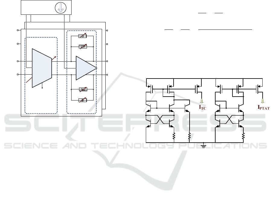
2 RECONFIGURATION
ARRANGEMENT
The block diagram of the reconfigurable ABB is
illustrated in Fig. 2. The proposed ABB includes
symmetrical I/Q branches and bias cell. Each of I
and Q branches is composed of a reconfigurable
transconductor stage and a reconfigurable TIA stage.
Figure 2: The block diagram of the reconfigurable ABB.
This ABB is similar to a standard linear current
mode receiver based on a low-noise
transconductance amplifier (LNTA) + mixer + TIA.
As no mixer is needed, the noise requirement is
relaxed thanks to the preceding low-noise amplifier
(LNA) gain (Borremans et al., 2011). The voltage
gain of the ABB is derived as:
A
G
vc
R
vc
(1)
where
is the transconductance of the
transconductor stage,
is the transimpedance of
the TIA stage. The value of
and
is
controlled by the 2-bit control word (
,
),
therefore the ABB has 4 gain modes. Along with the
reconfiguration of gain, the noise figure (NF),
linearity and power consumption of the ABB can be
reconfigurable according to the different
communication standards.
3 DETAILED CIRCUIT DESIGN
In this section, the circuit design of the analog
baseband shown in Fig.2 is presented in detail.
3.1 Bias Circuit
A better performance can be obtained by using a
constant transconductance bias circuit. As shown in
Fig. 3, the whole circuit DC bias points are provided
by a proportion to absolute temperature (PTAT) bias
network for BJT and a temperature compensation
(TC) bias network for MOS to ensure constant
transconductance. The bias current are given (Razavi,
2001):
I
ln
(2)
I
2V
R
ln
A
A
.
V
,
V
,
V
,
R
.
(3)
where
is the thermal voltage, A is the emitter area
of bipolar transistor, and
is the base-emitter
voltage of bipolar transistor.
Figure 3: The bias circuit for the ABB.
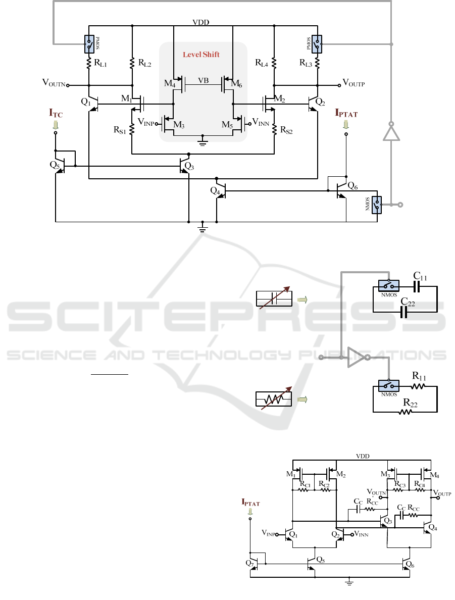
3.2 Transconductor Stage
The schematic of the reconfigurable transconductor
stage is illustrated in Fig. 4. The input DC voltage is
very low (e.g., 0.3V) for reducing the on-resistance
of the mixer, so the level shift circuit is necessary to
offer an appropriate DC point. The transconductor
stage is the combination of a fixed transconductor
and a
-controlled transconductor. The fixed
transconductor are provided by MOS transistors M
1
and M
2
. The source negative feedback resistors R
S
can further increase linearity. The other parallel
branch is consisted by BJT Q
1
and Q
2
, which can
offer a lager transconductance. NMOS switch is
used to control on and off of the BJT branch, PMOS
switches are used to maintain the output operating
point stable.
3.3 TIA Stage
TIA works as a current amplifier and converts
V
IN-I
2
()
TIA
Cvc
2
()
TIA
R
vc
2
()
TIA
R
vc
2
()
TIA
Cvc
V
IN-Q
V
OUT-Q
V
OUT-I
1
vc
G
m
OTA
In-Phase
Quadrature-Phase
Bias Cell
TIA stage
G
m
stage
2
R
1
Q
DD
V
2
Q
3
Q
4
Q
5
Q
1
R
3
R
6
Q
7
Q
8
Q
9
Q
1
M
2
M
3
M
4
M
5
M
6
M
A 0.13 µm BiCMOS Reconfigurable Analog Baseband for Multi-mode Multi-standard Wireless Receivers
101
1
vc
Figure 4: Circuit of the transconductor stage.
current signal to voltage signal at output. The TIA
also provides some low-pass characteristic for
channel selection and interference attenuation. The
transimpedance is determined by the feedback
resistor R
. The reconfigurable gain is realized by
the paralleling the resistors, as shown in Fig. 5.
The cut-off frequency is depended on the R
and the feedback capacitor C
:
ω
1
R
C
(4)
and
are controlled by two opposite control
words to make their product is unchanged. So the
bandwidth does not change with various gains.
The operational transconductance amplifier
(OTA) with a high gain-bandwidth (GBW) is
necessary to reduce the input impedance of the TIA
which can be close to zero in a wideband. This paper
adopts a 2-stage miller-compensated OTA (Willy,
2006) which is depicted in Fig. 6. This fully-
differential amplifier uses four equal resistors
(R
R
) to cancel out the differential signals and
offer the common-mode biasing voltage.
2
()
TIA
R
vc
2
()
TIA
Cvc
2
vc
Figure 5: Realization of the reconfigurable C
and R
.
Figure 6: Circuit of OTA in the TIA stage.
SPCS 2017 - International Conference on Signal Processing and Communication Systems
102
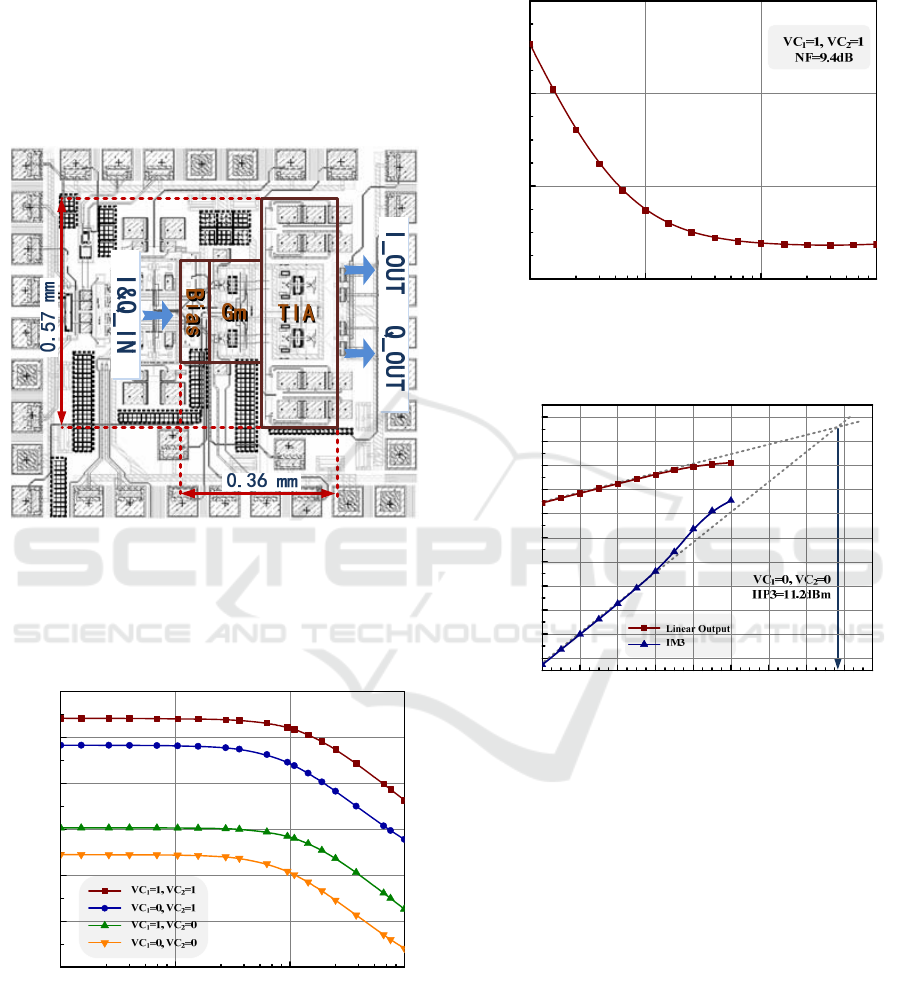
4 LAYOUT AND
POST-SIMULATED RESULTS
The layout of the whole ABB by using IBM 0.13μm
BiCMOS process is shown in Fig. 7. The overall
area is 0.57μm 0.36μm. The supply voltage of the
chip is 1.8V and the power consumption is 14.2/17.8
mW (without output buffer).
Figure 7: Layout of the baseband circuit.
Fig. 8 illustrates the post-simulated of voltage
gain curves with various
and different size of
. 4 gain steps (34.3/28.3/10.4/4.4 dB) are clearly
shown to meet different applications.
0.1 1 10 100
-20
-10
0
10
20
30
40
Voltage Gain (dB)
Frequency (MHz)
Figure 8: Post-simulated of gain curves with different G
and R
.
The ABB has the minimum NF of 9.4 dB at the
highest gain mode as shown in Fig. 9. And it has
best linearity under the lowest gain mode. The
highest post-simulated IIP3 is about 11.2 dBm with
two-tone signals
1.06MHz and
1MHz
as shown in Fig. 10.
10
5
10
6
10
7
10
8
8
12
16
20
Noise Figure (dB)
Fre
q
uenc
y
(
Hz
)
Figure 9: Post-simulated of NF under the highest gain
mode.
-20 -16 -12 -8 -4 0 4 8 12
-80
-70
-60
-50
-40
-30
-20
-10
0
10
20
Output Power (dBm)
Frequency (MHz)
Figure 10: Post-simulated of IIP3 under the lowest gain
mode.
Tables 1 summarize the measured results of the
proposed reconfigurable baseband circuit and give a
comparison with other recently published works.
The comparison indicates that the proposed analog
baseband exhibits wide-controllable gain range, low
noise figure and good linearity performance.
5 CONCLUSION
This paper presents a reconfigurable analog
baseband (ABB) circuit for multi-mode multi-
standard applications. The reconfiguration
arrangement and block design considerations are
described. The design concept is verified by
implementing in IBM 0.13μm BiCMOS process.
A 0.13 µm BiCMOS Reconfigurable Analog Baseband for Multi-mode Multi-standard Wireless Receivers
103

Table 1: Performance comparison.
This Work
ASICON
(Jiachen, Zheng, and
Baoyong, 2015)
J.Semicond.
(Fan, Tao, Bao, and
Wang, 2016)
TMTT
(Namsoo, Vladimir,
and Lawrence, 2010)
Technology 0.13μm BiCMOS 65n
m
CMOS 0.18 μm CMOS 0.18 μm CMOS
Gain (dB) 4.4~33.3 0
~
58 4~22 22.5~25
Bandwidth (MHz) 10 4 12 NA
Min Noise Figure (dB) 9.4 30.7 9 8
IIP3 (dBm) 11.2 -27(@58dB) 9 7
Supply Voltage (V) 1.8 1.2 1.8 2
Bias curren
t
(mA) 3.5~4.5 1.9
~
2.1 8.2~13.2 5
Note Gm+TIA Gm+TIA
Gm+mixer
+TIA
Gm+mixer
+TIA
The ABB can achieve 4 gain steps, high linearity
and low noise performance at the desired gain mode.
The proposed ABB provides a good alternative in
the applications of multi-mode multi-standard
wireless communications.
ACKNOWLEDGEMENTS
This paper is supported by the National Basic
Research Program and the Priority Academic
Program Development of Jiangsu Higher Education
Institutions. And we are grateful for the encouraging
discussions and technique assistances of the whole
team in Institute of RF- & OE-ICs, Southeast
University.
REFERENCES
Lin, F., Mak, p., and Martins, R. P., 2015. Wideband
Receivers: Design Challenges, Tradeoffs and State-of-
the-Art, Circuits and Systems Magazine, vol.13, no.1,
pp.12-24.
Abidi, A., 2007. The path to SDR receiver, IEEE Journal
of Solid-State Circuits, vol.42, no.5, pp.954-966.
Kwon, K., and Han, J., 2014. A 2G/3G/4G SAW-Less
Receiver Front-End Adopting Switchable Front-End
Architecture, IEEE Trans Microwave Theory Tech.,
vol.62, no. 8, pp. 1097-1111.
Hedayati, H., Lau, W., A., Kim, N., Aparin, V., and
Entesari, K., 2015. A 1.8 dB NF Blocker-Filtering
Noise-Canceling Wideband Receiver with Shared TIA
in 40 nm CMOS, IEEE Journal of Solid-State
Circuits, vol.50, no.5, pp. 1148-1164.
Borremans, J., Mandal, G., Giannini, V., Debaillie, B.,
Ingels, M., Sano, T., Verbruggen, B., and Craninckx,
J., 2011. A 40 nm CMOS 0.4–6 GHz Receiver
Resilient to Out-of-Band Blockers, IEEE Journal of
Solid-State Circuits, vol.46, no.7, pp.1148-1164.
Razavi, B., 2001. Design of Analog CMOS and Integrated
Circuits, McGraw Hill. United States, 2
nd
edition.
Willy, M.C., 2006. Analog Design Essentials, Springer.
United States, 1
st
edition.
Jiachen, H., Zheng S., and Baoyong C., 2015. A
reconfigurable analog baseband for low-power Wi-Fi
receiver, IEEE 11th International Conference on ASIC
(ASICON), pp.1-4.
Fan, X., Tao, J., Bao, K., and Wang, Z., 2016. A
reconfigurable passive mixer for multimode
multistandard receivers in 0.18 m CMOS, Journal of
Semiconductors, vol.37, no.8, pp.085001-1-8.
Namsoo, K., Vladimir, A., and Lawrence, L., 2010. A
resistively degenerated wideband CMOS passive
mixer with low noise figure and high IIP2, IEEE
Trans. Microwave Theory Tech., vol.58, no.4,pp.820-
830.
SPCS 2017 - International Conference on Signal Processing and Communication Systems
104
