
Decorrelation of the Light-emitting-Diode
Internal-quantum-Efficiency Components
Studies of the Electron-hole Concentration-ratio at the Active-region Edge
Dinh Chuong Nguyen
1,2
, David Vaufrey
1,2
and Mathieu Leroux
3
1
Univ. Grenoble Alpes, F-38000, Grenoble, France
2
CEA, LETI, MINATEC Campus, F-38054, Grenoble, France
3
CNRS – Centre de recherche sur l’Hétéro-Epitaxie et ses Applications (CRHEA),
Rue Bernard Grégory, 06560, Valbonne, France
1 RESEARCH PROBLEM
GaN-based light-emitting diodes (LEDs) have
strongly emerged, especially since the last decade, as
a very promising white-light source, enabling them
to enter many lighting applications and even further.
Those applications mostly required the LEDs to
function at a high-current regime. However, LEDs
still suffer a critical internal-quantum-efficiency
(IQE) loss, known as “droop”. Their IQE falls
drastically at high current-injection after reaching a
peak value at usually relatively low current-densities
(Krames et al., 2007; Morkoç, 2008), degrading the
radiative-recombination rate and the output power
(Cabalu et al., 2006; M.-H. Kim et al., 2007), a
behavior that can be described as a sublinear
increase in light-emission intensity with increasing
diode current-density. The efficiency droop was first
observed in GaN-based LEDs by (Krames et al.,
2000) and (Mukai et al., 1999). The loss’ main
mechanism still remains an important topic that has
raised intense debate by many reasons.
First, the knowledge about the wurtzite GaN is
not complete as several parameters still suffer from
uncertainty, such as the recombination coefficients
or the carrier mobility. The Auger-recombination
coefficients obtained from numerical calculations
and curve-fitting can largely differ from each other,
even though it is related to one of the widely-
accepted droop-inducing processes. The carrier-
mobility variation in GaN is noticed to be different
from that in the well-understood Si, yet only one
model for electron mobility was proposed (Turin,
2005).
Second, though theoretically explained, the
internal mechanisms, especially the recombination,
cannot be separately evaluated by characterization,
or at least in an easy way. Their discrimination is
critical as they can replace each other as the main
loss-inducing mechanism in respect to the LED
functioning-regimes. It has been attempted several
times but the results are still under discussion.
The aforementioned difficulties hinder the droop
reducing but the research activities are still ongoing.
However, in addition to the applied methods, it may
be suggested that new approaches be proposed.
2 OUTLINE OF OBJECTIVES
The LED efficiency-loss being complicated and
involving many different mechanisms that cannot be
easily and separately studied, this PhD. thesis thus
aims to contribute to the decorrelation of these
different droop-inducing factors. It mainly focuses
on the ratio between the electron and hole
concentrations that are injected into the active region
of an LED and contribute to light emission.
Nonetheless, other non-radiative recombination
processes are also taken into account.
This work consists in two parts: LED modeling
and characterizing. The samples are mostly
commercial LEDs but can also be provided by
internal research-projects. Initially, the modeling is
expected to provide an insight into the LED internal-
mechanisms in order to evaluate the impact of each
mechanism on the efficiency loss. The
understanding of those impacts’ degree could help
design a more innovative LED structure in which the
mechanisms favorable to the LED lighting-function
are intensified and the loss-inducing ones are
reduced. The characterization allows to verify the
hypothesis deduced from the simulation.
However, a simulation can also be carried out
based on characterization results since the efficiency
on several internal-project-LEDs can show a strong
improvement without its reasons being clearly
explained.
37
Nguyen D., Vaufrey D. and Leroux M..
Decorrelation of the Light-emitting-Diode Internal-quantum-Efficiency Components - Studies of the Electron-hole Concentration-ratio at the Active-region
Edge.
Copyright
c
2015 SCITEPRESS (Science and Technology Publications, Lda.)

Based on the acquired knowledge from modeling
and characterization, as stated above, more-
innovative high-power LED structures are expected
to be designed.
3 STATE OF THE ART
Many groups have proposed different mechanisms
that they judge to be the main reason of the LED
droop. Those mechanisms are very diverse but as
until 2014, two mainstream processes remain most
relevant to the IQE droop.
On the one hand, (Hader et al., 2008) have
simulated the magnitude of direct Auger-
recombination in the (AlGaIn)N material system and
concluded that Auger losses are too small to account
for the droop. Meanwhile, by taking phonon-assisted
Auger-recombination into account, (Kioupakis et al.,
2011) were able to obtain higher Auger-coefficient
values which are in good agreement with the
experiments (Galler et al., 2012). (Delaney et al.,
2009) have computed the Auger coefficient by the
first-principles density-functional and reported
values that can be as large as 2 × 10
–30
cm
6
s
–1
when
the bandgap is approximately 2.5 eV, enabling the
Auger processes to be the main cause of the droop.
However, this coefficient is significantly reduced as
the band gap is higher or lower than 2.5 eV. (Iveland
et al., 2013) have gone further by directly measuring
the Auger-induced electrons from an LED under
electrical injection and concluded that the Auger
processes are the origin of the droop phenomenon.
Comments upon their results were given by
(Bertazzi et al., 2013).
On the other hand, by comparing the optical and
electrical properties of AlGaInN-barrier-enhanced
LEDs with those of GaN-barrier-enhanced LEDs,
(Schubert et al., 2008) suggested that carrier leakage
might be the dominant cause of the efficiency droop.
Through experiments and simulation of the
polarization-field-enhanced carrier-leakage, (M.-H.
Kim et al., 2007) also strengthened this assumption.
Other works based on electron leakage enhanced by
high internal piezoelectric fields were published
elsewhere (Rozhansky and Zakheim, 2007; Schubert
et al., 2007; Xu et al., 2009). It was also suggested
that poor hole-injection may reduce the efficiency
(David et al., 2008; Ni et al., 2008; Zhang et al.,
2014).
Apart from these two main schools of thought,
several groups have indicated other different
mechanisms that may lead to the LED efficiency-
droop, including recombination at dislocation
(Hangleiter et al., 2005), self-heating as the current
increases (Cao and Arthur, 2004). Recently, (Huang
et al., 2013) reported the effect of the lateral current-
spreading on the efficiency droop in a conventional-
chip LED. Studies on current spreading in vertical
LEDs were also carried out (Li and Wu, 2012; Son
et al., 2012). In this paper, the mentioned samples
and simulation models are both vertical-thin-film
(VTF) LEDs. A VTF LED structure is flipped from
the conventional epitaxial stack, with an n-type layer
under a p-type layer and the cathode facing the
anode. The experimental results and the
corresponding simulations will be reported and show
that the efficiency droop in VTF GaN-based LEDs is
partly tuned by spreading.
4 METHODOLOGY
As the semiconductor-device simulation is mainly
numerical, the initial approach is to build a model
for GaN-based LEDs by analytically solving the
mathematical expressions. These expressions are
interconnected and solving them involves the use of
special functions; hence analytical solutions can
hardly be obtained.
Another approach was then carried out. Since the
current passing through an LED mainly consists in
electrons due to their low effective-mass and high
mobility, while the amount of emitted-light is tuned
by the holes as they are minority carriers, the
electroluminescence characterization can provide an
estimation of the ratio between these carriers.
Furthermore, through pulsed-electroluminescence
characterizations, their injection efficiencies can be
evaluated due to the difference in mobility.
Consequently, a pulsed-electroluminescence setup
was realized. The recorded data were later processed
and compared to the simulation results in a
following communication.
As for the modeling, the ATLAS package from
SILVACO Corporation is utilized. The carrier
concentration is calculated with special attention,
especially at the edges of the active region, because
their enhancing or limiting role will become clear at
these positions. The simulation can be coupled with
characterization whether to verify the modeling
accuracy or to explain the measurements. The work
presented later in this paper was based on the
characterization results from two different LED-
structures. The simulation was later carried out to
partly explain the observed changes between the two
structures. Deeper studies on the carrier
concentrations followed and provided an insight into
PHOTOPTICS2015-DoctoralConsortium
38

the unbalanced distributions of electrons and holes
entering the active region, where they might
eventually recombine. This observation then
suggested that the p-type layer play an important
role in the carrier transport and lead to the p-GaN-
properties studies through characterization.
5 EXPECTED OUTCOME
The electroluminescence measurements show a time
shift between the onset of the current signal and that
of the luminous signal. This shift is expected to
represent the different degrees of carrier-injection
efficiency if it varies with regard to the material
parameters. The data processing was still ongoing
when this article was being written.
The studies on the p-GaN properties could
provide additional information needed to better
understand the carrier behaviors and their impact on
the efficiency loss. They can help complete the
modeling and eventually establish the ratio between
the electron and the hole concentrations, hence this
ratio’s weight in the IQE droop can hopefully be
estimated. Sample preparations are expected to be
finished shortly.
If these goals are achieved, by the end of this
PhD. thesis, new ideas for a more efficient LED-
design might be proposed.
6 STAGE OF THE RESEARCH
In this paper, the work carried out through modeling
will be presented. Its results will be applied in the
incoming works.
This work started from the characterization
results obtained on a project’s samples, followed by
the ATLAS software package simulation.
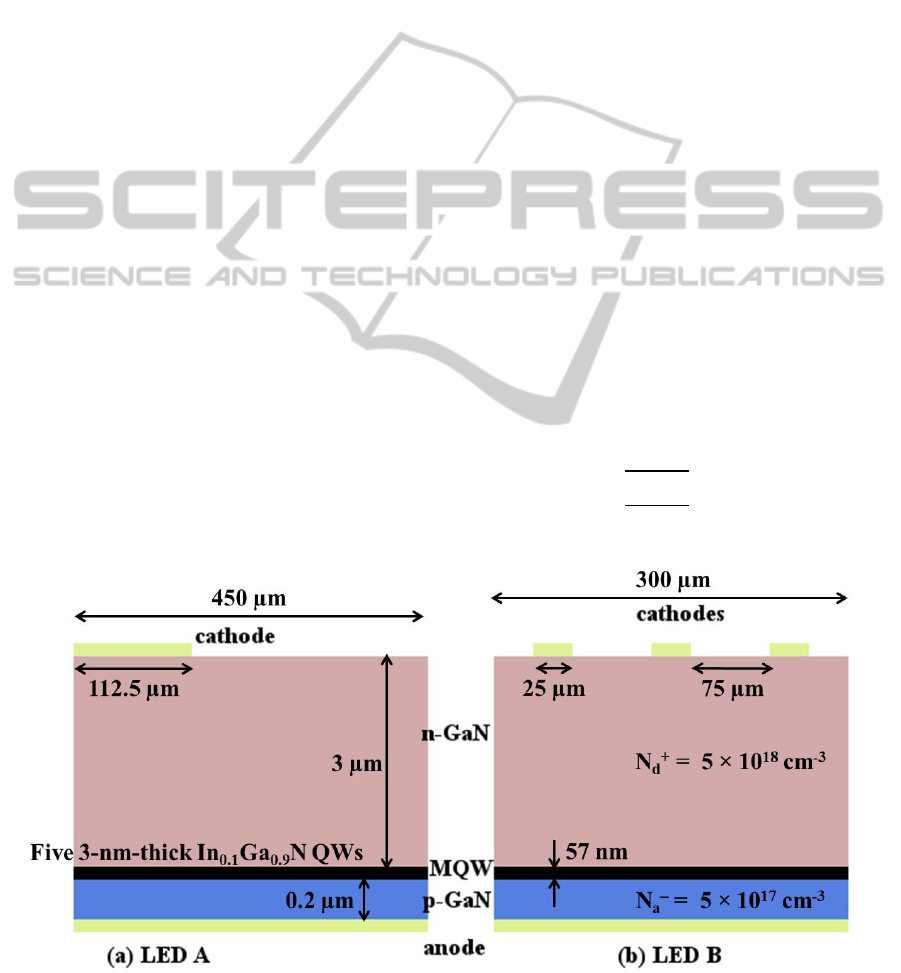
6.1 Sample Structure and Simulation
Model
Two sample structures were fabricated, electrically
and optically characterized. Those are square
900 µm × 900 µm LEDs, differing from each other
only in their cathode. The first structure, hereby
called LED 1, has a round 100-µm-diameter
cathode, situated in the middle of its surface. The
second structure, LED 2, has multiple-stripe-like
cathodes that are parallel to each other. These two
structures were modeled as described below with the
same parameters. Though the structure used to
model the LED 1 does not possess a round cathode,
its section should resemble that of the LED 1.
To simulate the aforementioned LED 1 and
LED 2, two vertical GaN-based LED structures with
different-shaped cathodes are modeled: the LED A
has a single-striped cathode that is placed in the
middle of the p-type surface, while the LED B has
nine striped-cathodes that are parallel to each other.
Their widths are also 900 µm. In the LED A, the
cathode width is set to 225 µm. The cathodes in the
LED B are 25 µm-wide and separated from each
other at a distance of 75 µm. Consequently, in both
structures, the total area covered by the cathodes is
equivalent. The p-type layer is 3-µm-thick and the
ionized-acceptor concentration is 5 × 10
17
cm
–3
. The
n-type-layer thickness and ionized-donor
concentration are respectively kept at 3 µm and
5 × 10
18
cm
–3
. All the doping profiles are uniform.
Both structures also consist of five 3-nm-thick
undoped In
0.1
Ga
0.9
N quantum wells, separated by
four 10-nm-thick GaN barriers. However, neither of
them consists of an electron-blocking layer (EBL).
The anode covers the full surface of the LED
structures. Both the anode and cathode are
considered to be ohmic contacts. The section of one-
half of the LED A is shown in Figure 1(a) and the
section of one-third of the LED B is shown in Figure
1(b). Note that they are not in exact scale.
As stated before, the simulations were carried out
on the ATLAS software package by SILVACO
Corporation. Standard Shockley-Read-Hall (SRH),
Auger and three-band radiative-recombination
models are used to respectively simulate the non-
radiative and radiative mechanisms. For the SRH
model, the electron and hole lifetimes are both fixed
at 100 ns. This value is high compared to those
reported in the state of the art but approximate to
those reported by (Delaney et al., 2009) and will
reduce the SRH-recombination rate. Meanwhile, the
trap energy level for this recombination is situated in
the middle of the band gap, meaning that the highest
possible SRH-recombination rate is computed. The
electron and hole Auger-coefficients are set to be
10
–30
cm
6
s
–1
, a larger value than the usually reported
ones in the state of the art in order to enhance Auger
recombination. The built-in electric charges
occurring at the p-n interface due to spontaneous and
piezoelectric polarization were also calculated. Its
theoretical value is usually reduced due to screening
effects, but the extent of this reduction is still
uncertain (Della Sala et al., 1999; Piprek et al., 2006;
Romanowski et al., 2010). Hence, in our simulation,
the final polarization charge density is assumed to be
80% of the theoretical value. The defect-related loss
DecorrelationoftheLight-emitting-DiodeInternal-quantum-EfficiencyComponents-StudiesoftheElectron-hole
Concentration-ratioattheActive-regionEdge
39
was not taken into account during the simulation and
the temperature is kept at 300 K.
Several other assumptions were made to simplify
the simulations. The electron and hole mobility are
respectively 400 cm
2
/Vs and 8 cm
2
/Vs. However, in
the InGaN quantum wells, they are both 100 cm
2
/Vs.
All these values are suggested by ATLAS. They are
kept constant throughout the simulation for two
main reasons. The first one is to lighten the model.
The second one is the lack of empirical models for
electron and hole mobility, especially under the
effect of a high electric field, except the model
proposed by (Turin, 2005). That being said, at high
injection currents, the modeled LED-behaviors will
deviate from the common experimental
characteristics.
In order to simulate the light output, the
radiative-recombination rate is only integrated over
the areas that are not shaded by the cathodes.
6.2 Experimental Results
The experimental results obtained on a set of
samples are plotted in Figure 2. It can be clearly
seen in Figure 2(a) that the IQE and especially its
peak-value are higher in the LED 2 than in the
LED 1. Moreover the current density corresponding
to this peak value is also higher in the LED 2 than in
the LED 1, shifted to approximatively 15 A/cm
2
instead of 10 A/cm
2
.
Furthermore, Figure 2(b) displays the normalized
IQE from the two LEDs. The droop is more
significant in the LED 1 than in the LED 2, with
efficiency falling to less than 40 % of the peak value
at 100 A/cm
2
. The forward-current density and the
optical-power density of the LED 2 also respectively
exceed those of the LED 1, as shown on Figure 2(c)
and Figure 2(d). These results imply that by
replacing a round cathode by a multiple-arrayed
cathode, the LED performance can be critically
enhanced and the droop reduced. To further
understand this difference, the next sections will
discuss the simulation results for the LEDs A and B
which are representative for the LEDs 1 and 2,
respectively.
6.3 Studies by Modeling
6.3.1 Current-spreading Analysis
Due to the multiple-stripe-like cathode-geometry,
current spreading certainly occurs in the LED
structure. The current spreading length was shown to
depend on the forward voltage and for GaN-based
LEDs, the Thompson spreading-current model was
demonstrated to be more appropriate than the Guo-
Schubert model (H. Kim et al., 2007). Since the
stripe-like electrodes in our experiments are located
on a thick n-type layer, the current is more likely to
totally spread throughout the n-type layer before
entering the p-type layer. Thus, the current-
spreading is mainly considered to occur in the n-
layer and its length was calculated for the two LEDs
A and B by the Thompson model (Thompson, 1980)
(1)
Figure 1: (a) One-half of the LED A; (b) One-third of the LED B with three cathodes. The material parameters are the same
in both structures; hence they are displayed in only one of the structures.
PHOTOPTICS2015-DoctoralConsortium
40
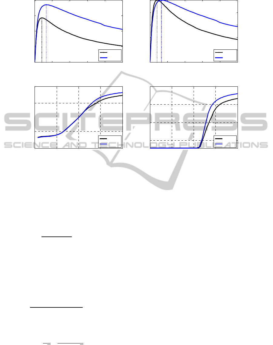
Figure 2: The experimental results from the LED 1 (black solid line) and the LED 2 (blue solid line), respectively a)
Efficiency, b) Normalized efficiency, c) J-V characteristic curve and d) L-V curve.
where n, k
B
, T, t
n
, q, ρ
n
are respectively the ideality
factor, the Boltzmann constant, the temperature, the
n-layer thickness, the elementary charge and the n-
layer resistivity. J
0
is the current density at the edge
of the contact. The current density J(x) extending
away from the contact is given by
2
/
2
(2)
J
0
can be approximated as the uniform current-
density under the cathodes, which can be measured
from the simulation. The n-type layer resistivity was
approximated by
and the ideality
factor was extracted from the simulated J-V curve as
/
/
. Included in the
equation Error! Reference source not found., this
gives
/
(3)
An integral of the equation (2) from the edge of the
contact to a position t gives
2
1
√
2
1
/
√
2
(4)
which represents the electric-current intensity per
unit length covering from the contact edge to the
position t. By multiplying it by the number of the
unshaded areas in the LEDs A and B, one obtains
the current intensity per unit length in the whole part
of the LED where light extraction is not hindered by
the opaque cathodes. The formula (4) also suggests
that a higher current-injection is more likely
achieved when the distance t is lower than L
s
.
The calculations indeed indicate that the LED B
with the multiple-striped cathodes injects a higher
current intensity than the LED A with the single-
striped cathode. However, this information still
cannot fully explain the shift of the IQE peak and
the IQE increase. As shown by Figure 3, the IQE of
the LED B at a certain current density can remain
higher than that of the LED A at a lower current
density while intuitively the IQE should decrease as
the current density increases. An insight into the IQE
is then needed and presented in the next section.
6.3.2 Internal-quantum-Efficiency and
Carrier-concentration Profile
Figure 3 shows the calculated internal quantum
efficiency (IQE) from the two LEDs. It can be seen
that the highest IQE value from the LED B is larger
than that of the LED A, reaching nearly 70 %. The
current density corresponding to this peak value is
approximately 6 A/cm
2
, also exceeding that of the
0 20 40 60 80 100
0
0.2
0.4
0.6
0.8
Current Density (A/cm
2
)
IQE (Arbitrary Unit)
(a) IQE
LED 1
LED 2
0 1 2 3 4
10
-5
10
0
(c) J-V
Voltage (V)
Current Density (A/cm
2
)
LED 1
LED 2
0 20 40 60 80 100
0
0.2
0.4
0.6
0.8
1
Current Density (A/cm
2
)
Normalized IQE
(b) Normalized IQE
LED 1
LED 2
0 1 2 3 4
10
-4
10
-2
10
0
10
2
(d) Optical Power Density
Voltage (V)
Optical Power Density (W/cm
2
)
LED 1
LED 2
DecorrelationoftheLight-emitting-DiodeInternal-quantum-EfficiencyComponents-StudiesoftheElectron-hole
Concentration-ratioattheActive-regionEdge
41
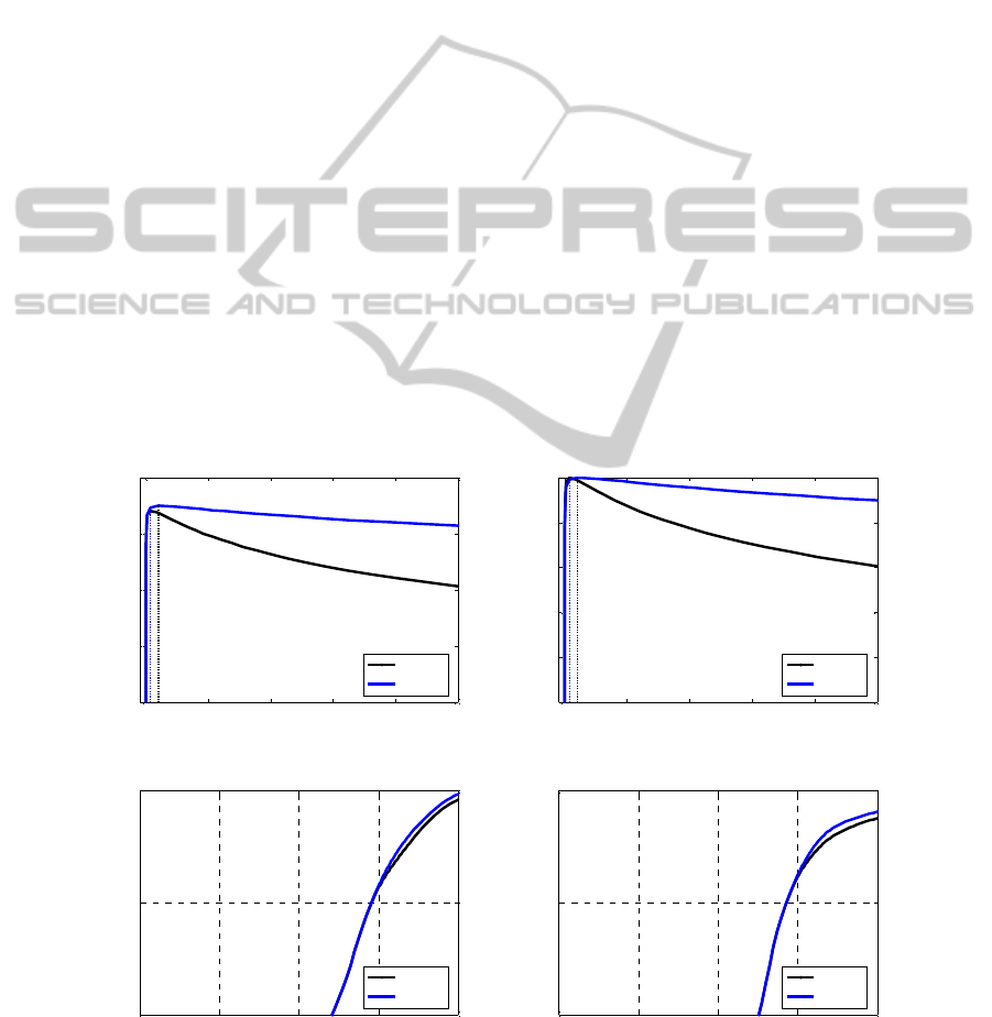
LED A. Moreover, after reaching their peak values,
while the IQE of the LED A is drastically reduced as
the current density rises, the IQE of the LED B
slowly decreases with the current density.
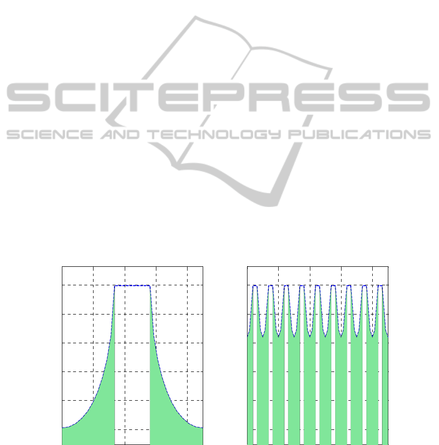
One reason leading to such a difference might be
the lower hole injection into the unshaded parts of
the active layer in the LED A. Thus, the charge-
carrier profile at the interface between the p-GaN
layer and the MQW region was investigated and is
shown in Figure 4. This profile is taken at a higher
voltage than the one corresponding to the IQE peak
value. In such situation, the space-charge-region
(SCR) width becomes extremely small and the
region’s edges move towards the interfaces of the
MQW region. The hole concentration at the
interface p-layer/MQW can be considered
proportional to the hole-current density.
The hole-concentration profile at the interface is
represented by the curve, while the parts
corresponding to the unshaded areas are marked by
the color. They clearly show that the hole
concentration in the areas situated right below the
cathodes (blank areas) is significantly higher than
that in the other areas. This phenomenon can be
explained by the fact that the areas shaded by the
cathodes benefit from a direct hole-injection under
the influence of a strong electric field, whereas in
the unshaded areas the injected-hole concentration is
only slightly raised by the spreading phenomenon.
At this interface, the electric field due to the lattice
mismatch between the p-GaN layer and the InGaN
quantum well and the spontaneous polarization of
GaN altogether hinder the hole injection into the
active region. The strong electric field under the
shaded area reduces this polarization-induced field
better than that in the unshaded areas. This fact also
implies that a large part of the luminous intensity is
lost because the radiative-recombination must be
strongest in those shaded areas.
The average hole concentration in the unshaded
areas is higher in the multiple-cathode LED B than
in the single-cathode LED A. Indeed, at this
interface, the average hole-concentration in the
unshaded areas is 1.72 × 10
15
cm
–3
in the LED A and
1.23 × 10
16
cm
–3
in the LED B, meaning that the hole
injection is more efficient in the LED B.
Furthermore, the average electric-field intensity in
those unshaded parts of the interface is directed
towards the p-GaN layer with values of 66 kV/cm
and 25 kV/cm in the LED A and the LED B
respectively. Consequently, the hole transport is
further hampered in the LED A than in the LED B,
resulting in a lower hole concentration in the active
area.
Figure 3: The simulation results from the LED A (black solid line) and the LED B (blue solid line), respectively a)
Efficiency, b) Normalized efficiency, c) J-V characteristic curve and d) L-V curve.
0 10 20 30 40 50
0
0.2
0.4
0.6
0.8
Current Density (A/cm
2
)
IQE (Arbitrary Unit)
(a) IQE
LED A
LED B
0 10 20 30 40 50
0
0.2
0.4
0.6
0.8
1
Current Density (A/cm
2
)
Normalized IQE
(b) Normalized IQE
LED A
LED B
0 1 2 3 4
10
0
10
5
Voltage (V)
Current Density (A/cm
2
)
(c) J-V
LED A
LED B
0 1 2 3 4
10
0
10
5
Voltage (V)
Optical Power Density (W/cm
2
)
(d) Optical Power Density
LED A
LED B
PHOTOPTICS2015-DoctoralConsortium
42
At the interface between the n-type layer and the
MQW region, the electron-concentration profile (not
shown here) resembles to the above-mentioned hole-
concentration. The average electron-concentrations
in the unshaded areas are respectively
0.76 × 10
16
cm
–3
and 2.62 × 10
16
cm
–3
in the LED A
and the LED B. However, the average electric-field
intensities are approximately equivalent:
5.4 × 10
5
V/cm in LED A and 5.9 × 10
5
V/cm in
LED B.
The injected-hole concentration in the LED B is
more than seven times higher than that in the
LED A, while the same ratio for the injected-
electron concentration between these LEDs is
approximately 3.5. Thus, we suspect that the p-type
layer plays a major role in LED current-injection
and particularly in balancing the charge ratio.
Moreover, as shown by Figure 5, the local injected-
electron/injected-hole ratio is much higher in the
LED A than in the LED B, even reaching values as
high as 45 at the structure’s edges. This ratio in the
LED B consistently fluctuates at around 2,
suggesting that the carrier concentration profile
tends towards an equilibrium which may reduce the
unbalanced charge-ratio and consequently the carrier
leakage. Such values are remarkable as both
structures do not have any electron-blocking layer
and the ionized-donor concentration in the n-type
layer is higher than the ionized-acceptor
concentration in the p-type layer. Furthermore, this
local ratio increases as the distance from the contact
edge increases, while the carrier concentration and
the local current-density decrease. This observation
implies that in this type of LED structure, the
electrode spacing is critical since if it is not well
implemented it can induce areas where poor and
unbalanced carrier-injection occurs. This
problematic should be very critical in the
conventional-chip structure where the mesa length
must be taken into account during LED design, as
remarked by (Huang et al., 2013).
6.4 Overview
Experimental measurements and simulations on
LEDs with two different cathode-structures have
been realized. The characterization and simulation
results show a strong correlation and demonstrate an
improvement in the LED internal-quantum-
efficiency by optimizing the current injection into
the active region. This injection optimization is
critical in LED design as it affects the injected-
carrier concentration-ratio at the active-region edges
and in respect of this ratio variation, the carrier
leakage can be either reduced or intensified. The
simulations also indicate an important role of the
LED p-type-layer in the current injection and,
consequently, in the IQE droop. The employment of
the multiple-stripe-like cathode-structure slightly
varies the electron injection and the electric field
from the n-side of the active region, but strongly
modulates those from the p-side. These unbalanced
injection-induced influences tend to imply a major
Figure 4: Hole-concentration profile at the p-layer/MQW-region interface (left: LED A, right: LED B) at a voltage higher
than that corresponding to the peak IQE value. It implies that the total colored-surface is higher in the LED B than in the
LED A.
0 200 400 600 800
14
14.5
15
15.5
16
16.5
Position (µm)
log
10
(hole concentration) (cm
-3
)
LED B
0 200 400 600 800
14
14.5
15
15.5
16
16.5
Position (µm)
log
10
(hole concentration) (cm
-3
)
LED A
DecorrelationoftheLight-emitting-DiodeInternal-quantum-EfficiencyComponents-StudiesoftheElectron-hole
Concentration-ratioattheActive-regionEdge
43
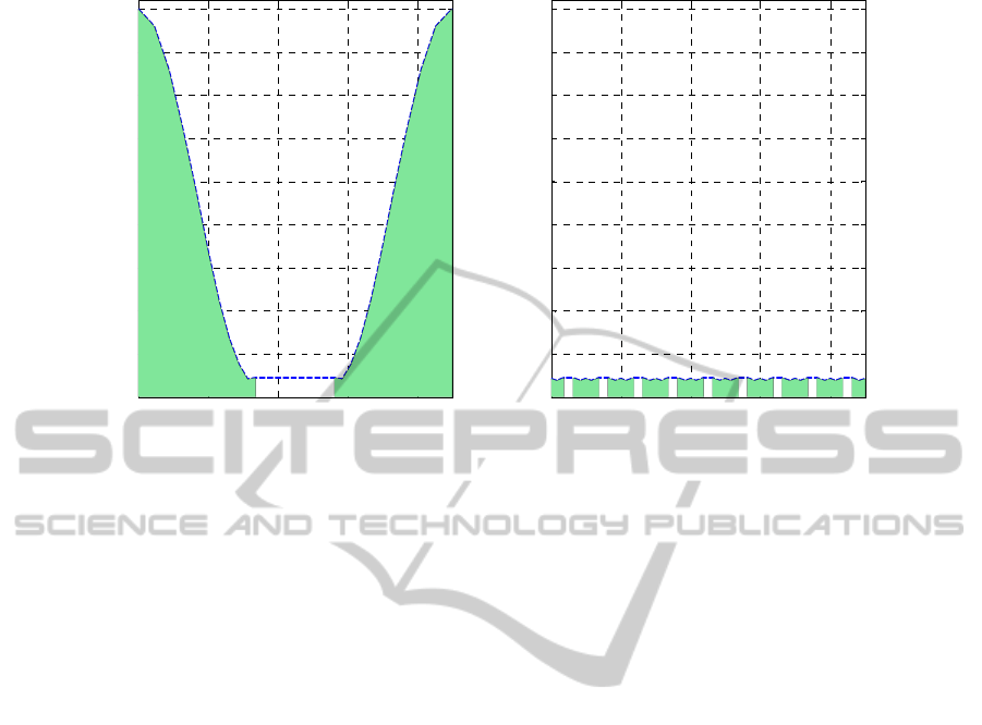
Figure 5: The local injected-electron/injected-hole into the active region at a voltage higher than that corresponding to the
peak IQE for the LED A (left) and the LED B (right). The LED A shows a much more unbalanced local-carrier-profile-ratio
than the LED B and is seemingly more prone to the carrier leakage.
impact of the carrier leakage and perhaps a lesser
role of the Auger-recombination processes in the
IQE droop of LEDs without electron-blocking layer.
It should be noted that, as stated at the beginning, in
the simulations, the SRH carrier-lifetime and the
Auger coefficient were intentionally chosen in order
for the SRH-recombination rate to be reduced and
for the Auger-recombination rate to be amplified.
Several recent results (not detailed in this paper)
suggested that the IQE curve and peak do not
coincide with those of the radiative-recombination-
percentage curve. The latter represents the
percentage of the radiative-recombination rate in the
total recombination rate. In addition to the difference
between the electron and hole concentrations at the
edges of the active region, this impact from carrier
leakage may imply that the commonly-used ABC-
model should be applied very carefully to LEDs
without any electron-blocking layer as it usually
assumes that electron and hole concentrations are
equivalent at high injection.
6.5 Perspective
As stated in the previous section, the p-GaN layer
may play a major role in the efficiency loss. To
further understand the p-type-layer impact on the
carrier injection, further experiments are needed to
study its carrier transport properties. Those
properties are expected to be characterized with
respect to the GaN polarity by using several specific
sample-designs. Important parameters such as the
temperature and the electric field will be varied
during the measurements.
Apart from the material characterization, the
pulsed electroluminescence will help establish the
injected-carrier ratio inside an LED under an
electrical excitation. As seen from the simulation
results, this ratio is expected to be unbalanced,
especially in LEDs without any electron-blocking-
layer. The data acquisition is still ongoing and will
soon be followed by the data-processing phase.
The obtained results are expected to be
communicated soon and contribute to the
decorrelation of the IQE components.
ACKNOWLEDGMENT
This PhD. thesis is funded by the optoelectronic
department (LETI/DOPT) of CEA Grenoble
research center. The author is grateful to the
CNRS/CRHEA for the provided samples.
REFERENCES
Bertazzi, F., Goano, M., Zhou, X., Calciati, M., Ghione,
G., Matsubara, M., Bellotti, E., 2013. Comment on
“Direct Measurement of Auger Electrons Emitted
from a Semiconductor Light-Emitting Diode under
Electrical Injection: Identification of the Dominant
0 200 400 600 800
0
5
10
15
20
25
30
35
40
45
Position (µm)
Ratio e/h
LED B
0 200 400 600 800
0
5
10
15
20
25
30
35
40
45
Position (µm)
Ratio e/h
LED A
PHOTOPTICS2015-DoctoralConsortium
44

Mechanism for Efficiency Droop” [Phys. Rev. Lett.
110, 177406 (2013)].
Cabalu, J.S., Thomidis, C., Moustakas, T.D., Riyopoulos,
S., Zhou, L., Smith, D.J., 2006. Enhanced internal
quantum efficiency and light extraction efficiency
from textured GaN⁄AlGaN quantum wells grown by
molecular beam epitaxy. J. Appl. Phys. 99, 064904.
doi:10.1063/1.2179120.
Cao, X.A., Arthur, S.D., 2004. High-power and reliable
operation of vertical light-emitting diodes on bulk
GaN. Appl. Phys. Lett. 85, 3971.
doi:10.1063/1.1810631.
David, A., Grundmann, M.J., Kaeding, J.F., Gardner, N.F.,
Mihopoulos, T.G., Krames, M.R., 2008. Carrier
distribution in (0001)InGaN⁄GaN multiple quantum
well light-emitting diodes. Appl. Phys. Lett. 92,
053502. doi:10.1063/1.2839305.
Delaney, K.T., Rinke, P., Van de Walle, C.G., 2009.
Auger recombination rates in nitrides from first
principles. Appl. Phys. Lett. 94, 191109.
doi:10.1063/1.3133359.
Della Sala, F., Di Carlo, A., Lugli, P., Bernardini, F.,
Fiorentini, V., Scholz, R., Jancu, J.-M., 1999. Free-
carrier screening of polarization fields in wurtzite
GaN/InGaN laser structures. Appl. Phys. Lett. 74,
2002. doi:10.1063/1.123727.
Galler, B., Drechsel, P., Monnard, R., Rode, P., Stauss, P.,
Froehlich, S., Bergbauer, W., Binder, M., Sabathil, M.,
Hahn, B., Wagner, J., 2012. Influence of indium
content and temperature on Auger-like recombination
in InGaN quantum wells grown on (111) silicon
substrates. Appl. Phys. Lett. 101, 131111.
doi:10.1063/1.4754688.
Hader, J., Moloney, J.V., Pasenow, B., Koch, S.W.,
Sabathil, M., Linder, N., Lutgen, S., 2008. On the
importance of radiative and Auger losses in GaN-
based quantum wells. Appl. Phys. Lett. 92, 261103.
doi:10.1063/1.2953543.
Hangleiter, A., Hitzel, F., Netzel, C., Fuhrmann, D.,
Rossow, U., Ade, G., Hinze, P., 2005. Suppression of
Nonradiative Recombination by V-Shaped Pits in
GaInN/GaN Quantum Wells Produces a Large
Increase in the Light Emission Efficiency. Phys. Rev.
Lett. 95. doi:10.1103/PhysRevLett.95.127402.
Huang, S., Fan, B., Chen, Z., Zheng, Z., Luo, H., Wu, Z.,
Wang, G., Jiang, H., 2013. Lateral Current Spreading
Effect on the Efficiency Droop in GaN Based Light-
Emitting Diodes. J. Disp. Technol. 9, 266–271.
doi:10.1109/JDT.2012.2225092.
Iveland, J., Martinelli, L., Peretti, J., Speck, J.S.,
Weisbuch, C., 2013. Direct Measurement of Auger
Electrons Emitted from a Semiconductor Light-
Emitting Diode under Electrical Injection:
Identification of the Dominant Mechanism for
Efficiency Droop. Phys. Rev. Lett. 110.
doi:10.1103/PhysRevLett.110.177406.
Kim, H., Cho, J., Lee, J.W., Yoon, S., Kim, H., Sone, C.,
Park, Y., Seong, T.-Y., 2007. Measurements of current
spreading length and design of GaN-based light
emitting diodes. Appl. Phys. Lett. 90, 063510.
doi:10.1063/1.2450670.
Kim, M.-H., Schubert, M.F., Dai, Q., Kim, J.K., Schubert,
E.F., Piprek, J., Park, Y., 2007. Origin of efficiency
droop in GaN-based light-emitting diodes. Appl. Phys.
Lett. 91, 183507. doi:10.1063/1.2800290.
Kioupakis, E., Rinke, P., Delaney, K.T., Van de Walle,
C.G., 2011. Indirect Auger recombination as a cause
of efficiency droop in nitride light-emitting diodes.
Appl. Phys. Lett. 98, 161107. doi:10.1063/1.3570656.
Krames, M.R., Christenson, G., Collins, D., Cook, L.W.,
Craford, M.G., Edwards, A., Fletcher, R.M., Gardner,
N.F., Goetz, W.K., Imler, W.R., Johnson, E., Kern,
R.S., Khare, R., Kish, F.A., Lowery, C., Ludowise,
M.J., Mann, R., Maranowski, M., Maranowski, S.A.,
Martin, P.S., O’Shea, J., Rudaz, S.L., Steigerwald,
D.A., Thompson, J., Wierer, J.J., Yu, J., Basile, D.,
Chang, Y.-L., Hasnain, G., Heuschen, M., Killeen,
K.P., Kocot, C.P., Lester, S., Miller, J.N., Mueller,
G.O., Mueller-Mach, R., Rosner, S.J., Schneider, J.,
Richard P., Takeuchi, T., Tan, T.S., 2000. High-
brightness AlGaInN light-emitting diodes. pp. 2–12.
doi:10.1117/12.382822.
Krames, M.R., Shchekin, O.B., Mueller-Mach, R.,
Mueller, G.O., Zhou, L., Harbers, G., Craford, M.G.,
2007. Status and Future of High-Power Light-Emitting
Diodes for Solid-State Lighting. J. Disp. Technol. 3,
160–175. doi:10.1109/JDT.2007.895339.
Li, C.-K., Wu, Y.-R., 2012. Study on the Current
Spreading Effect and Light Extraction Enhancement of
Vertical GaN/InGaN LEDs. IEEE Trans. Electron
Devices 59, 400–407.
doi:10.1109/TED.2011.2176132.
Morkoç, H., 2008. Handbook of nitride semiconductors
and devices. Wiley-VCH ; John Wiley, distributor],
Weinheim : [Chichester.
Mukai, T., Yamada, M., Nakamura, S., 1999.
Characteristics of InGaN-Based
UV/Blue/Green/Amber/Red Light-Emitting Diodes.
Jpn. J. Appl. Phys. 38, 3976–3981.
doi:10.1143/JJAP.38.3976.
Ni, X., Fan, Q., Shimada, R., Özgür, U., Morkoç, H.,
2008. Reduction of efficiency droop in InGaN light
emitting diodes by coupled quantum wells. Appl.
Phys. Lett. 93, 171113. doi:10.1063/1.3012388.
Piprek, J., Farrell, R., DenBaars, S., Nakamura, S., 2006.
Effects of built-in polarization on InGaN-GaN
vertical-cavity surface-emitting lasers. IEEE Photonics
Technol. Lett. 18, 7–9. doi:10.1109/LPT.2005.860045.
Romanowski, Z., Kempisty, P., Sakowski, K., Stra̧ k, P.,
Krukowski, S., 2010. Density Functional Theory
(DFT) Simulations and Polarization Analysis of the
Electric Field in InN/GaN Multiple Quantum Wells
(MQWs). J. Phys. Chem. C 114, 14410–14416.
doi:10.1021/jp104438y.
Rozhansky, I.V., Zakheim, D.A., 2007. Analysis of
processes limiting quantum efficiency of AlGaInN
LEDs at high pumping. Phys. Status Solidi A 204,
227–230. doi:10.1002/pssa.200673567.
Schubert, M.F., Chhajed, S., Kim, J.K., Schubert, E.F.,
DecorrelationoftheLight-emitting-DiodeInternal-quantum-EfficiencyComponents-StudiesoftheElectron-hole
Concentration-ratioattheActive-regionEdge
45

Koleske, D.D., Crawford, M.H., Lee, S.R., Fischer,
A.J., Thaler, G., Banas, M.A., 2007. Effect of
dislocation density on efficiency droop in GaInN⁄GaN
light-emitting diodes. Appl. Phys. Lett. 91, 231114.
doi:10.1063/1.2822442.
Schubert, M.F., Xu, J., Kim, J.K., Schubert, E.F., Kim,
M.H., Yoon, S., Lee, S.M., Sone, C., Sakong, T., Park,
Y., 2008. Polarization-matched GaInN⁄AlGaInN
multi-quantum-well light-emitting diodes with
reduced efficiency droop. Appl. Phys. Lett. 93,
041102. doi:10.1063/1.2963029.
Son, J.H., Kim, B.J., Ryu, C.J., Song, Y.H., Lee, H.K.,
Choi, J.W., Lee, J.-L., 2012. Enhancement of wall-
plug efficiency in vertical InGaN/GaN LEDs by
improved current spreading. Opt. Express 20, A287.
doi:10.1364/OE.20.00A287.
Thompson, G.H.B., 1980. Physics of semiconductor laser
devices. J. Wiley, Chichester [Eng.] ; New York.
Turin, V.O., 2005. A modified transferred-electron high-
field mobility model for GaN devices simulation.
Solid-State Electron. 49, 1678–1682.
doi:10.1016/j.sse.2005.09.002.
Xu, J., Schubert, M.F., Noemaun, A.N., Zhu, D., Kim,
J.K., Schubert, E.F., Kim, M.H., Chung, H.J., Yoon,
S., Sone, C., Park, Y., 2009. Reduction in efficiency
droop, forward voltage, ideality factor, and
wavelength shift in polarization-matched
GaInN/GaInN multi-quantum-well light-emitting
diodes. Appl. Phys. Lett. 94, 011113.
doi:10.1063/1.3058687.
Zhang, Z.-H., Ju, Z., Liu, W., Tan, S.T., Ji, Y., Kyaw, Z.,
Zhang, X., Hasanov, N., Sun, X.W., Demir, H.V.,
2014. Improving hole injection efficiency by
manipulating the hole transport mechanism through p-
type electron blocking layer engineering. Opt. Lett. 39,
2483. doi:10.1364/OL.39.002483.
PHOTOPTICS2015-DoctoralConsortium
46
