
Amorphous Ge-As-Te Thin Films Prepared by Pulsed Laser
Deposition
A Photostability Study
M. Bouška
1
, P. Hawlová
1
, V. Nazabal
1,2
, L. Beneš
3
and and P. Němec
1
1
Department of Graphic Arts and Photophysics, Faculty of Chemical Technology, University of Pardubice,
53210, Pardubice, Czech Republic
2
Institut des sciences chimuques de Rennes, UMR CNRS 6226, Equipe Verres et Céramiques,
Université de Rennes 1, 35042, Rennes, France
3
Joint Laboratory of Solid State Chemistry of the Institute of Macromolecular Chemistry AS CR,
v.v.i. and University of Pardubice, Studentská 84, 53210, Pardubice, Czech Republic
Keywords: Amorphous Chalcogenide, Thin Films, Ge-As-Te, Photostability.
Abstract: Pulsed laser deposition was used for the fabrication of amorphous thin films from Ge-As-Te system with the
aim to study their intrinsic photostability. Photostability of prepared layers was studied using spectroscopic
ellipsometry within as-deposited as well as relaxed layers. For irradiation, laser sources operating at three
energies (1.17, 0.92 and 0.8 eV) in band gap region of the studied materials were employed. The lowest
values of photorefraction (refractive index changes) accompanied with lowest changes of band gap values
present Ge
20
As
20
Te
60
thin films, which are therefore considered as the layers with highest photostability,
especially in relaxed state.
1 INTRODUCTION
Amorphous chalcogenides based on S, Se and Te
elements in combination with suitable element(s)
from 14
th
or 15
th
group of periodical system
(typically Ge, As, etc.) are unique due to their
photoinduced phenomena. Irradiation with
appropriate energy and intensity may change
physico-chemical properties (refractive index, band
gap, thickness, etc.) of amorphous chalcogenide thin
films (Shimakawa et al., 1995). On the other hand,
photoinduced changes of structure and properties
limit potential applications of amorphous
chalcogenides in the field of infrared optics based on
their interesting nonlinear optical properties
(Chauvet et al., 2009).
Knowledge of photoinduced phenomena in
binary arsenic- and germanium-based amorphous
chalcogenides (Nemec et al., 2009; Sleecky et al.,
1996; Vateva, 2007) suggests that in ternary Ge-As-
Te(S, Se) materials, photodarkening (decrease of
band gap energy) and photobleaching (increase of
band gap energy), connected with positive or
negative photorefraction (refractive index changes),
could be compensated by an appropriate choice of
composition. Nevertheless, the studies leading to
optimization of intrinsic chemical composition of
amorphous chalcogenides in order to prevent
undesired photoinduced effects are rare (Yang et al.,
2008; Nemec et al., 2010; Su et al., 2013), focusing
on Ge-As-Se thin amorphous films.
Transmission window of S- and Se-based
amorphous chalcogenides in infrared is restricted by
the long-wavelength (multiphonon) absorption edge
at 11 and 15 µm, respectively (Eggleton at al.,
2011). Nevertheless, for some applications, it is
necessary to develop materials optically transparent
beyond 16 µm. This requirement might be satisfied
by use of amorphous tellurides, for example from
binary Te-X (X = Cl, Br or I), Ge-Te, As-Te or
ternary Ge-Ga-Te, Ge-Te-I, Ge-In-Te or Ge-As-Te
systems (Bureau et al., 2008; Yang and Lucas,
2009). Excellent optical transparency in the 3–20
µm spectral window as well as large refractive index
values (>3.5 at 1.55 µm) were reported for Ge-As-
Te glasses (Yang and Lucas, 2009; Hawlova et al.,
2014).
Based on interesting bulk glasses properties and
expectation of photostable thin films discovery, this
work deals with amorphous thin films from Ge-As-
103
Bouška M., Hawlová P., Nazabal V., Beneš L. and N
ˇ
emec P..
Amorphous Ge-As-Te Thin Films Prepared by Pulsed Laser Deposition - A Photostability Study.
DOI: 10.5220/0005338301030107
In Proceedings of the 3rd International Conference on Photonics, Optics and Laser Technology (PHOTOPTICS-2015), pages 103-107
ISBN: 978-989-758-092-5
Copyright
c
2015 SCITEPRESS (Science and Technology Publications, Lda.)
Te system. Specifically, the aim of this work is to
find Ge-As-Te photostable thin films in as-deposited
but preferably in relaxed (annealed) state. The term
photostability is defined here as insensitivity of the
material to light exposure in terms of constant values
of refractive index and optical band gap.
For the fabrication of Ge-As-Te amorphous thin
films, electron beam or flash evaporation was
already used (Eggleton at al., 2011; Bureau et al.,
2008). In this work, we used pulsed laser deposition
(PLD) for thin films growth. We have already shown
that PLD technique seems to be promising for
chalcogenide thin films fabrication due to its
simplicity, easy control of the deposition process,
possibility to fabricate multilayered structures and
often stoichiometric material transfer from the target
to the films (Yang and Lucas, 2009; Hawlova et al.,
2014).
Following our previous studies in Ge-As-Se
system (Nemec et al., 2010; S. H. Mohamed et al.,
2006), in this work we studied photostability/
photosensitivity for six selected compositions from
Ge-As-Te system employing three different laser
sources with photon energy close to band gap of
studied materials (amorphous chalcogenides are
generally most sensitive for exposures with band gap
light). Five compositions followed the trend of
increasing mean coordination number (MCN) from
2.4 to 2.8; last composition (Ge
20
As
20
Te
60
,
MCN=2.6) was selected for a comparison with Ge-
As-Se system studied recently.
2 RESULTS
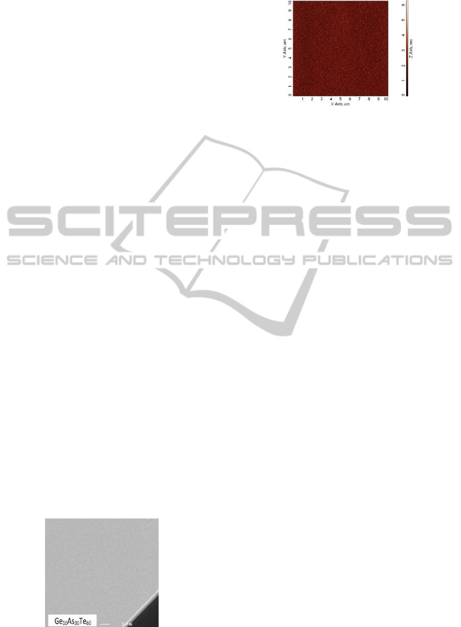
Thin films fabricated by PLD were amorphous and
homogenous according XRD patterns and SEM. The
SEM and AFM data showed smooth surface of thin
films, without cracks and corrugations (Fig. 1 and
2).
We observed only rarely sub-micrometer sized
droplets. Surface roughness (RMS) values of all thin
films determined by AFM were found to be lower
Figure 1: SEM micrograph of Ge
10
As
30
Te
60
thin film.
Figure 2: AFM of as-deposited Ge
10
As
50
Te
40
thin film.
than ~1.7 nm; no changes in surface roughness
values were indicated for annealed, irradiated and
post-annealing irradiated layers.
The chemical composition of fabricated layers,
as determined by SEM-EDS, is in good agreement
with the composition of used bulk targets (Hawlova
et al., 2014). The only exception is Ge
10
As
60
Te
30
composition, where the differences between thin
film and bulk target composition are probably
caused by non-homogeneity of the starting bulk
material, which was partly crystalline. In spite of the
fact that the bulk Ge
20
As
20
Te
60
target was
completely crystalline (this composition is located
outside the glass-forming region (Krebs and Fischer,
1970)), corresponding films were amorphous and
their chemical composition agreed well with average
composition of the used target.
Two series of Ge
x
As
y
Te
100-x-y
thin films differing
in thickness (~ 270-375 and ~810-1050 nm, Table 1)
were fabricated in order to satisfy criterion of
penetration depth of the light sources used for the
exposure experiments which must be equal or larger
than the film thickness. The penetration depth
(1/abs. coef.) for 1064 nm (1.17 eV) laser light was
estimated to be 300-400 nm, light from two other
sources had penetration depth values larger than
2 µm. Because films with thickness around 300 nm
were irradiated with 1342 nm (0.92 eV) laser and
films with thickness around 1000 nm were exposed
with 1342 nm (0.92 eV) sources, above mentioned
criterion is considered as satisfied.
The thicknesses, optical band gap and refractive
indices of all thin films were determined by variable
angle spectroscopic ellipsometry (VASE) data
analysis. The applicability of used Cody-Lorentz
model for the VASE data analysis is confirmed by
low values of mean square error (MSE) of the fitting
procedure, typically MSE<6.
Table 1 show optical band gap values and
refractive indices at 1540 nm for 300 nm PLD Ge-
As-Te thin films in different states (as-deposited,
exposed, annealed, post-annealing exposed). The
data presented stand for irradiation with laser
PHOTOPTICS2015-InternationalConferenceonPhotonics,OpticsandLaserTechnology
104

sources operating at 1342 nm (0.92 eV, band gap
light). Data for ~1000 nm films and other irradiation
experiments were also obtained but they are not
shown in Table 1 for clarity.
3 DISCUSSION
Performed experiments and data analysis show that
the irradiation of as-deposited Ge-As-Te layers leads
to some photodarkening effect for ~300 nm thick
films with nominal composition Ge
10
As
20
Te
70
(partly
also Ge
10
As
30
Te
60
); the photodarkening takes place
for 0.92 eV irradiation (ΔE
g
opt
up to ~0.11 eV).
Under 1.17 eV exposure, films are photostable. For
~1000 nm thick films, the impact of irradiation on
as-deposited films has following trend. Under
0.92 eV irradiation, clear photobleaching was
observed for most of the samples (ΔE
g
opt
up to
~0.07 eV). On the other hand, under 0.8 eV
irradiation, only weak photobleaching was detected
for Ge
10
As
40
Te
50
and Ge
10
As
50
Te
40
layers (ΔE
g
opt
up
to ~0.04 eV), if any. Exposure of as-deposited Ge-
As-Te films has generally only small effect on their
refractive index values at 1540 nm, if any
(Δn ≤ 0.02).
The relaxation of as-deposited films via
annealing in inert atmosphere generally results in
their bleaching (ΔE
g
opt
up to ~0.18 eV for
Ge
10
As
60
Te
30
), excluding 300 nm Ge
10
As
20
Te
70
layers which underwent darkening (ΔE
g
opt
up to
~0.07 eV). The bleaching of as-deposited thin films
due to annealing is connected with the decrease of
refractive index (Δn up to ~0.16 in case of
Ge
10
As
60
Te
30
).
The behavior of relaxed (annealed) PLD Ge-As-
Te amorphous thin films under exposure with
different laser sources has not general trends (except
the fact that no photobleaching was identified); that
is why each composition will be commented
separately. Two compositions (Ge
10
As
50
Te
40
and
Ge
20
As
20
Te
60
) exhibit almost completely photostable
behavior of optical band gap in relaxed state.
Relaxed Ge
10
As
20
Te
70
layers show photodarkening
reaching ΔE
g
opt
up to ~0.09 eV for 0.92 eV
irradiation. Photodarkening was observed also for
Ge
10
As
30
Te
60
relaxed films; ΔE
g
opt
~0.08 eV for 0.92
eV irradiation, magnitude of photodarkening is
lower for two other irradiation sources. In case of
Ge
10
As
40
Te
50
annealed films, photostability was
found for 1.17 eV exposures; contrary, for 0.92 and
0.80 eV irradiation, weak photodarkening is
reported. Finally, the photostability of Ge
10
As
60
Te
30
layers in relaxed state is rather good under 1.17 and
0.92 eV irradiation; however, under 0.80 eV
exposure photodarkening with magnitude of ΔE
g
opt
~0.05 eV is seen. From the point of photorefraction,
four studied compositions (Ge
10
As
30
Te
60
,
Ge
10
As
40
Te
50
, Ge
10
As
50
Te
40
and Ge
20
As
20
Te
60
)
present almost zero photorefraction in relaxed state
under all three irradiation sources.
Taking into account all the data, lowest values of
photorefraction accompanied with lowest changes of
band gap values were identified for Ge
20
As
20
Te
60
thin films, which are therefore considered as the
layers with highest photostability among studied
samples, especially in relaxed state. Zero
photorefraction is of high importance for some
applications of amorphous chalcogenides, such as
for laser beam propagation in nonlinear regime
(Chauvet et al., 2009). That is why pulsed laser
deposited Ge
20
As
20
Te
60
thin films are attractive; they
are promising also due to their expected high
(non)linear refractive index.
Table 1: Optical band gap values (in eV) and refractive indices (at 1540 nm) of Ge-As-Te thin films at different stages of
the experiments (as-deposited, exposed, annealed and post-annealing exposed). Exposure experiments were performed with
0.92 eV CW laser source. Band gap values (± 0.01 eV), refractive index data (± 0.01) as well as thicknesses (± 2 nm) of two
series of fabricated films were extracted from VASE data analysis. MCN stands for the mean coordination numbers
calculated from chemical composition of the films measured by EDS. Note that data shown are for films with ~300 nm
thickness.
Nominal composition MCN Thickness (nm) Optical band gap (eV) Refractive index
as-deposited annealed as-deposited annealed
non-irrad./irrad non-irrad./irrad non-irrad./irrad non-irrad./irrad
Ge
10
As
20
Te
70
2.50 280/1050 0.90/0.79 0.86/0.77 3.76/3.76 3.75/3.74
Ge
10
As
30
Te
60
2.53 270/870 0.89/0.84 0.96/0.88 3.69/3.68 3.67/3.66
Ge
10
As
40
Te
50
2.63 320/810 0.90/0.90 0.99/0.95 3.71/3.70 3.61/3.62
Ge
10
As
50
Te
40
2.72 335/930 0.90/0.90 1.00/1.01 3.70/3.69 3.59/3.57
Ge
10
As
60
Te
30
2.74 375/1000 0.89/0.89 1.07/1.07 3.68/3.66 3.52/3.52
Ge
20
As
20
Te
60
2.64 330/1010 0.90/0.89 1.01/1.00 3.63/3.63 3.53/3.52
AmorphousGe-As-TeThinFilmsPreparedbyPulsedLaserDeposition-APhotostabilityStudy
105

Discovery of thin films photostability in Ge-As-Te
system, located at Ge
20
As
20
Te
60
composition
(MCN=2.6), is coherent with our earlier work
dealing with Ge-As-Se amorphous layers, where the
photostable composition was found to be
Ge
20
As
20
Se
60
(Nemec et al., 2010). As pointed out by
Calvez et al. (2008), photostructural changes such as
photodarkening decrease and tend to vanish in
overcoordinated glasses, i.e. when MCN= 2.6 in Ge-
As-Se system. In case of Ge-As-Te thin films
studied here, some compositions have MCN higher
than 2.6; however, they present some photoinduced
phenomena. Moreover, Ge
10
As
40
Te
50
films having
MCN=2.6 are not completely photostable. Above
mentioned facts lead to the conclusion that MCN
does not seem to be the main decisive parameter
influencing photostability of amorphous
chalcogenides. Our conclusion is supported by the
work of Khan et al., who studied light induced
response of thermally evaporated Ge-As-Se thin
films concluding that coexisting photodarkening and
photobleaching do not show a regular trend with
respect to MCN; instead evidence that Ge: As ratio
plays important role, rather than rigidity of the
amorphous network, is provided (Khan et al., 2014).
In summary, pulsed laser deposition was
exploited for the fabrication of Ge-As-Te amorphous
thin films. Morphology of prepared films is of good
quality and their surface roughness is low.
Photostability of the layers was studied in as-
deposited as well as annealed state of the samples
under irradiation with lasers operating at 1064, 1342
and 1550 nm. Highest photostability was found for
Ge
20
As
20
Te
60
thin films, which are therefore
promising for nonlinear applications.
4 METHODS
4.1 Samples Preparation
The targets used for PLD were bulk chalcogenide
materials with nominal composition Ge
10
As
20
Te
70
,
Ge
10
As
30
Te
60
, Ge
10
As
40
Te
50
, Ge
10
As
50
Te
40
,
Ge
10
As
60
Te
30
and Ge
20
As
20
Te
60
. Bulk samples were
prepared by weighting high purity elements (5-6 N)
in fused silica ampoules which were evacuated for a
few hours and sealed subsequently. The sealed
ampoules were heated in a rocking furnace at 1050C
for 12 hours and then quenched in water. Finally,
glass rods were cut and polished for targets useful
for PLD.
4.2 Thin Films Fabrication
For fabrication of thin films, a KrF excimer laser
operating in UV (248 nm) was used. The laser
pulses had constant output energy of 300 ± 3 mJ per
pulse, 30 ns pulse duration and 20 Hz repetition rate.
The energy fluency was set at ~ 2.6 J.cm
-2
. Vacuum
chamber (residual pressure < 3x10
-4
Pa) was used
for the fabrication of thin films; substrates were
chemically cleaned microscope glass slides and Si
wafers. The substrates were positioned parallel to
the target at target-to-substrate distance of 5 cm.
Off-axis PLD technique with rotating target and
substrates was used to avoid deep damage of the
target and to improve the thickness homogeneity of
deposited thin films.
4.3 Photostability Experiments
Photostability was studied with as-deposited and
annealed thin films. The annealing was realized in
inert atmosphere of pure argon; annealing
temperature was 20 °C below the respective glass
transition temperature of the corresponding target
glass (Hawlova et al., 2014). The duration of
annealing was 120 min; the samples were
consequently slowly cooled down to room
temperature at 1 °C.min
-1
. The photostability
experiments were performed via exposure of thin
films by laser sources operating at 1064 nm
(1.17 eV), 1342 nm (0.92 eV) and 1550 nm
(0.80 eV) with intensity of ~160 mW.cm
-2
for
exposure time long enough (120 min) for the
saturation of the photoinduced phenomena, if any.
Laser exposures were realized in inert nitrogen
atmosphere to avoid the oxidation of the films
during the experiments.
4.4 Morphological, Compositional and
Structural Characterization
A scanning electron microscope with energy-
dispersive X-ray analyser (SEM-EDS, JSM 6400-
OXFORD Link INCA) was used for chemical
composition determination of prepared Ge-As-Te
films. SEM technique was also applied to observe
the morphology of thin films using a field-emission
gun SEM (JMS 6301F). X-ray diffraction (XRD)
technique (D8-Advance diffractometer, Bruker
AXS) was exploited to prove amorphous state of
thin layers using Bragg–Brentano θ–θ geometry with
CuKα radiation and secondary graphite
monochromator. The diffraction angles were
measured at room temperature from 5 to 65° (2θ) in
PHOTOPTICS2015-InternationalConferenceonPhotonics,OpticsandLaserTechnology
106

0.02° steps with a counting time of 5 s per step.
Atomic force microscopy (AFM, Solver NEXT, NT-
MDT) was used to study topography of Ge-As-Te
thin films within typical scanned area 10 µm × 10 µm
in semicontact mode.
4.5 Optical Characterization
Optical functions (refractive indices and extinction
coefficient spectral dependences) and thicknesses of
Ge-As-Te
thin films were obtained from the analysis
of spectroscopic ellipsometry data measured using
an ellipsometer with automatic rotating analyzer
(VASE, J.A. Woollam Co., Inc.) The measurement
parameters are as follows: spectral region
300–2300 nm with 10 or 20 nm steps (depending on
thickness of the films), angles of incidence 50°, 60°
and 70°. For the analysis of VASE data we used
Cody-Lorentz model (Cody, 1984), which includes
the correct band edge function, weak Urbach
absorption tail description as well as Lorentz
oscillator function; this model is appropriate for the
description of amorphous chalcogenides optical
functions and their photo-induced changes (Nemec
et al., 2010).
ACKNOWLEDGEMENTS
The Czech Science Foundation (Project No.
13-05082S), Ministry of Education, Youth and
Sports of the Czech Republic (Project
CZ.1.07/2.3.00/30.0058) and the CNRS PICS
(Projet International de Cooperation Scientifique)
program financially supported this work.
REFERENCES
Bureau, B., Danto, S., Li Ma, H., Boussard-Plédel, C.,
Zhang, X. H., Lucas, J., Solid State Sci. 10, 427-433,
2008.
Calvez, L., Yang, Z. Y., Lucas, P., 2008, Phys. Rev. Lett.
101, 177402.
Cody, G. D., 1984, in Semiconductors and Semimetals
Vol. Volume 21, Part B (ed I. Pankove Jacques) 11-82
(Elsevier).
Eggleton, B. J., Luther-Davies, B., Richardson, K., 2011,
Nature Photonics 5, 141-148.
Hawlova, P., Olivier, M., Verger, F., Nazabal, V., Nemec,
P., 2013, Mater. Res. Bull. 48, 3860-3864.
Hawlová, P., Verger, F., Nazabal, V., Boidin, R. and
Nemec, P., 2014, J. Am. Ceram. Soc., 97, 3044-3047.
Chauvet, M. et al., 2009, Opt. Lett. 34, 1804-1806.
Khan, P., Jain, H., Adarsh, K. V., 2014, Scientific Reports
4, 4029.
Krebs, H., Fischer, P., 1970, Discussions of the Faraday
Society 50, 35-44.
Nemec, P. et al., 2010, Opt. Express 18, 22944-22957.
Nemec, P. et al., 2013, Thin Solid Films 539, 226-232.
Nemec, P., Nazabal, V., Frumar, M., 2009, J. Appl. Phys.
106, 023509.
Nemec, P., Takats, V., Csik, A., Kokenyesi, S., 2008, J.
Non-Cryst. Solids 354, 5421-5424.
Pinto, R., 1971, Thin Solid Films 7, 391-404.
S. H. Mohamed, M. M. Wakkad, A.M. Ahmed, Diab, A.
K., 2006, The European Physical Journal Applied
Physics 34, 165-171.
Shimakawa, K., Kolobov, A., Elliott, S. R., 1995, Adv.
Phys. 44, 475-588.
Sleecky, E., Tichy, L., Nagels, P., Callaerts, R., 1996, J.
Non-Cryst. Solids 200, 723-727.
Su, X., Wang, R., Luther-Davies, B., Wang, L., 2013,
Appl. Phys. A-Mater. Sci. Process. 113, 575-581.
Vateva, E., 2007, J. Optoelectron. Adv. Mater. 9, 3108-
3114.
Yang, G. et al., 2008, Opt. Express 16, 10565-10571.
Yang, Z. Y., Lucas, P., 2009, J. Am. Ceram. Soc. 92,
2920-2923.
AmorphousGe-As-TeThinFilmsPreparedbyPulsedLaserDeposition-APhotostabilityStudy
107
