
Broadband Absorption in the Cavity Resonators with Changed Order
Agata Roszkiewicz
Institute of Fundamental Technological Research, Polish Academy of Sciences,
Adolfa Pawińskiego 5b, 02-106 Warsaw, Poland
Keywords: Broadband Absorption, Enhanced Absorption, Localized Surface Plasmons, Cavity Resonances, Diffraction
Gratings.
Abstract: This paper presents an analysis of phenomena leading to high and broadband absorption at a structure
combined of three elements: one-dimensional dielectric diffraction grating placed between silver grating
and a thick silver substrate. Each element of the dielectric grating consists of media of different dielectric
constants but of the same geometrical dimensions. A broad spectrum of high absorption in such a structure
is achieved as a result of two issues. First, due to the different excitation conditions the cavity resonances
are excited at different wavelengths. Second, the changed order of the resonators leads to further broadening
of the absorption band.
1 INTRODUCTION
High and broadband absorption of electromagnetic
waves is of interest in many nanophotonic
applications. Various kinds of configurations were
proposed to obtain near zero reflection and trapping
of light in the structure. Control of the reflection and
transmission is an important issue especially in
photodetectors and solar cells (Ferry et. al., 2010).
The total absorption of radiation by a metallic
structure has attracted significant interests over the
past few years (Liu et. al., 2010, Shchegolkov et. al.,
2010, Liu et. al., 2011). Many metallodielectric
structures designed as nearly perfect absorbers have
been proposed and some promising applications
have been discussed.
The near perfect absorption may be achieved
with use of localized plasmon resonances (Hu et. al.,
2009, Kravets et. al., 2010, Liu et. al., 2011, Pan et.
al., 2013), gap plasmons in bottle-like cavities
(Meng et. al., 2013), propagating surface plasmon
polaritons (Chen et. al., 2010) or Fabry-Perot
resonances in cavities between two metal surfaces
(Diem et. al., 2009, Hao et. al., 2010, Roszkiewicz
et. al., 2012, Song et. al., 2013). The designs based
on a Fabry-Perot resonance usually are composed of
periodic gratings. In order to obtain a wide
absorption band, each period of the structure can be
made of resonators of varied dimensions, supporting
resonances at different wavelengths (Song et. al.,
2013, Koechlin et. al., 2011, Zhang et. al., 2013,
Wang et. al., 2013). The continuation of such a
structure is a quasiperiodic structure (Dolev et. al.,
2011) and chirped grating with slowly varying
period (Chen et. al., 2010, Bouillard et. al., 2012,
Gan et. al., 2011). In those periodic configurations
the wide absorption band is a result of the existence
of similar resonances occurring at neighbouring
frequencies. However, in those examples all cavities
are filled with the same material and the resonators
are ordered according to their resonance
wavelengths.
In this paper we analyse a one-dimensional (1D)
absorptive structure. The presented configuration is
based on a 1D dielectric diffraction grating placed
between silver grating and a thick silver substrate.
The structure realizes simultaneous suppression of
reflection and transmission, leading to enhanced
absorption. Each element of the dielectric grating
consists of dielectric medium of different dielectric
constant but of the same geometrical dimensions. A
broad spectrum of high absorption in such a
structure is achieved as a result of the horizontal
cavity modes (HCMs) excited at different
wavelengths. Moreover, the changed order of the
resonators leads to further broadening of the
absorption band. It occurs that the sequence of the
resonators influences on the absorption
characteristics at normal as well as oblique
incidence.
81
Roszkiewicz A..
Broadband Absorption in the Cavity Resonators with Changed Order.
DOI: 10.5220/0005332900810086
In Proceedings of the 3rd International Conference on Photonics, Optics and Laser Technology (PHOTOPTICS-2015), pages 81-86
ISBN: 978-989-758-093-2
Copyright
c
2015 SCITEPRESS (Science and Technology Publications, Lda.)
2 SIMULATION MODEL AND
METHOD
The analysed configuration is depicted in figure 1. A
TM polarized plane wave is incident normally from
air at a 1D stacked silver and dielectric gratings with
subwavelength slits placed at the silver substrate.
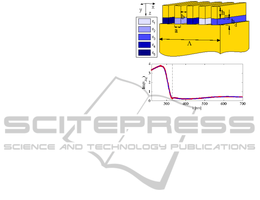
Each period of the structure consists of N = 5
identical metal stripes lying on the dielectric
resonators with different dielectric constants. The
relative change between dielectric constants of the
resonators is denoted by
Δε
. Hence the dielectric
constant of the n
th
stripe (n = 1, 2, ..., N) is
ε
n
=
ε
0
+
n
Δε
, where
ε
0
= 1 is the dielectric constant of air and
Δε
= 0.8. We show, that the optimized structure
does not consist of resonators placed in order
according to the increasing resonance wavelength.
The structure characterized by the widest absorption
band is the structure, where the sequence of the
resonators is:
ε
5
,
ε
2
,
ε
4
,
ε
1
,
ε
3
.
Numerical analysis of the optical response of the
structure was performed with use of Rigorous
Coupled Wave Analysis with implementation of the
scattering matrix algorithm, multilayer extension
and the factorization rules. The dielectric function of
silver was numerically fitted to the experimental
data (Johnson et. al., 1972).
3 SIMULATION RESULTS
It is known that by introducing different resonators
in one structure one can obtain a wide absorption
spectrum due to the excitation of resonances at
different wavelengths. In this paper we utilize the
concept of the 1D grating absorber presented in
figure 1. The main cause of high absorption in this
kind of structure is the excitation of the open metal-
dielectric-metal (MIM) horizontal cavity modes in
those dielectric resonators. The formation of the
cavity mode results in low reflection and strong
absorption, making most of electromagnetic field
focus inside the cavity. However, usually the
resonators are placed in an order accordingly to their
resonance wavelengths (Chen et. al., 2010, Song et.
al., 2013, Bouillard et. al., 2012). Here we change
this order.
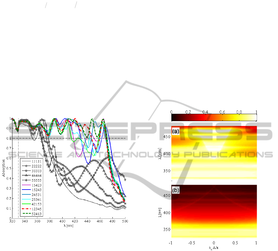
Figure 2 gives the calculated absorption as a
function of the incident wavelength for
configurations with
Δε
= 0.8 and various orders of
dielectric resonators, among others the optimized
structure (green dashed line) and the ordered
configuration (red dashed-dotted line). The plot
Figure 1: (a) Configuration of the analysed problem. One
period of the structure
Λ
= 380 nm is presented. Silver 1D
grating of thickness h
m
= 25 nm is placed on the dielectric
grating of thickness h
d
= 21 nm. Dimensions of the
equally spaced ridges of identical dimensions: a = 30.4
nm, b = 45.6 nm and the filling factor f = 0.4. (b)
Imaginary part of the dielectric function of silver as a
function of wavelength. Blue line – experimental data
from (Johnson et. al., 1972), red dots – numerical fit.
Vertical dashed line denotes
λ
= 330 nm.
shows also the absorption curve for different
configurations with constant
ε
n
for comparison (dark
grey lines). The absorption spectrum differs for
structures with differently arranged resonators, even
under normal incidence. Other sequences of the
same resonators than the optimized one significantly
reduce the absorption bandwidth. It can be seen that
the non-optimized configurations are characterized
by narrower absorption band than the optimal
structure, despite the fact, that all of them consist of
the same resonators, however placed in different
order. Thus it appears, that the sequence of the
dielectric resonators in each grating period is also an
important parameter to be optimized. Moreover, the
maximal amplitudes of the resonances in structures
with constant
ε
n
are at the level of ~60%, hence they
do not assure the high absorption. This behaviour
will be discussed later.
Each cavity resonator can be regarded as two
single metal-insulator interfaces brought close to
each other. In this situation, the dispersion curve of a
single interface splits into high and low-energy
modes. Here, due to the field symmetry matching,
only the low-energy mode is excited. Dispersion
curve for the symmetric mode in each cavity
depends on its dielectric constant
ε
and thickness h
d
and can be described by the relation:
(a)
(b)
PHOTOPTICS2015-InternationalConferenceonPhotonics,OpticsandLaserTechnology
82
()
() ()
()
m
zn
m
zdz
kkhk
εε
−=2tanh
(1)
where k
z
,
ε
n
, k
z
(m)
and
ε
(m)
are the z-components of
the wave vector and the dielectric constants in the
dielectric and metal media, respectively (Maier,
2007). A dispersion curve can be drawn for each
resonator with the consideration of its thickness and
dielectric constant
ε
n
. Points at this dispersion curve
for a given cavity length a
≈
ν
h
λ
p
/2, where ν
h
= 1
denotes the resonance order in the horizontal cavity,
allow to obtain the plasmon resonance wavelength
for the wave vector k = 2
π
/
λ
p
=
π
ν
h
/a. Hence, the
energy in the resonator can be spatially restricted by
metal interfaces (in the vertical direction) and by
large wave vectors of the supported plasmon modes
(in the horizontal direction).
Figure 2: Absorption spectrum as a function of wavelength
for exemplary structures with differently ordered
resonators under normal incidence. Legend shows
configurations of the resonators in each period, green
dashed line and red dashed-dotted line show the
absorption of the optimized structure and the structure
with ordered resonators, respectively. Dark grey lines
show the absorption of the structures with all identical
resonators within the period. Horizontal dashed line
denotes absorption level of 80%. Vertical dashed line
denotes
λ
= 330 nm.
The excitation conditions for cavity modes are
different in each resonator since, having the same
dimensions, the resonators are filled with media of
different dielectric constants. This results in
frequency splitting of the resonance curves
originating from the particular HCMs and thus
widening of the total absorption band. In the
presented configuration those electric dipole
resonances correspond to peaks between 380 – 500
nm wavelength.
High absorption at wavelengths shorter than 330
nm does not originate from any of the plasmonic
resonances. The limit value of the wavelength where
silver is characterized by low inner loss is about 330
nm. For shorter wavelengths the imaginary part of
the dielectric function of silver increases rapidly
(figure 1(b)). Hence, high absorption at wavelengths
lower than 330 nm visible in presented figures arises
from phenomena related to conduction and bound
electrons and it is caused by the interband transitions
of electrons in metal. For this reason the width of the
absorption band is calculated for wavelengths longer
than 330 nm. Resonances between ~330-380 nm are
connected with the excitation of localized surface
plasmons (LSPs), mainly at the metal ridges.
Figure 3: Absorption spectrum as a function of wavelength
and incident wave vector for (a) the optimized structure
and (b) structure with
ε
n
=
ε
1
.
The width of the band of more than 80%
absorption efficiency at normal incidence for the
optimized structure increased of ~121 nm in
comparison to the absorption band of the structure
with
ε
n
=
ε
1
, where n = 1, 2,...,5. Hence, the
absorption band width at normal incidence is
estimated to be ~141 nm, which can be compared
with ~23 nm bandwidth of the
ε
n
=
ε
1
structure. This
gives about 6.1-fold increase of the stop band width
in the optimized structure. Moreover, the bandwidth
of the ordered structure is ~116 nm, which gives
almost 1.2-fold increase of the absorption bandwidth
resulted from the changed order of the resonators.
In order to further analyse the properties of the
BroadbandAbsorptionintheCavityResonatorswithChangedOrder
83
modes responsible for high absorption, in figure 3
we present the absorption spectra as a function of
wavelength and in-plane component of the incident
field wave vector for the optimized structure and the
structure with
ε
n
=
ε
1
. First, it is worth to point out
that all resonances taking part in enhanced
absorption are dispersionless, which excludes
excitation of propagating surface plasmon
polaritons.
Second, since at λ =
Λ
= 380 nm the +/- 1
st
propagating diffraction orders appear, it is of interest
to design the structure so that all the HCMs are
excited at longer wavelengths, in the zero-order
regime, as presented. This prevents from unwanted
loss of energy which, otherwise, is distributed
between the propagating orders and may cause
lowering of the HCMs excitation efficiency.
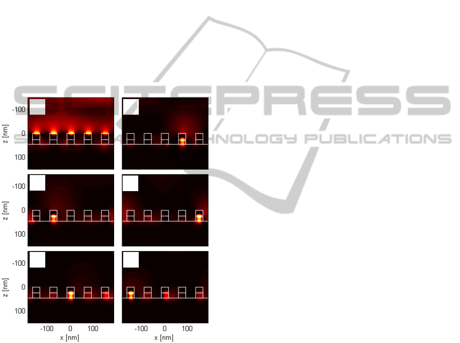
Figure 4: Magnetic field intensity distribution under
normal incidence in one grating period of the optimized
structure at the peak wavelengths: 364, 387, 411, 428, 447
and 465 nm. Colour maps at each plot are scaled
independently.
Third, whilst the LSP resonances at wavelengths
330-380 nm do not exhibit any dependence on the
incidence angle sign, resonances at longer
wavelengths show this dependence. The asymmetry
in absorption is clearly visible at wavelength range
corresponding to the cavity modes. The absorption
remains very high for the illumination in the zero-
order regime, but outside it lowers and shows an
asymmetry withe regard to the incidence angle sign.
This indicates the energy losses by the existence of
the propagating orders and the coupling between
HCMs in neighbouring resonators, which therefore
are not independent from each other. Similar
asymmetry occurs also for structures with other
sequences of resonators.
In order to confirm the physical origin of the
suppressed reflection, in figure 4 we investigate the
magnetic field distribution at the peak wavelengths
under normal incidence. There is a distinct property
shown in those plots. Besides the LSP at shorter
wavelengths (figure 4(a)), the excitation of HCMs in
subsequent resonators is presented (figures 4(b-f)).
The sequence of the excited resonances corresponds
to the increased dielectric constant. Accordingly to
the standing wave model, the plasmon cavity mode
excited in each resonator at the upper and lower
metal/dielectric surface is reflected from both open
ends in a way that the magnetic field shows minima
at the ends. This feature is observed in the presented
magnetic field distribution plots.
4 DISCUSSION
In this paper, for simplicity, the relative change
between dielectric constants in dielectric resonators
is assumed constant (
Δε
) and the dimensions of all
of the resonators are equal. However, since slits of
the nanometric thickness can be regarded as media
with a large refractive index (Astilean et. al., 2000),
manipulation of the dielectric grating thickness can
also significantly change the resonance wavelength.
Accordingly to the simple standing wave model,
decrease of h
d
results in the decrease of the
resonance wavelength and increase of the separation
between HCMs absorption peaks. It is worth to point
out that when very narrow resonators are considered
(h
d
of order of few nm), the nonlinear effects may
become important (Moreau et. al., 2013). Similar
results origin from increasing
Δε
. Hence, the
dielectric constants and thickness of the subsequent
resonators can be adjusted to create a desired
absorption bandwidth, since both parameters
influence the value of the cavity plasmon wave
vector.
The physical mechanism of the significant
fluctuations in absorption band caused by changed
order of the resonators is the mismatch of the phase
between individual resonators. It means that the
resonators are not independent and are close enough
to each other to influence their resonance conditions.
The optimized phase related to the spaces between
chirped resonators leads to wide and high absorption
(a)
(b)
(c)
(d)
(e) (f)
PHOTOPTICS2015-InternationalConferenceonPhotonics,OpticsandLaserTechnology
84

band (Song et. al., 2013). Additionally, the mutual
influence of the resonators is confirmed, when we
analyse the structures with constant
ε
n
. This is
because the peak absorption in those structures is
about ~60%. However, the phase change introduced
by the change of
ε
n
in neighbouring resonators alters
the resonance conditions in each resonator and leads
both to shift of the absorption peaks and high and
broadband absorption.
The ordered structure (with resonators in order:
ε
1
,
ε
2
,
ε
3
,
ε
4
,
ε
5
), similarly as used in (Song et. al.,
2013), may not necessarily be the one with the
widest band width. Probably for this reason, in
(Song et. al., 2013) further optimization of the
structure (individually assorted widths and distances
between particular resonators) was performed to
achieve broad absorption band. This confirms that
the resonators are not independent on each other and
the resulted coupling modes play a role in forming
the broad absorption band. This indicated also, that
the further optimization of our structure by adjusting
separately widths of each space between resonators
may be possible.
5 CONCLUSIONS
A wide-band absorption over 80% was obtained in
the visible range in the periodic metallodielectric
structure with resonators filled with dielectrics of
varied dielectric constants. It occurred that this
device is sensitive to the change of the resonators'
order. The extended broadband absorption in such a
grating structure was attributed to the changed
sequence of those resonators in comparison to the
ordered structure. Those differences indicate that
those resonator are not independent on each other.
Change of the resonators' order allow for lowering
the mismatch of the phase between individual
resonators. The width of the absorption band at
normal incidence is estimated to be ~141 nm, which
is about 6.1 times wider than for a structure with five
identical resonators of
ε
n
=
ε
1
. Moreover, the
bandwidth of the optimized structure shows almost
1.2-fold increase with respect to the absorption
bandwidth of the ordered structure. This work shows
a way to obtain a wideband absorption by
optimizing order of the different resonators in a
grating period. The presented results may appear
useful in detection and imaging at visible
frequencies, angle-selective absorbers,
microbolometers, photodetectors and solar cell
technology.
REFERENCES
Astilean, S., Lalanne, P., Palamaru, M., 2000. Light
transmission through metallic channels much smaller
than the wavelength, Opt. Commun. 175 265.
Bouillard, J.-S., Vilain, S., Dickson, W., Wurtz, G. A.,
Zayats, A. V., 2012. Broadband and broadangle SPP
antennas based on plasmonic crystals with linear chirp,
Scientific Reports 2 829, 1.
Chen, L., Wang, G. P., Gan, Q., Bartoli, F. J., 2010.
Rainbow trapping and releasing by chirped plasmonic
waveguides at visible frequencies, Appl. Phys. Lett. 97
153115.
Diem, M., Koschny, T., Soukoulis, C. M., 2009. Wide-
angle perfect absorber/thermal emitter in the terahertz
regime, Phys. Rev. B 79 033101.
Dolev, I., Volodarsky, M., Porat, G., Arie, A., 2011.
Multiple coupling of surface plasmons in
quasiperiodic gratings, Opt. Lett. 36 1584.
Ferry, V. E., Munday, J. N., Atwater, H. A., 2010. Design
considerations for plasmonic photovoltaics, Adv.
Mater. 22 4794.
Gan, Q., Bartoli, F. J., 2011. Surface dispersion
engineering of planar plasmonic chirped grating for
complete visible rainbow trapping, Appl. Phys. Lett.
98 251103.
Hao, J., Wang, J., Liu, X., Padilla, W. J., Zhou, L., Qiu,
M., 2010. High performance optical absorber based on
a plasmonic metamaterial, Appl. Phys. Lett. 96
251104.
Hu, C., Liu, L., Zhao, Z., Chen, X., Luo, X., 2009. Mixed
plasmons coupling for expanding the bandwidth of
near-perfect absorption at visible frequencies, Opt.
Express 17 16745.
Johnson, P. B., Christy, R. W., 1972. Optical constants of
the noble metals, Phys. Rev. B 6 4370.
Koechlin, C., Bouchon, P., Pardo, F., Jaeck, J., Lafosse,
X., Pelouard, J.-L., Haidar, R., 2011. Total routing and
absorption of photons in dual color plasmonic
antennas, Appl. Phys. Lett. 99 241104.
Kravets, V. G., Neubeck, S., Grigorenko, A. N., 2010.
Plasmonic blackbody: strong absorption of light by
metal nanoparticles embedded in a dielectric matrix,
Phys. Rev. B 81 165401.
Liu, X., Starr, T., Starr, A. F., Padilla, W. J., 2010.
Infrared spatial and frequency selective metamaterial
with near-unity absorbance, Phys. Rev. Lett. 104
207403.
Liu, X., Tyler, T., Starr, T., Starr, A. F., Jokerst, N. M.,
Padilla, W. J., 2011. Taming the blackbody with
infrared metamaterials as selective thermal emitters,
Phys. Rev. Lett. 107 045901.
Maier, S. A., 2007. Plasmonics: Fundamentals and
Applications, New York: Springer.
Meng, L., Zhao, D., Li, Q., Qiu, M., 2013. Polarization-
sensitive perfect absorbers at near-infrared
wavelengths, Opt. Express 21 A111.
Moreau, A., Ciracì, C., Smith, D. R., 2013. Impact of
nonlocal response on metallodielectric multilayers and
optical patch antennas, Phys. Rev. B 87 045401.
BroadbandAbsorptionintheCavityResonatorswithChangedOrder
85

Pan, Z., Guo, J., 2013. Enhanced optical absorption and
electric field resonance in diabolo metal bar optical
antennas, Opt. Express 21 32491.
Roszkiewicz, A., Nasalski, W., 2012. Reflection
suppression and absorption enhancement of optical
field at thin metal gratings with narrow slits, Opt. Lett.
37 3759.
Shchegolkov, D. Y., Azad, A. K., O’Hara, J. F., Simakov,
E. I., 2010. Perfect subwavelength fishnetlike
metamaterial-based film terahertz absorbers, Phys.
Rev. B 82 205117.
Song, Y., Wang, C., Lou, Y., Cao, B., Li, X., 2013. Near-
perfect absorber with ultrawide band width in infrared
region using a periodically chirped structure, Opt.
Commun. 305 212.
Wang, H., Wang, L., 2013. Perfect selective metamaterial
solar absorbers, Opt. Express 21 A1078.
Zhang, F., Yang, L., Jin, Y., He, S., 2013. Turn a highly-
reflective metal into an omnidirectional broadband
absorber by coating a purely-dielectric thin layer of
grating, Prog. Electromagn. Res. 134 95.
PHOTOPTICS2015-InternationalConferenceonPhotonics,OpticsandLaserTechnology
86
