
Design of a Filter-bank by the Wave Digital Filter Technique
An approach for the Chebishev Bank-Filter by the Wave Digital Filter Technique
Adan Bonilla Chavez
1
, Bohumil Psenicka
1
and Jiri Hospodka
2
1
Department of Telecommunications, National Autonomous University of Mexico (UNAM), Edif. Valdez Vallejo,
Circuito Escolar S/N, Anexo de Ingenieria, Ciudad Universitaria, Mexico D.F., Mexico
2
Department of Electrical Circuits, Czech Republic Technical University, Prague, Czech Republic
Keywords:
Digital Filter Design, Filter Bank, Wave Digital Filter.
Abstract:
This paper presents a simple procedure for design of the filter-bank with Wave digital filter (WDF). The filter-
bank is constructed using Chebyshev and Inverse Chebyshev filters. Wave digital filters are derived from LC
filters and consist of cascade connections of serial and parallel adapters. These adapters contains the necessary
adders, multipliers and inverters. A great advantage of this procedure is that the filters in the wave digital filter-
bank synthesis are obtained from the wave digital filter-bank analysis only by changing some signs in the end
of delay elements.
1 INTRODUCTION
In our procedure we use adapters with three-ports.
The block of the serial and parallel reflection-free
adapters and they signal-flow diagram are shown in
figure 3, (Fettweis, 1972),(Sedlmeyer and Fettweis,
1973)
L
R
1
R
2
Figure 1: Three-port circuit with inductor.
The coefficient B of the three-port reflection-free
serial adapter in figure 3A) is calculated from the port
resistance R
i
, i = 1, 2 by equation (1), (Keiser, 1985),
(Fettweis and Meerkotter, 1975). The coefficient A of
the three-port reflection-free parallel adapter in figure
3B is calculated from the port conductance G
i
, i = 1, 2
by equation (2).
B =
R1
R1 + R2
(1)
A =
G1
G1 + G2
(2)
The inductor in Fig. 1 can be realized in the discrete
form by serial three-port adapter Fig. 3 A) terminated
at the port a2-b2 with the delay element in series cir-
cuit with the multiplier -1. Coefficient of the multi-
plier B we get by equation (3) (Fettweis and Meerkot-
ter, 1975).
B =
R
1
R
1
+ L
(3)
C
R
0
R
2
Figure 2: Three-port circuit with capacitor.
Capacitor in the Fig. 2 is realized in the discrete
form by parallel adapter Fig. 3 B) terminated at the
port a2-b2 with the delay element. Coefficient of the
multiplier A we get by equation (4)
A =
G
0
G
0
+C
(4)
The coefficients of the dependent parallel adapter
in the figure 4 B) can be get from port conductances
G
i
, i = 1, 2, 3 by equation (5), (Fettweis and Meerkot-
ter, 1975)
A
1
=
2G
1
G
1
+ G
2
+ G
3
A
2
=
2G
2
G
1
+ G
2
+ G
3
(5)
678
Bonilla Chavez A., Psenicka B. and Hospodka J..
Design of a Filter-bank by the Wave Digital Filter Technique - An approach for the Chebishev Bank-Filter by the Wave Digital Filter Technique.
DOI: 10.5220/0005046506780683
In Proceedings of the 11th International Conference on Informatics in Control, Automation and Robotics (ICINCO-2014), pages 678-683
ISBN: 978-989-758-039-0
Copyright
c
2014 SCITEPRESS (Science and Technology Publications, Lda.)

−B
a
2
b
2
a
1
b
1
−1
−1
b
3
a
3
−A
a
2
b
2
a
1
b
1
−1
b
3
a
3
b
2
a
2
R
2
a
1
b
1
b
3
a
3
R
1
R
3
b
2
a
2
R
2
a
1
b
1
b
3
a
3
R
1
R
3
A B
Figure 3: A) Three-port serial adapter whose port 3 is
reflection-free and its signal flow-graph. B) Three-port par-
allel adapter.
The coefficients of the dependent serial adapter in
the Fig. 4 A) can be get from port resistances R
i
, i =
1, 2, 3 by equation (6)
B
1
=
2R
1
R
1
+ R
2
+ R
3
B
2
=
2R
2
R
1
+ R
2
+ R
3
(6)
Three-port serial and parallel dependent adapters
will be used only in the end of the structure in order
to connect the filter to the load R
n
.
2 FILTER-BANK WITH WAVE
DIGITAL FILTERS
A filter-bank with wave digital filters is designed on
following example. Two channel filter-bank includes
a connection of low-pass and high-pass filter Fig. 5.
In our proposal H
0
(z) is a transfer function of Cheby-
shev wave digital low-pass filter and H
1
(z) is a trans-
fer function of Inverse Chebyshev high-pass filter. To
avoid an aliasing must be fulfilled the conditions (Mi-
tra, 1998).
G
1
(z) = −H
0
(−z) G
0
(z) = H
1
(−z) (7)
Chebyshev approximation with order N = 3, and
ripple A
max
= 1 dB was used. The transfer function of
the low-pass filter is given by relation (8).
−B
1
a
2
b
2
a
1
b
1
−1
a
3
b
3
−B
2
−A
2
a
2
b
2
a
1
b
1
−1
a
3
b
3
−A
1
−1
b
2
a
2
R
2
a
1
b
1
b
3
a
3
R
1
R
3
b
2
a
2
R
2
a
1
b
1
b
3
a
3
R
1
R
3
A B
Figure 4: A) Three-port serial dependent adapter and its sig-
nal flow-graph. B) Three-port parallel dependent adapter.
H
0
(z)
↓ 2
H
1
(z)
x[n]
↓ 2
↑ 2
↑ 2
G
0
(z)
G
1
(z)
ˆx[n]
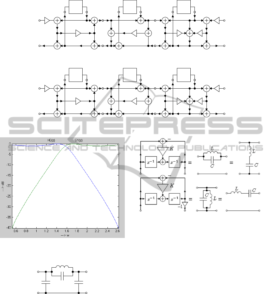
Figure 5: Two channel filter bank.
H(s) =
1
2.035s
3
+ 2.0116s
2
+ 2.5206s + 1.000
=
1
h(s)
(8)
Relevant characteristic function of the transfer
function (8) is
F(s) =
1
2.5206s
3
+ 1.5265s
=
1
f (s)
(9)
From these relations input impedance Z
e
(s) of the
circuit can be obtained in form:
Z
e
(s) =
h(s) + f (s)
h(s) − f (s)
=
4.0707s
3
+ 2.0116s
2
+ 4.072s + 1
2.0116s
2
+ 0.9941s + 1
(10)
We expand Z
e
(s) in continued fraction about zero.
The impedance Z
e
(s) can be constructed using the
Foster preamble techniques (Weinberg, 1962).
Z
e
(s) =
1
2.0235s +
1
0.9941s+
1
2.0235s+1
(11)
DesignofaFilter-bankbytheWaveDigitalFilterTechnique-AnapproachfortheChebishevBank-FilterbytheWave
DigitalFilterTechnique
679

The corresponding LC circuit is shown in figure
6. Discrete realization of the wave digital filter is ob-
tained from this LC prototype of the Chebyshev filter,
see Fig. 8. High-pass filter in the filter-bank synthesis
has the same structure and values as high-pass filter
in the filter-bank analysis, only the multiplier -1 at the
end of each delay elements must be added, see Fig. 9,
(B. Psenicka and Rodriguez, 2006).
0.9941
2.0235 2.0235
Figure 6: LC prototype of Chebyshev low-pass filter.
LC ladder network in Fig.6 can be redrawn net-
work in Fig. 7. The elements are connected with the
parallel and serial adapters together. Parallel depen-
dent adapter have to be used in the end of the struc-
ture.
R
0
R
3
L = 0.9941
C = 2.0235 C = 2.0235
R
1
R
2
Figure 7: LC prototype of Chebyshev low-pass filter – re-
drawn diagram.
To obtain the multiplier coefficients of the discrete
Chebyshev low-pass filter the conductances G
1
and
G
2
must be calculated first.
R
0
= 1 R
3
= 1 (12)
G
1
= G
0
+C = 3.0235 R
1
= 0.33074 (13)
R
2
= R1 + L = 1.32484 G
2
= 0.754806 (14)
Finally the multiplier coefficients of the discrete
low-pass Chebychev filter can be calculated by fol-
lowing relations:
A
1
=
G
0
G
0
+C
= 0.3307 B
2
=
R
1
R
1
+L
= 0.2496
A
31
=
2G
2
G
2
+C+G
3
= 0.3995 A
32
=
2G
3
G
2
+C+G
3
= 0.5293
(15)
Attenuation of the low-pass Chebyshev filter can
be obtained by following script. The script was writ-
ten according the structure in Fig. 8. The attenuation
of the low-pass and high-pass filter are presented in
the Fig. 10. Attenuation of the high-pass filter can
be obtained by changing the signs of variables in the
script: N2 = −N1, N4 = −N3 and N6 = −N5.
A1=0.3307; B2=0.2496; A31=0.3995; A32=0.5293;
N2=0; N4=0; N6=0; XN=1;
for i=1:1:200
XN1=N2-N2*A1+XN*A1;
XN2=XN1+N4;
BN2=XN2-A31*XN2+2*N6-N6*A31-N6*A32;
BN1=XN1-B2*XN2-B2*BN2;
N1=XN*A1-A1*N2+BN1;
N3=BN1+BN2;
N5=N6-XN2*A31-N6*A31-N6*A32;
YN(i)=2*N6-N6*A31-N6*A32-XN2*A31;
N2=N1; N4=N3; N6=N5; XN=0;
end
[h,w]=freqz(YN,1,50)
plot(w,20*log10(abs(h)))
axis([0.5184 2.623-40.3 0])
Minimum attenuation of the high-pass Inverse
Chebyshev filter in the analysis part of filter-bank
must be calculated from the ripple factor of the low-
pass filter in the analysis part of the filter-bank by re-
lation (16), (Weinberg, 1962).
A
min
= 10log
10
(
1
10
A
max
10
−1
+ 1) (16)
Transfer function of inverse Chebyshev filter in s
domain is then given by:
H(s) =
s
2
+ 1.3333
0.655s
3
+ 1.6512s
2
+ 1.3177s + 1.3333
=
k(s)
h(s)
(17)
Relevant characteristic function to the relation
(17) is
F(s) =
s
2
+ 1.3333
0.6550s
2
=
k(s)
f (s)
(18)
Input impedance z
11
and transfer impedance z
12
can be calculated from equation (17) and (18). Inverse
Chebyshev low-pass filter presented in Fig. 11 can
be obtained from these impedances (z
11
, z
12
), (Storer,
1957).
Discrete realization of the parallel LC circuit from
Fig. 11 is demonstrated in the Fig. 12, where K is
given by equation (19), (Kammeyer and K, 1992).
K =
1 − LC
1 + LC
(19)
The coefficients of the serial and parallel adapters
of the discrete filter in figure 18 obtained by equation
(5) are A
1
= 0.6693, B
2
= 0.2496, A
31
= 0.7032 A
32
=
0.5293 and K = 0.1428. Discrete Chebychev high-
pass filter is obtained from the discrete low-pass filter
by changing the sings as is seen in Fig. 19.
Attenuation of the Inverse Chebyshev filter can be
calculated by the following Matlab script. The script
is written according the structure in Fig. 18.
ICINCO2014-11thInternationalConferenceonInformaticsinControl,AutomationandRobotics
680
−A
1
N
2
N
1
X
N
−1
X
N1
B
N1
−B
2
N
4
N
3
b
3
a
3
−A
32
N
6
N
5
Y
N1
−A
31
−1
z
−1
z
−1
B
N
z
−1
Figure 8: Discrete low-pass Chebyshev filter in analysis filter-bank.
−A
1
N
2
N
1
X
N
−1
X
N1
B
N1
−B
2
N
4
N
3
b
3
a
3
−A
32
N
6
N
5
Y
N1
−A
31
−1
z
−1
z
−1
− −
−
− −
B
N
z
−1
Figure 9: Discrete high-pass Chebyshev filter in synthesis filter bank.
Figure 10: Attenuations of the low-pass and high-pass
Chebyshev filter.
C
1
C
2
L
2
C
3
Figure 11: LC prototype of the inverse Chebyshev low-pass
filter.
XN=1;A1=0.6693;B2=0.5423;A31=0.7032;A32=0.8678;
N2=0;N4=0;N6=0;N8=0;K1=0.1428;
for i=1:1:200
XN1=N2-N2*A1+XN*A1;
XN2=XN1+N6;
BN2=XN2-XN2*A31-2*N8-N8*A31-N8*A32;
BN1=XN1-BN2*B2-XN2*B2;
N1=XN*A1-N2*A1+BN1;
N3=BN1+BN2;
Figure 12: Realization of the dual LC structures by discrete
structure.
N5=N3*K1+N4-N6*K1;
N7=N8-N8*A31-N8*A32-XN2*A31;
YN(i)=2*N8-N8*A31-N8*A32-XN2*A31;
N2=N1;N4=N3;N6=N5;N8=N7;XN=0;
end
XN=1;K1=-0.1428;
for i=1:1:200
XN1=N2-N2*A1+XN*A1;
XN2=XN1+N6;
BN2=XN2-XN2*A31-2*N8-N8*A31-N8*A32;
BN1=XN1-BN2*B2-XN2*B2;
N1=XN*A1-N2*A1+BN1;
N3=BN1+BN2;
N5=N3*K1+N4-N6*K1;
N7=N8-N8*A31-N8*A32-XN2*A31;
YN1(i)=2*N8-N8*A31-N8*A32-XN2*A31;
N2=-N1;N4=N3;N6=N5;N8=-N7;XN=0;
end
[h,w]=freqz(YN,1,200);
[h1,w]=freqz(YN1,1,200);
plot(w,20*log10(abs(h)),w,20*log10(abs(h1)))
The attenuation of the Chebyshev inverse low-
DesignofaFilter-bankbytheWaveDigitalFilterTechnique-AnapproachfortheChebishevBank-FilterbytheWave
DigitalFilterTechnique
681
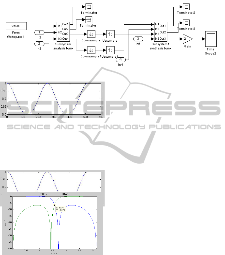
Figure 15: Simulink model of the wave digital filter-bank.
(a)
(b)
Figure 13: Magnitude frequency response of the whole
filter-bank using Chebyshev and Inverse Chebyshev filters
(a), and only Chebyshev filters (b).
Figure 14: Attenuation of the low-pass and high-pass In-
verse Chebyshev filter.
pass and high-pass wave digital filter is presented in
figure 14.
A model of the wave digital filter-bank for
Simulink is in Fig. 15. This model was constructed
from filters in Fig. 8, 9, 18 and 19.
Transfer function T F(z) of the whole filter-bank
can be expressed as
T F(z) = H
0
(z)G
0
(z) + H
1
(z)G
1
(z)
The frequency response of the whole filter-bank
are shown in Fig. 13. Our realization using Cheby-
shev and Inverse Chebyshev filters gives better results
Fig. (a) in comparison with filter-bank using only
Chebyshev filters, Fig. (b). The frequency response
of the whole filter-bank cannot fully meet the condi-
tion for perfect reconstruction T F(z) = 2z
k
. However
the error is small enough for many applications.
The properties of the designed filter-bank was
tested by a speech signal. This signal was applied
to the input of the filter-bank, while the output of the
filter-bank was connected to Simulink oscilloscope.
Input and output signal waveforms of the filter-bank
excited by the speech signal is demonstrated in Fig. 16
and 17. Both input and output signals are near the
same. It is confirmation of the previous result. Our
realization of filter-bank is applicable for speech ap-
plications. Filter-bank composed from Chebyshev
and Inverse Chebyshev filters has better properties
in comparative with the filter-bank constructed only
with low-pass and high-pass Chebyshev filters.
3 CONCLUSIONS
Though the structure of the wave digital filter is more
complicated than other structures, the algorithm for
implementation on the DSP is very simple and it is
very easy to propose general algorithm for arbitrary
order of wave digital filter. These structures are less
sensitive to the quantization error as other types of
filters. Tables of the values A
i
and B
i
of the wave
digital filters can be easily created by small modifi-
cation of the presented design.The parts of the pre-
sented programs can be utilized for implementation of
the Wave Digital Fiter (WDF) in digital signal proces-
sors. Filter-bank from Chebyshev end inverse Cheby-
shev filters was designed in this article and simulated
ICINCO2014-11thInternationalConferenceonInformaticsinControl,AutomationandRobotics
682
−A
1
N
2
N
1
X
N
−1
X
N1
B
N1
−B
2
N
6
N
3
b
3
a
3
−A
32
N
8
N
7
Y
N
−A
31
−1
z
−1
B
N
K
z
−1
z
−1
N
4
N
5
z
−1
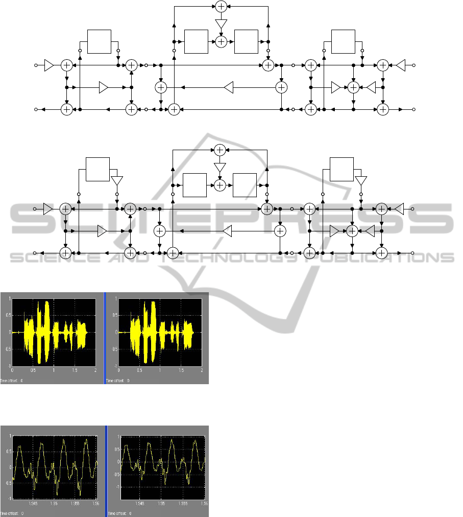
Figure 18: Discrete low-pass inverse Chebyshev filter in analysis filter-bank.
−A
1
N
2
N
1
X
N
−1
X
N1
B
N1
−B
2
N
6
N
3
b
3
a
3
−A
32
N
8
N
7
Y
N
−A
31
−1
z
−1
−
B
N
K
z
−1
z
−1
−
N
4
N
5
−1 −1
z
−1
Figure 19: Discrete high-pass inverse Chebishev filter in synthesis filter-bank.
Figure 16: Input and output signal waveforms of the filter-
bank – whole speech.
Figure 17: Input and output signal waveforms of the filter-
bank – detail.
by signal processing Matlab toolbox containing the
speech signal saved in Workspace.
ACKNOWLEDGEMENTS
The work has been supported by the research project
DGAPA-PAPIIT IN-114012 of the National Au-
tonomous University of Mexico
REFERENCES
B. Psenicka, F. G. U. and Rodriguez, M. A. (2006). Im-
plementation of the wave digital filters on a dsp using
simulink. IASTED Internacional conference Circuits
Signal and Systems: San Francisco, USA.
Fettweis, A. (1972). Digital filter structures related to clas-
sical filter networks. Arch. Elektron. Uebertragun-
stech.
Fettweis, A. and Meerkotter, K. (1975). On adaptors for
wave digital filters. IEEE Trans. on Acoustics, Speech,
and Signal Processing, vol. ASSP-23.
Kammeyer, K. and K, K. K. (1992). Digitale Signalverar-
beitung, Filterung und Spektralanalyse. Teubner Stu-
dienb
¨
ucher.
Keiser, U. (1985). Wave digital filters and their significance
for customized digital signal processing. TI Engineer-
ing Journal-Engeneering Technology.
Mitra, S. K. (1998). Digital Signal Processing, A Computer
bassed approach. McGRAW HILL.
Sedlmeyer, A. and Fettweis, A. (1973). Digital filters with
true ladder configurations. Int. J. Circuit Theory and
Appl.
Storer, J. E. (1957). Passive Network Synthesis. McGRAW
HILL.
Weinberg, L. (1962). Network Analysis and Synthesis. Mc-
GRAW HILL.
DesignofaFilter-bankbytheWaveDigitalFilterTechnique-AnapproachfortheChebishevBank-FilterbytheWave
DigitalFilterTechnique
683
