
Molecular Beam Epitaxy of (Er
x
Sc
1-x
)
2
O
3
on Si(111)
for Active Integrated Optical Devices
H. Omi
1,2
, T. Tawara
1,2
, T. Hozumi
3
, R. Kaji
3
, S. Adachi
3
, H. Gotoh
1
and T. Sogawa
1
1
NTT Basic Research Laboratories, NTT Corporation, Atsugi-shi, Japan
2
NTT Nanophotonics Center, NTT Corporation, Atsugi-shi, Japan
3
Hokkaido University, Sapporo, Japan
Keywords: Er, Sc
2
O
3
, Si, Molecular Beam Epitaxy.
Abstract: We grew (Er
x
Sc
1-x
)
2
O
3
films on Si(111) as a function of x using the molecular beam epitaxy method. The
films were characterized by synchrotron grazing incidence and normal X-ray diffraction, cross-sectional
transmission electron microscopy, and photoluminescence measurements in spectrum and time domains.
We succeeded in obtaining (Er
x
Sc
1-x
)
2
O
3
films on Si(111) that are strained and exhibit 1.5-m light
emission from Er
3+
ions at 4 K and room temperature. We found that the epitaxial Er-doped Sc
2
O
3
films are
better candidates as a light emitting material than epitaxial layers of Er
2
O
3
on Si(111).
1 INTRODUCTION
Integration of cubic (bixbyite-type) sesquioxides on
a Si platform has high potential to improve the
performance of Si circuits by incorporating new
functionalities as alternative gate oxides and light
emitting materials (Grivas, 2008, Reiner, 2010,
Bradley, 2011, Michael, 2009). Among the oxides,
Sc
2
O
3
is one of the most promising as a host material
of rare-earth ions-doped light emitters on Si
substrates (Grivas, 2008, Ter-Gabrielyan, 2011,
Merkle, 2013). The thermal conductivity of Sc
2
O
3
is
the largest among the bixbyite-type oxides,
including Y
2
O
3
and rare earth oxides, and larger than
that of yttrium aluminium garnet (YAG) crystal. The
high thermal conductivity could enable us to obtain
high-power light emission on Si. In fact, recent
researches have shown that Er-doped Sc
2
O
3
ceramics exhibit lasing at the wavelength of 1.58 m
with high quantum efficiency at low temperatures
(Gheorghe, 2008, Kühn, 2009, Ter-Gabrielyan, 2011,
Merkle, 2013). However, to the best of our
knowledge, growth of Er-doped Sc
2
O
3
has not been
achieved on Si, even though Er ions have been
successfully doped in Sc
2
O
3
single and nano-crystals
(Krsmanovic, 2006, Gün, 2007) and the energy
levels of Er
3+
in Sc
2
O
3
ceramics are well-established
(Trabelsi, 2010). This is mainly due to the large
lattice misfit between Sc
2
O
3
and Si. The misfit
between lattice constant of Sc
2
O
3
and two times that
of Si is about 9%. Fortunately, despite the large
misfit, high-quality Sc
2
O
3
films with misfit
dislocations have been grown on a miscut Si(111) as
well as in the system of Gd
2
O
3
on Si(111) by using
the molecular beam epitaxy (MBE) method (Klenov,
2005, Hong, 2005, Chen, 2005). The defects,
including such interfacial dislocations, however,
should be avoided as much as possible for optical
applications.
In this work, we grew epitaxial Er-doped Sc
2
O
3
films on Si(111) using MBE as a function of Er
concentration and characterized the structural and
optical properties of the epitaxial films by
synchrotron grazing incidence X-ray diffraction
(GIXD), X-ray diffraction (XRD), cross-sectional
transmission electron microscope (XTEM), and
photoluminescence (PL) measurements. We will
show that high-quality Er-doped epitaxial Sc
2
O
3
films that exhibit 1.5-m light emission from Er
3+
ions can be grown on Si(111) by using MBE.
2 EXPERIMENTS
The heteroepitaxial growths of Er-doped Sc
2
O
3
were
performed on Si(111) substrates in an MBE chamber
equipped with reflection high-energy diffraction
(RHEED) apparatus. Sc
2
O
3
and Er
2
O
3
were
175
Omi H., Tawara T., Hozumi T., Kaji R., Adachi S., Gotoh H. and Sogawa T..
Molecular Beam Epitaxy of (ErxSc1-x)2O3 on Si(111) for Active Integrated Optical Devices.
DOI: 10.5220/0004762001750179
In Proceedings of 2nd International Conference on Photonics, Optics and Laser Technology (PHOTOPTICS-2014), pages 175-179
ISBN: 978-989-758-008-6
Copyright
c
2014 SCITEPRESS (Science and Technology Publications, Lda.)
simultaneously deposited by electron beam
depositions. The films were grown at the substrate
temperature of 400 - 700℃. Before the depositions,
a (7 × 7) structure was obtained on Si(111).
Reflection high energy diffraction was used to
monitor structures during the growth. Synchrotron
GIXD experiments were performed at beamline
BL15 in SPring-8. The incident X-ray energy was 15
keV. XRD measurements were also carried out in
the single-crystal geometry using an X-ray
diffraction diffractometer (X’pert-Pro MRD; Philips
co.) with Cu K
radiation. XTEM/X-ray energy
dispersive spectroscopy (EDS) images were
obtained at 300/200 kV. PL measurements were
performed using a Raman/PL system (Renishaw,
Model inVia Reflex/StreamLine). PL spectra were
obtained at room temperature using a cooled InGaAs
detector (Princeton Instruments, Model OMA-
V:2.2). PL measurements at low temperatures were
performed in another PL system (Omi, 2012, Tawara,
2013).
3 RESULTS AND DISCUSSION
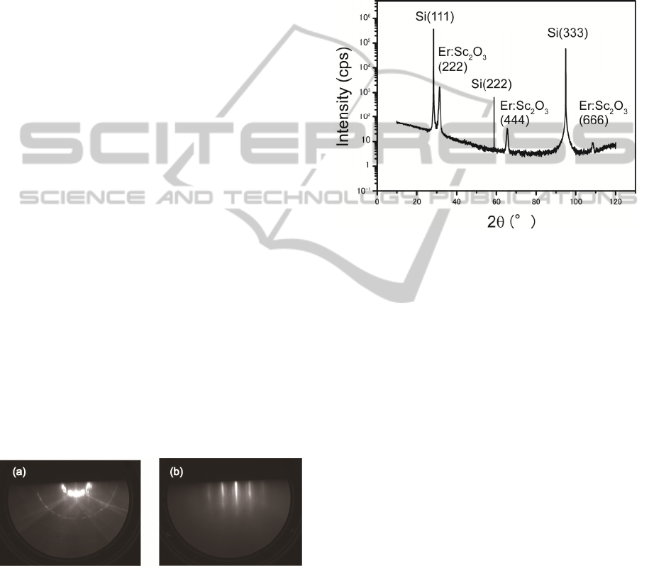
Figure 1 shows the RHEED patterns obtained from
the Si(111)-(7×7) surface and during the growth of
(Er
x
Sc
1-x
)
2
O
3
film on the Si(111)-(7×7) surface at
700℃. The RHEED pattern exhibits sharp streaks
with a (4×4) structure, indicating that the epitaxial
film grows two dimensionally on the Si(111)
substrate. The formation of the (4×4) structure on
the surface is in good accordance with the formation
of Sc
2
O
3
and Gd
2
O
3
epitaxial layers on Si(111)
(Trabelsi, 2010, Klenov, 2005, Hong, 2005, Wang,
2009).
Figure 1: (a) (7 × 7) RHEED pattern from Si (111)
substrate. (b) (4×4) RHEED pattern during (Er
x
Sc
1-x
)
2
O
3
(x = 0.03) growth on Si(111). Electron beams are parallel
to the <110> direction.
Figure 2 shows the scan XRD profile
obtained from a 21-nm-thick (Er
x
Sc
1-x
)
2
O
3
film
grown on Si(111). The peaks at 31.395 degrees
is from the (222) reflections from the film. The
relationship between the film and substrate is [111]
(Er
x
Sc
1-x
)
2
O
3
//[111]Si. The lattice constant of the
(222) plane is characterized to be 2.847 Å, which is
between 2.843 Å for Sc
2
O
3
and 3.045Å for Er
2
O
3
.
The out-of-plane experiment shows that the lattice
constant of the (Er
x
Sc
1-x
)
2
O
3
film is almost equal to
the lattice constant of Sc
2
O
3
. Additional scan
experiments show that the film exhibits single
domain on Si(111).
Figure 2: scan XRD profile obtained from the 21-
nm-thick (Er
x
Sc
1-x
)
2
O
3
(x = 0.03) film grown on Si(111).
Figure 3 shows the GIXD profile from the
(Er
x
Sc
1-x
)
2
O
3
film grown on Si(111). As seen in this
figure, three peaks are evident in addition to the
sharp peak from the Si(220). This suggests that the
epitaxial film/Si(111) stacks have cube-on-cube
structures with orientation relationships [111]
(Er
x
Sc
1-x
)
2
O
3
//[111]Si and [1-10] (Er
x
Sc
1-x
)
2
O
3
//[-
110]Si, which are consistent with those observed in
the Sc
2
O
3
/Si(111) stacks (Chen, 2005). The main
peak is from (440) reflection from the film, which is
at 12.452 degrees. From the peak position, the
lattice constant of (440) is estimated to be 1.917Å,
which almost matches the 1.92Å of Si(-220) planes,
indicating that the epitaxial (Er
x
Sc
1-x
)
2
O
3
films are
significantly strained in-plane and that the lattice
mismatch between Si and (Er
x
Sc
1-x
)
2
O
3
film is not
relieved by a hexagonal misfit dislocation networks,
which were observed in the Sc
2
O
3
/Si(111) system by
Klenov et al. (Klenov, 2005). Note here that the
lattice constant of (440) planes are 1.74 and 1.865 Å
for Sc
2
O
3
and Er
2
O
3
, respectively. The peaks at
12.071 and 13.008 degrees are from silicides
formed at the interface between the film and
substrate (See Fig. 4).
PHOTOPTICS2014-InternationalConferenceonPhotonics,OpticsandLaserTechnology
176
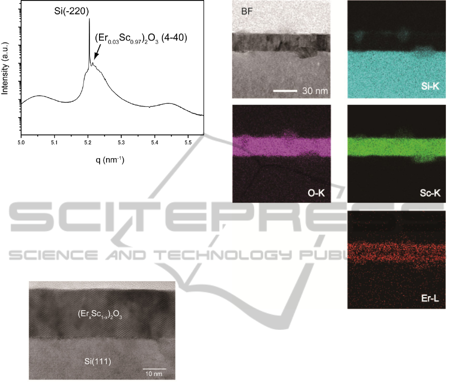
Figure 3: In-plane GIXD line scan around the
(Er
0.03
Sc
0.97
)
2
O
3
(4-40) peak along [-110]Si.
Figure 4 shows an XTEM image obtained from
the 21-nm-thick (Er
x
Sc
1-x
)
2
O
3
film grown on Si(111).
As seen in this image, we could not find significant
defects in the film and oxide layers at the interface,
indicating that we obtained high-quality epitaxial
(Er
x
Sc
1-x
)
2
O
3
layers on Si(111).
Figure 4: XTEM image of (Er
0.03
Sc
0.97
)
2
O
3
/Si(111).
Figure 5 shows an XTEM image and
corresponding EDS images obtained from the
(Er
x
Sc
1-x
)
2
O
3
film grown on Si(111). The images
clearly show that the (Er
x
Sc
1-x
)
2
O
3
film coherently
grows on Si(111). From the EDS mapping, we can
see that the Er atoms are actually incorporated into
the whole film and the Er concentration is estimated
to be 1 at%. The Er concentration in the film was
also confirmed to be 1.2 at% by an additional
Rutherford back-scattering experiment. In addition,
a nanoscale particle can be seen at the interface.
Electron diffraction from the particle and EDS
images show that the particle has the Sc
3
Si
5
structure,
which is in good agreement with the GIXD results in
Fig 3.
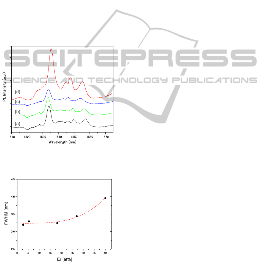
Figure 6 shows the PL spectrum obtained at
room temperature from the (Er
x
Sc
1-x
)
2
O
3
films
grown on Si(111) with pumping at 532 nm. The
Figure 5: Bright field XTEM image (BF) and
corresponding EDS images for Si, O, Sc, and Er.
films show PL emission at 1533 nm from Er
3+
ions
in the (Er
x
Sc
1-x
)
2
O
3
films at x= 0.068, 0.134, and
0.676 and emission at 1535 nm in the Er
2
O
3
. The
emissions are due to the transition between the
energy levels (
4
I
15/2
-
4
I
13/2
). The difference in the
main peak positions indicates that the crystal fields
around Er
3+
ions in the (Er
x
Sc
1-x
)
2
O
3
and Er
2
O
3
are
not identical. The peaks are observed to become
broader with an increase of x, as seen in Fig. 7. We
also obtained PL spectra from the films at 4 K with
pumping at 1535 nm. The PL spectra have peaks at
1551 nm, which are originated from the transition
between energy levels Y’
1
and Z’
1
of Er
3+
ions
located at C
3i
sites of the (Er
x
Sc
1-x
)
2
O
3
films with x =
0.068, 0.134, and 0.676 (Tawara, to be published).
The peaks become sharper and their lifetime become
longer (from the order of microseconds to
milliseconds) than those of the epitaxial Er
2
O
3
film
grown on Si(111) by MBE at 4 K (Tawara, 2013).
For example, the lifetime of the 1.551-m
emission from Er
3+
ions in the (Er
0.068
Sc
0.932
)
2
O
3
film
was observed to be 2.2 ms at 4 K. The lifetime is
compatible to those of (Er
x
Yb
1-x
)
2
SiO
5
and (Er
x
Y
1-
x
)
2
SiO
5
polycrystalline films grown on Si substrates
MolecularBeamEpitaxyof(ErxSc1-x)2O3onSi(111)forActiveIntegratedOpticalDevices
177
when x is about 0.136 (Yin, 2012), indicating that
the epitaxial layers have good potential as a optical-
gain material.
Note that the interfacial silicides shown in Figs.
2 and 5 are optically inactive (Adler, 1992).
Finally, we discuss the quantum efficiency of
Er
3+
emission from the epitaxial (Er
x
Sc
1-x
)
2
O
3
films
on Si(111). For the films, the decay time of Er
3+
emission is 150 s at x = 1 (Tawara, 2013) and 2.2
ms at x = 0.068 (Tawara, to be submitted). The
radiative life time
r
of Er
3+
in Y
2
O
3
(Thiel, 2011)
and SiO
2
(Lawrence 2013) are 14.6 and 20 ms,
respectively. Therefore, quantum efficiency
r
is
roughly estimated to be 1 % at x = 1 and on the
order of 10 % at x = 0.068. We believe, however,
that the quantum efficiency will become larger when
Figure 6: PL spectra obtained from the (Er
x
Sc
1-x
)
2
O
3
films
grown on Si(111) at room temperature with pumping at
532 nm. (a) x = 0.068, (b) x = 0.134, (c) x = 0.676, and (d)
x = 1.
Figure 7: Plots of full width at half maximum (FWHM) of
main peaks in Fig. 6 as a function of Er concentration in
the epitaxial films. The FWHM of the main peaks are
derived by fitting with Gaussian function. The dotted line
is a guide for eye.
x is optimized, as was observed in the
polycrystalline (Er
x
Y
1-x
)
2
O
3
films on Si(100) (Savio,
2009). Lifetime measurements of the epitaxial film
as a function of x are in progress.
4 CONCLUSIONS
We succeeded in obtaining (Er
x
Sc
1-x
)
2
O
3
epitaxial
layers on Si(111) using the molecular beam epitaxy
method with x from 0.068 to 1, even though they
have large misfit between them. The as-grown film
has a cubic bixbyite structure with three-fold
symmetry. The films grew on Si(111) substrate with
orientation relationships [111] (Er
x
Sc
1-x
)
2
O
3
//[111]Si
and [1-10] (Er
x
Sc
1-x
)
2
O
3
//[-110]Si. The film at x =
0.068 is strained along the in-plane direction but not
along the out-of-plane direction. The (Er
x
Sc
1-x
)
2
O
3
films with x = 0.068, 0.134, and 0.676 exhibit PL
luminescence at 1.5-m at room temperature with
pumping at 532 nm. The 1.551-m luminescence
becomes sharper and its lifetime becomes longer
than those of Er
2
O
3
epitaxial films on Si(111) at 4 K
with pumping at 1535 nm. The Er-doped epitaxial
Sc
2
O
3
films have potential as an optical-gain
material on the Si platform.
ACKNOWLEDGEMENTS
We thank Drs. Shingo Takeda and Kazushi
Yokoyama for his help in the synchrotron radiation
experiments at beamline BL15 in SPring-8. We also
thank Prof. H. Isshiki and Dr. T. Nakajima for useful
discussion. This work was partially supported by
JSPS KAKENHI Grant Number 24360033.
REFERENCES
Adler D. L., Jacobson D. C., Eaglesham D. J., Marcus M.
A., Benton J. L., Poate J. M., and Citrin P. H., 1992.
Appl. Phys. Lett. 61, 2181.
Bradley J. D. B. and Pollnau, M. 2011. Laser Photonics.
Rev. 5, 368.
Chen C. P., Hong M., Kwo J., Cheng H. M., Huang Y. L.,
Lin S. Y., Chi J., Lee H. Y., Hsieh Y. F., and
Mannaerts J. P., 2005. J. Crystal Growth 278, 638.
Gheorghe C., Georgescu S., Lupei V., Lupei A., and
Ikesue A., 2008. J. Appl. Phys. 103, 083116.
Gün T., Kuzminykh Y., Petermann K., Scheife H., and
Huber G. 2007. Appl. Phys. Lett. 91, 083103.
Grivas C. and Eason R. W., 2008. J. Phys.: Condens.
Matter. 20, 264011.
PHOTOPTICS2014-InternationalConferenceonPhotonics,OpticsandLaserTechnology
178

Hong M., Kortan A. R., Chang P., Huang Y. L., Chen C.
P., and Chou H. Y., 2005. Appl. Phys. Lett. 87, 251902.
Klenov D. O., Edge L. F., Schlom D. G., and Stemmer S.,
2005. Appl. Phys. Lett. 86, 051901.
Kühn H., Fechner M., Kahn A., Scheife H., and Huber G.,
2009, Opt. Mater. 31, 1636.
Krsmanovic R., Lebedev O. I., Speghini A., Bettinelli M.,
Polizzi S., and Tendeloo G. V., 2006. Nanotechnology
17, 2805.
Lawrence N., Negro L. D., 2013. Nano Lett. 13, 3709.
Merkle L. D., Ter-Gabrielyan N., 2013. Proc. SPIE 8733,
87330H-8.
Michael C. P., Sabnis V. A., Yuen H. B., Jamora A.,
Semans S., Atanackovic P. B., and Painter O., 2009.
Appl. Phys. Lett. 94, 131103.
Omi H. and Tawara T., 2012. Jpn. J. Appl. Phys. 51,
02BG07.
Reiner J. W., Kolpak A. M., Segal Y., Carrity K. F.,
Ismail-Beigi S., Ahn C. H., and Walker F., 2010. Adv.
Mater. 22, 2919.
Savio R. L., Miritello M., Cardile P., Priolo F., 2009. J.
Appl. Phys. 106, 043512.
Tawara T., Omi H., Hozumi T., Kaji R., Adachi S., Gotoh
H., and Sogawa T., 2013. Appl. Phys. Lett. 102,
241918.
Tawara T., Omi H., Hozumi T., Kaji R., Adachi S., Gotoh
H., and Sogawa T., to be published.
Ter-Gabrielyan N., Fromzel V., and Dubinskii M., 2011.
Opt. Mat. Expr. 1, 503.
Thiel C. W., Böttger T., Cone R. L., 2011. J. Lumin. 131,
353.
Trabelsi I., Maalej R., Dammak M., Lupei A., and
Kamoun M., 2010. J. Lumin., 130, 927.
Wang J. X., Laha A., Fissel A., Schwendt D., Dargis R.,
Watahiki T., Shayduk R., Braun W., Liu T. M., and
Osten H. J., 2009. Semicond. Sci. Technol. 24, 045021.
Yin L., Ning H., Turkdogan S., Liu Z., Nichols P., and
Ning C. Z., 2012. Appl. Phys. Lett. 100, 241905.
MolecularBeamEpitaxyof(ErxSc1-x)2O3onSi(111)forActiveIntegratedOpticalDevices
179
