
High Density Cell Electrofusion on Chip using an Array of
Non-connected Metallic Pads
Feriel Hamdi
1,3
, Wei Wang
1
, Frederic Subra
2
, Elisabeth Dufour-Gergam
3
, Olivier Francais
1
and Bruno Le Pioufle
1
1
Ecole Normale Supérieure de Cachan, CNRS, SATIE, UMR 8029, Cachan, France
2
Ecole Normale Supérieure de Cachan, CNRS, LBPA, UMR 8113, Cachan, France
3
Univ Paris-Sud, CNRS, Institut d’Electronique Fondamentale, UMR 8622, Orsay, France
Keywords: Electrofusion, Dielectrophoresis, High Density, Microfluidics.
Abstract: Cell fusion consists on creating a hybridoma cell containing the genetic properties of the progenitor cells. It
can be performed chemically or electrically. The latter method, called Electrofusion, is a more efficient way
to create hybrid cells investigated for antibody production or cancer immunotherapy. To envision this
application, a high amount of hybrid cells is needed. This work presents an original design for high density
electrofusion on chip. The structure consists of an array of non-connected electroplated gold pads patterned
between two connected electrodes. While applying a Voltage on the connected electrodes, the Electric field
is disturbed around the gold pads inducing a Dielectrophoretic Force on cells used to trap and pair them.
When cells are paired, Electric pulses are applied to induce electrofusion. The absence of wire connections
on the pads permits the high density trapping and electrofusion. Successful alignment and electrofusion of
murine melanoma cells with this structure are demonstrated.
1 INTRODUCTION
Cell fusion is a method to generate a hybrid cell
which combines specific properties of its progenitor
cells. While cell fusion has been developed for
antibody production (Köhler and Milstein, 1975), it
is now also investigated for cancer immunotherapy
(Sukhorukov et al., 2006) and reprogramming of
somatic cells (Tada et al., 2001). There are different
methods for cell fusion, such as biological (Okada,
1958), chemical (Pontecorvo, 1975) and electric
pulse mediations (electrofusion). For electrofusion,
the operation is simple and the system is free of
chemical or genetic contaminations. Combined to
the high fusion efficiency (Skelley et al., 2009)), this
makes the method widely used. Therefore, the most
used method for electrofusion consists on using an
electroporation cuvette composed of two facing
electrodes with 1 to 4 mm distance or ellipsoidal
ones with 200µm inter-electrodes distance
(Eppendorf). In these cuvettes, there is no possible
placing of cells and the yield of one-to-one fusion
cells is very low (20% fusion rate including multiple
cell fusion (Zimmermann et al., 2006)). The use of
small biodevices is investigated since 1989 (Masuda
et al., 1989) to solve this problem by a primary step
of placing cells. Different strategies for cell trapping
and pairing were presented such as fluidic (Skelley
et al., 2009) or electric using a Dielectrophoretic
force (Masuda et al. 1989); (Techaumnat et al.,
2008); (Kirschbaum et al., 2012).
Another issue in the development of biodevices
for electrofusion is the yield. Indeed, a large amount
of hybridomas is needed to make an injection, but in
the classic microfabricated structures, the density is
limited because of the electric connections.
In this work, we present a novel structure
dedicated to electrofusion on chip with high density
capability. The structure involves an array of non-
connected micro-size electroplated gold pads,
positioned between two electrodes, which induce a
specific electric field topology. The absence of
wiring, and connections, as gold structures are not
powered, permits the high density arraying which is
necessary when the high throughput is envisioned
for the electrofusion. The successful self-alignment
of cells in this array, thanks to DiElectroPhoretic
(DEP) forces, followed by the application of
electrofusion pulses is demonstrated.
In this paper, we first introduce the structure
design with an FEM simulation of the electric field.
68
Hamdi F., Wang W., Subra F., Dufour-Gergam E., Français O. and Le Pioufle B..
High Density Cell Electrofusion on Chip using an Array of Non-connected Metallic Pads.
DOI: 10.5220/0004246100680072
In Proceedings of the International Conference on Biomedical Electronics and Devices (BIODEVICES-2013), pages 68-72
ISBN: 978-989-8565-34-1
Copyright
c
2013 SCITEPRESS (Science and Technology Publications, Lda.)
Secondly, the fabrication process of the biochip and
the preparation of cells are presented. Finally,
experiments for cell trapping and electrofusion are
described in the last sections.
2 MATERIALS AND METHODS
In this work, electrofusion on chip is based on the
use of non connected high conductive materials
(gold) to modify the electric field topology between
two electrodes (Figure 1). This enables cells
alignment and pairing between arrayed gold
structures with assistance of DEP force, which is
necessary before initiating the cell electrofusion
protocol. To create the new design, a 3D simulation
of the Electric Field and DEP in the structure had
been achieved using a finite element method
(AC/DC module of COMSOL Multiphysics ©). The
result (figures 2 and 3) shows that with the
appropriate conditions, cells are attracted to the area
between the facing pads.
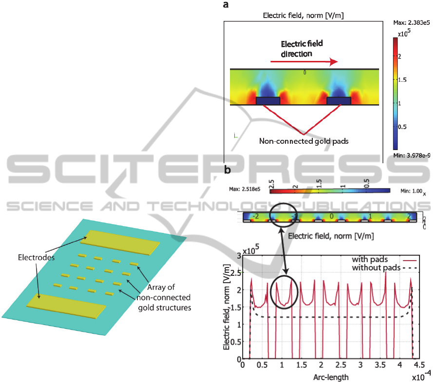
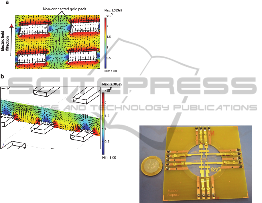
Figure 1: Schematic view of the chip developed showing
electrodes generating electric field and gold structures for
DEP effect.
2.1 Structure Modeling
Using the AC/DC module of COMSOL
Multiphysics, we simulated a structure composed of
an array of 6x4 non-connected metallic pads (10 µm
x 40 µm size separated by 50 µm distance) between
two electrodes (410 µm distance). The metal is 5.5
µm thick gold. The structure was immersed in 25
µm height low conductivity medium (0.03 S/m) and
we applied 50 V on the connected electrodes.
As shown in figure 2a and 2b, the maximum
electric field (E) values are between the gold pads
(parallel to E) close to the edges, while the minima
are above the pads, in the middle and on the edges
perpendicular to the electric field (Figure 3a).
The electric field gradient obtained is used to
trap cells. The gap between pads will then constitute
the fusion zone. Thus, this gap is calculated to be
equivalent to the size of two cells.
Figure 2: a.) Cut view of the 3D simulated structure
showing electric field topology (color) b.) Electric field
distribution along a raw of pads (continuous curve) and
without pads (discontinuous curve)
Figure 2b shows that without the presence of the
non-connected pads, the area between the electrodes
presents a very homogeneous E but lowered to 1.2
kV/cm. If we apply the same voltage with the
presence of the pads, the electric field in the fusion
zone is increased to 1.5 kV/cm.
Due to the non-homogeneity of the electric field
induced by the presence of the pads, insulating
particles (as cells) would experience
Dielectrophoresis in this structure. If we want to trap
cells in the fusion zones, we can apply a sinusoidal
HighDensityCellElectrofusiononChipusinganArrayofNon-connectedMetallicPads
69
wave at a frequency inducing positive
Dielectrophoresis (particles attracted by high E
areas). Indeed, as shown by arrows in figure 3, if
cells are in low E field areas, they will be pushed to
the fusion zone (high E).
Figure 3: 3D simulated structure showing electric field
topology (color) and DEP direction (arrow, case positive).
Therefore, the non-connected pads contribute to:
- increase the electric field in the fusion area
- create a topography of the electric field to induce
cell trapping
In the next section we will present the device
fabrication before introducing the experimental
results obtained with biological cells.
2.2 Biodevice Fabrication
All the materials used for the fabrication of the
device are biocompatible. The chip is fabricated on a
quartz wafer pre-coated with a thin layer of Cr (15
nm Chromium to insure adhesion of Gold) and 150
nm Au as a primer for electroplating. Gold layer
thickness is increased up to 5.5 µm in an electrolytic
bath based on Potassium Aurocyanure KAu[CN]
2
(Dalmay et al., 2011) in order to enhance the electric
field amplitude at the non-connected conductive
pads. A photolithography step (using S1805
pohotresist) followed by a wet etching process (with
KI/I
2
for Gold followed by Cr etchant
MicroChemicals for Chromium) defined the
electrodes (electric field generation) and the non-
connected gold structures (cell positioning). The
photoresist was then removed by acetone.
Finally, microfluidic channels were made of
thick SU8-2025. That epoxy photoresist was spin-
coated (500 rpm/100 rpm.s
-1
/5 s then 3000 rpm/500
rpm.s
-1
/ 30 s), soft baked (3 min at 65°C, 15 min at
95°C and 3 min at 65°C), insulated (160 mJ), post
exposure baked (same 3 steps than the soft bake) and
developed to form 25 µm high channels. To get a
good adhesion of the photoresist, the device was
hard baked during 2 hours at 175°C.
The device is packaged thanks to a simple
microscope glass slide put on the top of the
microchannel. A printed circuit board holder had
been fabricated to ensure the electrical access to the
micro-electrodes used for electric field generation
(cell positioning (DEP) and electrofusion). A view
of the final device electrically connected to the
power supply through a PCB plate is shown in figure
4.
Figure 4: Global view of the fabricated chip on its PCB
holder.
2.3 Biological Experiments
For biological experiments, mouse melanoma cells
B16F10 had been used. They were suspended in a
low conductivity hypotonic fusion buffer (0.1M
Sorbitol, 0.7 mM MgCl
2
, 0.1 mM Calcium Acetate
and 1 mg/ml BSA) and injected in the fluidic
channel. The diameter of B16F10 cells in this buffer
is around 20 µm.
The experiments were led in static conditions.
An array of 10µm*40µm gold structures separated
by 50 µm has been used in order to be compatible
with the size of paired cells.
BIODEVICES2013-InternationalConferenceonBiomedicalElectronicsandDevices
70
2.3.1 Cell Preparation
B16F10 murine melanoma cells are cultured in
Minimum Essential Medium supplemented with
10% Fetal Bovine Serum and 1% PS antibiotics
(Penicilin-Streptomycin). Cultures were maintained
in a 5% CO
2
incubator at 37°C. Before the
experiment, cells were detached with Trypsin and
suspended in the hypotonic fusion buffer (0.1M
Sorbitol, 0.7 mM MgCl
2
, 0.1 mM Calcium Acetate
and 1 mg/ml BSA). The measured conductivity of
the medium is 272 µS/m.
Low conductivity ensures
stronger pDEP and reduces Joule heating. A
preparation of 1 million cells per ml was used for the
experiments. The diameter of B16F10 cells in this
buffer is around 20 µm.
2.3.2 Cell Trapping
With the presence of non-connected conductive
pads, the application of a voltage between the
electrodes produces a non-uniform electric field
(figure 3). When biological cells are exposed to this
field, they experience a dielectrophoretic force
(Fricke, 1924):
F
DEP
2
R
Cell
3
m
e
K
CM
E
2
(1)
where R
Cell
is cell’s radius, E the electric field, K
CM
the Clausius-Mossotti (CM) factor,
e
[K
CM
] its real
part and ε
m
the extracellular medium permittivity.
K
CM
depends on the applied frequency and the
electric parameters of the cell and the medium.
When K
CM
is positive, cells are attracted to
maximum electric field areas, it is positive DEP
(pDEP).
The DEP signal consists of a sine wave. This
force is convenient to move polarisable particles. It
was investigated for carbon nanotubes or other
particles (Krupke et al., 2004), cell sorting and
trapping (Salmanzadeh et al., 2012) or, as in our
case, cell pairing.
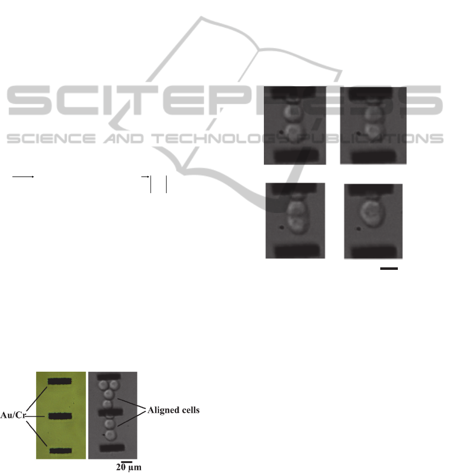
Figure 5: Top view of the non-connected gold pads
arrayed within the microfluidic structure (left) and aligned
cells due to positive DEP force (right).
Experiments describing cell trapping and pairing
are presented in figure 5. A sine wave of 15 Vpp and
400 kHz was used during the experiment to induce
DEP force.
We can see in figure 5 that cells align between
the non-connected pads according to the pDEP
arrows predicted by the simulation shown in figure
3.
2.3.3 Electrofusion
When the cells were paired, electrofusion pulses
were added to DEP signal (10 square pulses of 100
µs duration, equivalent electric field = 1.21 kV/cm).
Successful fusion had been obtained from cells in
the positioning area, between two non connected
gold pads (Figure 6).
Figure 6: Dynamics of cell fusion induced by electric
pulses.
After 12 seconds, the membranes of cells start to
merge to form a hybridoma which regained a
spherical shape 74 seconds after the first pulse.
3 CONCLUSIONS
In this paper we presented a novel structure using
non-connected electroplated gold pads for high
density cell pairing and fusion. The simulation of the
electric field shows the effect of the conductive pads
on the field distribution. Indeed, the presence of the
pads increases the electric field in the fusion areas
without increasing the applied voltage. On the other
hand, due to the non-homogeneity of the electric
field, these pads permit the use of Dielectrophoresis
t=0s t=12.9s
t=18s
t=74.4s
20µm
pads
HighDensityCellElectrofusiononChipusinganArrayofNon-connectedMetallicPads
71

to trap cells prior to electrofusion. We demonstrated
the successful pairing and electrofusion between the
non-connected pads with biological cells. Thanks to
the absence of wiring, this method is a promising
technique for high density cell electrofusion on chip.
ACKNOWLEDGEMENTS
This work was performed thanks to the financial
support of PRES Universud, CNANO’Ile de France,
the ANR PNANO Nanopulsbiochip and the Labex
LASIPS, IMPcell project
REFERENCES
Köhler G. and Milstein C., 1975. Continuous cultures of
fused cells secreting antibody of predefined
specificity, In Nature, 256, 495.
Sukhorukov V. L., Reuss R., Endter J. M., Fehrmann S.,
Katsen-Globa A., Gessner P., Steinbach A., Müller K.
J., Karpas A., Zimmermann U. and Zimmermann H.,
2006. A biophysical approach to the optimisation of
dendritic-tumour cell electrofusion. In Biochemical
and Biophysical Research Communication, 346, 829.
Tada M., Takahama Y., Abe K., Nakatsuji N. and Tada T.,
2001. Nuclear reprogramming of somatic cells by in
vitro hybridization with ES cells. In Current Biology,
11, 1553.
Okada Y., 1958. The fusion of Ehrlich's tumor cells
caused by HVJ virus in vitro. In Biken Journal, 1, 103.
Pontecorvo G., 1975. Production of mammalian somatic
cell hybrids by means of polyethylene glycol
treatment. In Somatic Cell and Molecular Genetics, 1,
397.
Skelley A. M., Kirak O., Suh H., Jaenisch R. and Voldman
J., 2009. Microfluidic control of cell pairing and
fusion. In Nature Methods, 6, 147.
Zimmermann D., Terpitz
U., Zhou A., Reuss R., Müller
K., Sukhorukov V. L.,Gebner P., Nagel G.,
Zimmermann U. and Bamberg E., 2006. Biophysical
characterisation of electrofused giant HEK293-cells as
a novel electrophysiological expression system. In
Biochemical and Biophysical Research
Communications, 348 (2), 673.
Masuda S., Washizu M. and Nanba T., 1989. Novel
method of cell fusion in field constriction area in fluid
integrated circuit. In IEEE Trans. Ind. Appl, 25, 732,
1989
Techaumnat B., Tsuda K., Kurosawa O., Murat G., Oana
H. and Washizu M., 2008. High-yield electrofusion of
biological cells based on field tailoring by
microfabricated structures. In IET Nanobiotechnology,
2 (4), 93.
Kirschbaum M., Guernth-Marschner C. R., Cherré S., Pna
A., Jaeger M. S., Kroczek R. A., Schnelle T., Mueller
T. and Dusch C., 2012. Highly controlled
electrofusion of individually selected cells in
dielectrophoretic field cages. In Lab Chip, 12, 443
Dalmay C., Villemejane J., Joubert V, Francais O., Mir L.
M., Le Pioufle B., 2011. Design and realization of a
microfluidic device devoted to the application of ultra-
short pulses of electrical field to living cells. In
Sensors and Actuators B : Chemical, 160 (1),
1573Fricke H., 1924. J. of Applied Physics, 24, 575
Krupke R., Hennrich F., Kappes M. M. and Löhneysen
H., 2004. Surface Conductance Induced
Dielectrophoresis of Semiconducting Single-Walled
Carbon Nanotubes. In Nano Letters, 4 (8), 1395.
Salmanzadeh A., Kittu H., SSano M. B., Roberts P. C.,
Schmelz E. M., 2012. Dielectrophoretic differentiation
of mouse ovarian surface epithelial cells,
macrophages, and fibroblasts using contactless
dielectrophoresis. In Biomicrofluidics, 6, 024104.
BIODEVICES2013-InternationalConferenceonBiomedicalElectronicsandDevices
72
