
CHITOSAN FOR MEMS
Demonstration of Micromechanical and Optical Biosensors
Stephan T. Koev, Peter H. Dykstra, Reza Ghodssi
MEMS Sensors and Actuators Lab, Institute for Systems Research, Departement of Electrical and Computer Engineering
University of Maryland, College Park, MD 20742, U.S.A.
Gary W. Rubloff
Institute for Systems Research, Department of Materials Science and Engineering
Univerisity of Maryland, College Park, MD 20742, U.S.A.
William E. Bentley
Fischell Department of Bioengineering, Univerisity of Maryland, College Park, MD 20742, U.S.A.
Gregory F. Payne
Center for Biosystems Research, University of Mayland Biotechnology Institute, College Park, MD 20742, U.S.A.
Keywords: Chitosan, MEMS, DNA hybridization, Microcantilever, Fluorescence.
Abstract: This paper presents the biological functionalization of MEMS sensors by using the polysaccharide chitosan.
Chitosan is a unique polymer due to its abundance of primary amine groups and its ability to be
electrodeposited with spatial and temporal control. Biomolecules such as DNA and proteins can be attached
to chitosan films by standard coupling chemistries. This biofunctionalization approach was demonstrated for
two different MEMS devices: a microcantilever and an optical sensor. The devices were coated with
chitosan and probe DNA and were used for detecting the hybridization with target DNA. Here, we describe
the design, fabrication procedure, and testing results for both of these biosensors.
1 INTRODUCTION
Functionalizing surfaces for the detection of specific
analytes is a common practice for many biosensor
devices. Electrochemical sensors, for example, often
employ hydrogels which selectively block the
diffusion of particular molecules or entrap enzymes
to enable specific detection (Geng et al., 2008). It is
a greater challenge to functionalize surfaces of
microelectromechanical systems (MEMS) sensors
due to their small size. MEMS sensors hold many
advantages over their macroscale counterparts,
including low cost due to batch fabrication
techniques, high-throughput screening ability, and
small required sample volumes. Several
functionalization schemes have been demonstrated
for MEMS devices (Mizutani, 2007), including the
self-assembly of thiol labeled molecules to gold
surfaces and of silane labeled molecules to silica
surfaces. These techniques require time consuming
laboratory procedures to ensure the integrity of the
biomolecules and offer limited control over their
patterning.
We report the use of an amine rich
polysaccharide, chitosan, to functionalize surfaces in
both mechanical and optical MEMS biosensors.
Chitosan can be selectively electrodeposited on
patterned conductive surfaces, and it has primary
amine groups at every repeating sugar unit of its
polymer structure (Yi et al., 2005). The amine
groups can be used for covalent attachment of
various biomolecules, making chitosan an excellent
interface between microfabricated devices and
biological components. Here, we present the
attachment of probe DNA to chitosan-coated sensors
used for the detection of target DNA.
109
Koev S., Dykstra P., Ghodssi R., Rubloff G., Bentley W. and Payne G. (2009).
CHITOSAN FOR MEMS - Demonstration of Micromechanical and Optical Biosensors.
In Proceedings of the International Conference on Biomedical Electronics and Devices, pages 109-112
DOI: 10.5220/0001552801090112
Copyright
c
SciTePress
2 CHITOSAN PROPERTIES
Chitosan is derived from the partial deacetylation of
chitin, an abundant material found in nature. At low
pH below a pKa value of 6.3, chitosan is cationic
and soluble in water. However, as the pH rises,
chitosan becomes protonated and insoluble. We take
advantage of chitosan’s pH dependent solubility to
electrodeposit a chitosan film with spatial and
temporal control in the MEMS sensors. In an
electrochemical reaction, the pH at the cathode
surface will rise due to the reduction of the hydrogen
ions. This rise in pH will cause a film of chitosan to
form over the conductive surface with a rate
dependent on the applied bias (Yi et al., 2005).
3 MICROMECHANICAL
SENSOR
3.1 Design
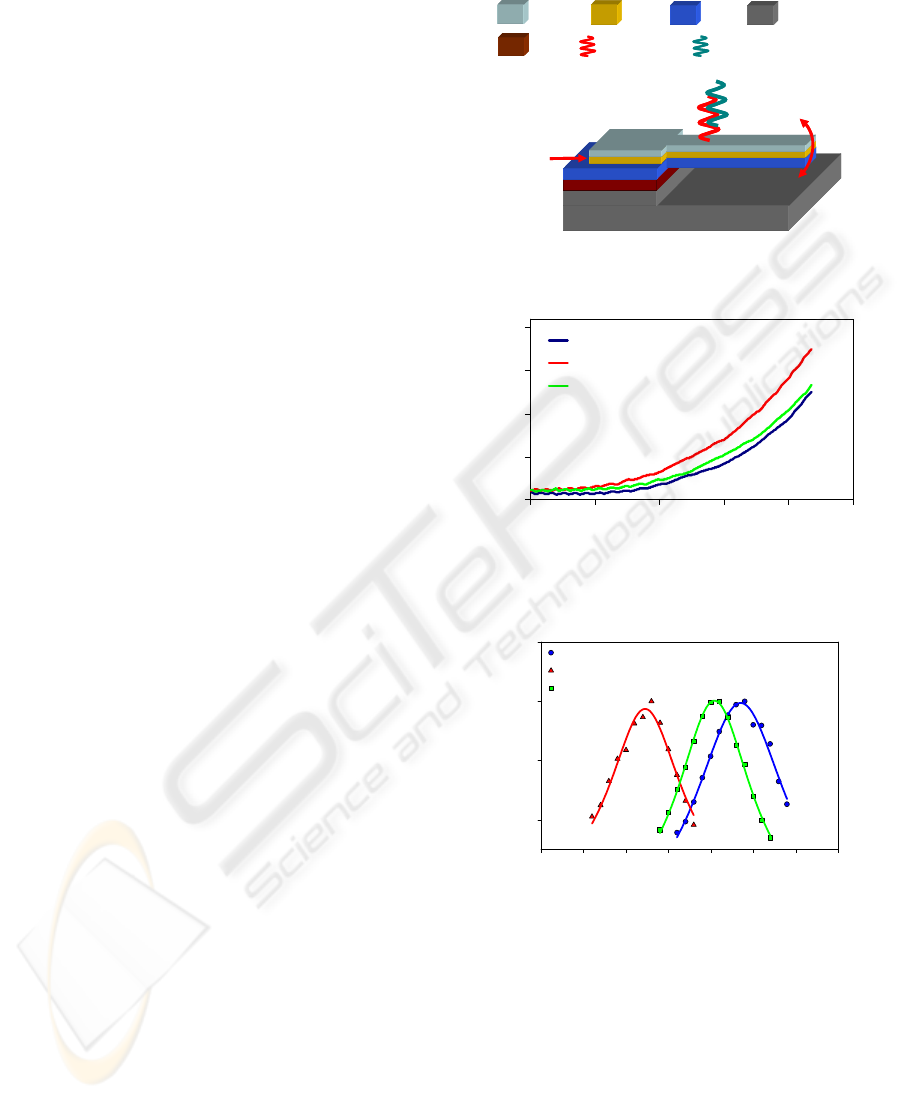
The cantilever sensor consists of layers of Si
3
N
4
(500nm thick), Au/Cr (100nm thick), and chitosan
with probe DNA (~100nm) on a silicon substrate as
shown in Fig. 1 (Koev et al., 2007). The cantilever
length and width are 100μm and 40μm respectively.
When exposed to target DNA with a complementary
sequence to the probe, the target binds to the probe
and causes two different effects that can be used for
detection. First, the mass of the cantilever is
increased, causing a drop in its resonant frequency
(dynamic mode detection). Second, the surface
stress is increased, causing the cantilever to deflect
(static mode detection). The cantilever displacement
and resonant frequency are measured with an optical
interferometer (Veeco NT1100). For resonant
frequency measurement, the device is
electrostatically actuated by applying a voltage
between the gold layer and the substrate.
3.2 Fabrication
The cantilever is fabricated on a 4 inch Si wafer with
two contact lithography steps. First, a layer of Si
3
N
4
is deposited by chemical vapor deposition (CVD),
and layers of Cr and Au are deposited by sputtering.
The metal is patterned by wet chemical etching, and
the Si
3
N
4
is patterned by reactive ion etching. The
cantilever is released by etching the Si substrate with
KOH. Chitosan is deposited on the fabricated device
by immersing it in an acidic chitosan solution and
applying a negative voltage. Amine-labeled probe
DNA is attached to the chitosan with glutaraldehyde
as a crosslinker.
Si
3
N
4
Si
Au/Cr
Chitosan
SiO
2
Electrode for
chitosan
deposition and
electrostatic
actuation
Displacement
measured by
interferometry
Target DNA
Probe DNA
Si
3
N
4
Si
Au/Cr
Chitosan
SiO
2
Electrode for
chitosan
deposition and
electrostatic
actuation
Displacement
measured by
interferometry
Target DNA
Probe DNA
Figure 1: Cross sectional schematic of microcantilever
sensor.
-0.2
0.8
1.8
2.8
3.8
0 20406080100
Position along cantilever (
μ
m)
Height (
μ
m) .
Before hybridization
After hybridization
After denaturation
Figure 2: Static response of cantilever to complementary
DNA hybridization and denaturation.
Frequency (kHz)
57 58 59 60 61 62 63 64
Amplitude (A. U.)
0.6
0.8
1.0
1.2
Before hybridization
After hybridization
After denaturation
Figure 3: Dynamic response of cantilever to DNA
hybridization and denaturation.
3.3 Testing and Results
The device is immersed in a complementary target
DNA solution for hybridization and in a urea
solution for denaturation (Koev et al., 2007). After
each step, the device is rinsed with deionized water
and dried. Then, the resonant frequency and the
bending profile of the dried cantilever are measured
by interferometry as described previously. Fig. 2
shows the static response to DNA hybridization, and
BIODEVICES 2009 - International Conference on Biomedical Electronics and Devices
110
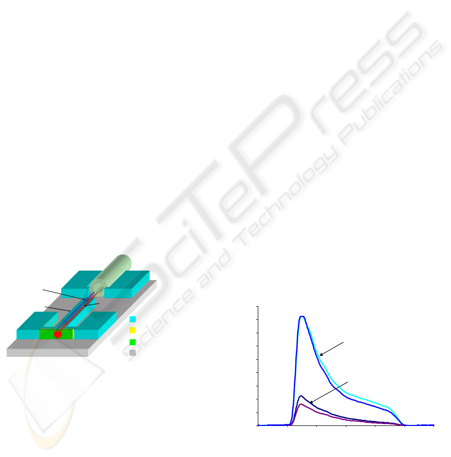
Fig. 3 shows the dynamic response. Both responses
demonstrate that biological recognition occurred and
was transduced to a mechanical signal.
4 OPTICAL BIOSENSOR
4.1 Design
Our design for the biophotonics platform is shown in
Fig. 4 (Powers et al., 2005). A thick photosensitive
polymer, SU-8, is used to define both the fluidic
channel and the optical waveguide on a pyrex
substrate. SU-8 is ideal for this application due to its
chemical inertness, ability to be spun very thick, and
high optical transmission for visible wavelengths.
Pyrex is chosen due to its smaller index of refraction
compared to the SU-8 (1.47 to 1.59). As shown in
the schematic, excitation light is applied through the
same optical fiber which collects the fluorescence
emission through the use of an off-chip bi-
directional coupler. In order to maximize the
collection efficiency at the waveguide facet, the
chitosan is deposited onto the sidewall of the SU-8
channel. A film of indium tin oxide (ITO) is chosen
to facilitate this deposition. Indium tin oxide is
conductive and mostly transparent to visible
wavelengths. The height of the SU-8 is chosen to be
110 μm in order to adequately couple the emitted
fluorescence into a multimode fiber with a core
diameter of 62.5 μm.
Optical
Path
Electrode (ITO)
Chitosan
Pyrex
Emission
Fluid Channel
Optical Fiber
Fiber Holder
Polymer (SU-8)
Waveguide
Excitation
Waveguide
Figure 4: Schematic of the optical biosensor.
4.2 Fabrication
Gold electrodes are initially patterned on a 4 inch
pyrex wafer using standard lithography techniques.
Prior to the addition of the SU-8, an adhesion
promoter AP300 (Silicon Resources, USA) is spun
on the wafer and baked on a hotplate in order to
improve the adhesion between the SU-8 and the
pyrex. SU-8 is spun to a thickness of 110 μm and
patterned to create the waveguides and fluidic
channel. Indium tin oxide is deposited using
magnetron RF sputtering to achieve a final thickness
of 200 nm. The sidewall of ITO is created by
patterning AZ9245 photoresist over the features on
the wafer and etching away the exposed ITO in a 1:1
HCl:DI water solution. In order to functionalize the
ITO surface, the wafer is submerged in a chitosan
solution at a pH of 5.07 (Sigma-Aldrich, USA)
while a voltage bias of 2 VDC is applied to the
electrodes. After 15 minutes, a film of chitosan on
the order of a few microns thick is deposited onto
the ITO electrode. The wafer is rinsed with DI water
to remove any excess residues. An optical fiber is
aligned to the output waveguide by a patterned fiber
clamp structure and is glued in place using UV-
curable epoxy. The index-matching epoxy fills the
gap between the fiber and the waveguide to
eliminate losses due to reflections.
4.3 Testing and Results
The optical biosensor was tested in response to
attachment of probe DNA and to hybridization with
target DNA (Badilita et al., 2007). Amine labeled
fluorescent probe DNA is attached to the chitosan by
glutaraldehyde crosslinking. The optical output was
measured by using an optical spectrum analyzer.
Fig. 5 shows the spectrum of the output signal
collected through the waveguide from probe DNA
labeled with Alexa Fluor 633. The emission signal is
filtered by a band pass filter with cutoff at 660nm.
The signal was measured before and after DNA
attachment. There is a clear increase in the measured
intensity due to the fluorescence signal from the
attached probe DNA.
Spectral Response to DNA Functionalization
0
500
1000
1500
2000
2500
3000
3500
4000
4500
640 660 680 700 720 740 760
Wavelength (nm)
Intensity (A. U.)
1) DNA Signals
2) Background Signals
Figure 5: Spectra of optical emission signals received both
1) after introduction of fluorescent DNA and 2) when no
fluorophores are present.
CHITOSAN FOR MEMS - Demonstration of Micromechanical and Optical Biosensors
111
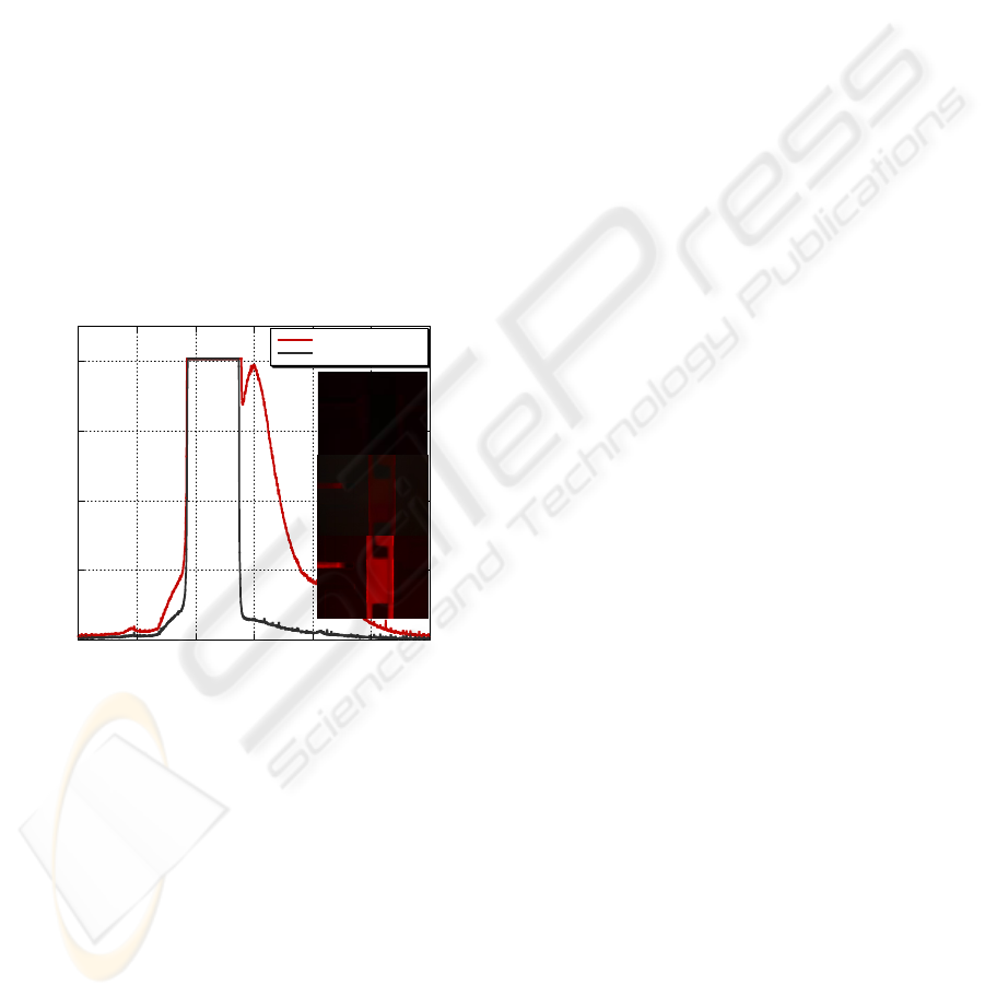
For the DNA hybridization experiments, the
chitosan surface functionalized with probe DNA was
exposed to matching or mismatching DNA solutions
for 30 min at room temperature. In order to
emphasize the selectivity, the mismatching DNA
was twice as concentrated (8 μM) as the matching
DNA (4 μM). Both DNA sequences were labeled at
the 5’ end with AlexaFluor 633 fluorophore. The
response was analyzed with a fluorescence
microscope and a spectrum analyzer.
Fig. 6 displays the intensity response to both
matching and mismatching DNA sequences. A
strong emission signal with a peak at about 650 nm
is demonstrated only for the matching DNA
sequence. The images on the right of the figure
display the fluorescence microscope images of the
sensor area after subjection to both the matching and
mismatching DNA. These results were also
demonstrated to be repeatable using the same device
by washing away the target DNA with a 4 M urea
solution at 95
o
C for 30 min and reintroducing the
DNA samples.
0
1000
2000
3000
4000
500 550 600 650 700 750 800
1-Matching DNA
1-Mis-Matching DNA
INTENSITY [a.u.]
WAVELENGTH [nm]
(a)
(b)
(c)
Figure 6: Collected output spectra demonstrating
successful DNA hybridization. Inset: fluorescence
microscope images of device: (a) after probe DNA
attachment (b) after mismatching target DNA (c) after
exposure to matching target DNA.
5 CONCLUSIONS
Chitosan enables a wide range of applications due to
its unique structure and relative abundance in nature.
We have reported the successful design, fabrication
and testing of two distinct MEMS biosensors which
utilize chitosan as a functionalization layer. Our
microcantilever has a deposited film of chitosan on
its surface to facilitate attachment of probe DNA. Its
structure allows for highly sensitive detection due to
mass loading. Our biophotonics sensor utilizes a
novel sidewall pattern of chitosan to improve
fluorescence emission capture into a planar
waveguide. DNA hybridization experiments have
been successfully performed with both devices. By
bridging the world of MEMS with the world of
biology through mechanical or optical detection,
chitosan forms the missing link allowing for more
robust and selective biological sensors.
ACKNOWLEDGEMENTS
This work was funded by the Laboratory for
Physical Sciences, the National Science Foundation,
and the R. W. Deutsch Foundation.
REFERENCES
Badilita, V., Shamim, I., Yi, H., Koev, S. T.,
Gerasopoulos, K. & Ghodssi, R. (2007) Chitosan-
Mediated Biomems Platform For Optical Sensing. The
14th International Conference On Solid-State Sensors,
Actuators, And Microsystems (Transducers '07). Lyon,
France.
Geng, R., Zhao, G., Liu, M. & Li, M. (2008) A Sandwich
Structured Sio2/Cytochrome C/Sio2 On A Boron-
Doped Diamond Film Electrode As An
Electrochemical Nitrite Biosensor. Biomaterials, 29,
2794.
Koev, S. T., Powers, M. A., Yi, H., Wu, L.-Q., Bentley,
W. E., Rubloff, G. W., Payne, G. F. & Ghodssi, R.
(2007) Mechano-Transduction Of Dna Hybridization
And Dopamine Oxidation Through Electrodeposited
Chitosan Network. Lab On A Chip, 7, 103-111.
Mizutani, F. (2007) Biosensors Utilizing Monolayers On
Electrode Surfaces. Sensors And Actuators B, 130, 14-
20.
Powers, M. A., Koev, S. T., Schleunitz, A., Yi, H.,
Hodzic, V., Bentley, W. E., Payne, G. F., Rubloff, G.
W. & Ghodssi, R. (2005) A Fabrication Platform For
Electrically Mediated Optically Active
Biofunctionalized Sites In Biomems. Lab On A Chip,
5, 583-586.
Yi, H., Wu, L.-Q., Bentley, W. E., Ghodssi, R., Rubloff,
G. W., Culver, J. N. & Payne, G. F. (2005)
Biofabrication With Chitosan. Biomacromolecules, 6,
2881-2894.
BIODEVICES 2009 - International Conference on Biomedical Electronics and Devices
112
