
DESIGN OF ANALOG SIGNAL PROCESSING INTEGRATED
CIRCUIT FOR MULTI-CHANNEL BIOMEDICAL STRAIN
MEASUREMENT INSTRUMENT
Wenchao Qu, Syed K. Islam
Department of Electrical Engineering, The University of Tennessee, 1508 Middle Dr., Knoxville, TN 37996, USA
Gary To, Mohamed R. Mahfouz
Center for Musculoskeletal Research,The University of Tennessee, 1414 Circle Dr., Knoxville, TN 37996, USA
Keywords: Analog digital conversion, SAR ADC, instrumentation amplifier, strain measurement, biomedical
instrumentation.
Abstract: An analog signal processing integrated circuit for micro-cantilever array is designed for strain measurement
in biomedical applications. The chip includes an analog multiplexer, an instrumentation amplifier, a sample
and hold circuit, an on-chip voltage and current reference, a successive approximation register analog-to-
digital converter and a digital control unit. The 8-bit ADC attains 45.4 dB signal-to-noise-and-distortion
ratio and 56.4 dB spurious-free-dynamic-range while operating at 772 KHz. The chip occupies an area of
1.54 mm
2
and consumes 17.8 mW power with a single 3.3 V supply. The chip has been fabricated in a
0.35μm 2-poly 4-metal CMOS process technology.
1 INTRODUCTION
The use of prosthetic joint implants to treat patients
with severe osteoarthritis and other joint
degenerative diseases began in the early 70s. During
the knee joint implant surgery, surgeons need to
perform accurate resections depending on various
instruments such as spacer block, tensioner and tram
adapter. These instruments provide valuable
information about the gap shape and size during the
bone resection process. However, the feedback of
instrument such as the spacer block is qualitative
and the degree of tightness of the ligaments is
inaccessible.
A new space blocker, shown in figure 1, is
designed by fully taking advantage of the sensors,
the ASIC and the telemetry technology. The sensors
and chips are on the surface with a battery inside the
spacer block, and the antenna is also designed to fit
in the handle. The surface of the instrument was
encapsulated by epoxy with fully FDA compliance.
In this paper, we mainly present the design of an
analog signal processing IC for biomedical strain
measurement system. In Section 2, we briefly
introduce the system design and then present the
circuit design in detail in Section 3. The
measurement results are given in Section 4, followed
by a summary in Section 5.
Figure 1: 3-D model of spacer block with embedded chip
and sensor array.
2 SYSTEM OVERVIEW
The system block diagram is shown in figure 2. The
system can be partitioned into three parts based on
256
Qu W., K. Islam S., To G. and R. Mahfouz M. (2008).
DESIGN OF ANALOG SIGNAL PROCESSING INTEGRATED CIRCUIT FOR MULTI-CHANNEL BIOMEDICAL STRAIN MEASUREMENT INSTRU-
MENT.
In Proceedings of the First International Conference on Biomedical Electronics and Devices, pages 256-259
DOI: 10.5220/0001049202560259
Copyright
c
SciTePress
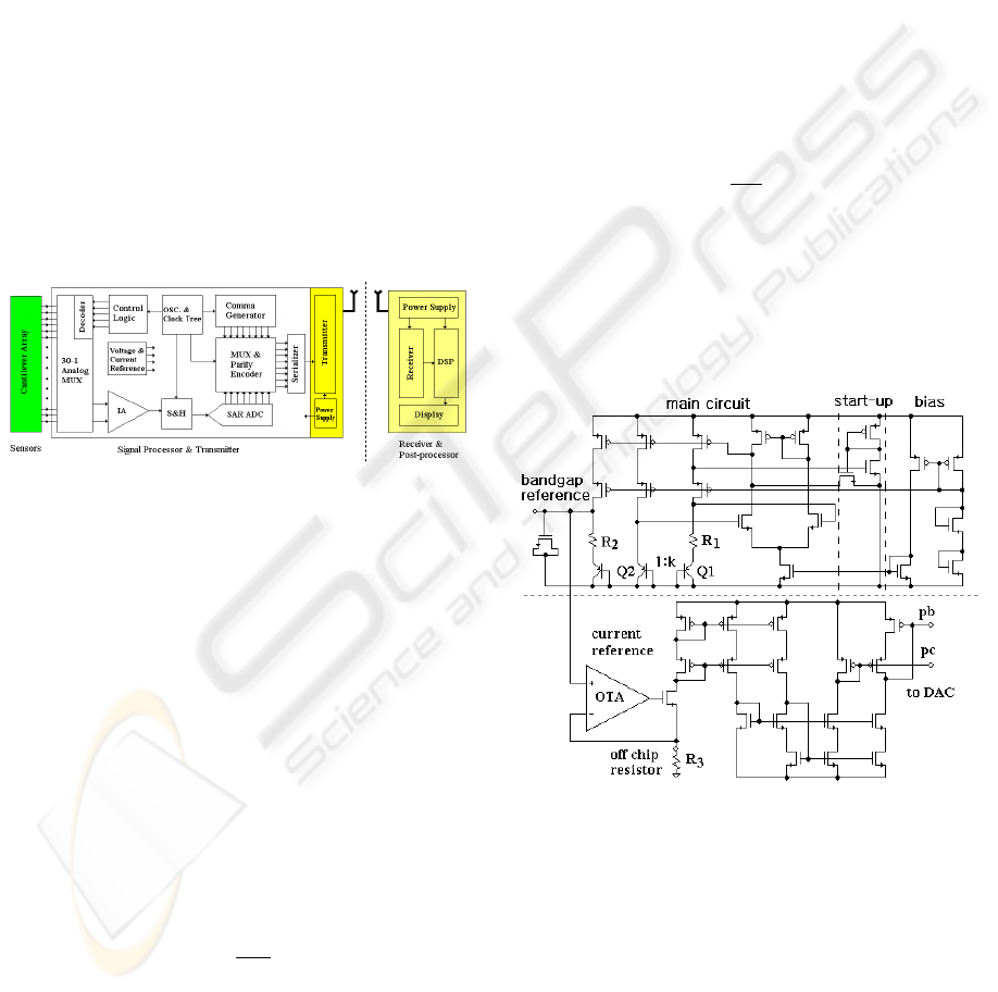
their functions. The first part is the sensor array.
There are 30 strain-sensing micro-cantilevers
distributed evenly on the two sides of the biomedical
instrument top plate. The Wheatstone bridge
configured sensors convert the physical strain to a
resistance change and then to voltage signal under
DC excitation. The middle part shown in figure 2
includes two chips, one chip for signal processing
and another one for signal transmitting. The signal-
processing chip amplifies the signal coming from the
sensors and digitizes the analog signal to digital
domain. The transmitter chip sends out the signal
using ASK modulation with 335MHz carrier
frequency. The receiver part receives and recovers
the data remotely. Furthermore, the data will be
post-processed by software and shown graphically
on the display.
In this paper, the scope mainly focuses on the
design and implementation of the signal processing
integrated circuit.
Figure 2: Sensor array signal processing system block
diagram.
3 CIRCUIT IMPLEMENTATION
Instrumentation Amplifier. The Instrumentation
Amplifier (IA) amplifies the difference signal
between the two input terminals and rejects the
common mode signals on both inputs (Kitchin and
Counts, 2000). Unlike normal opamp, the feedback
of IA uses an internal resistance network but the
gain is set by an external resistor.
The external gain setting resistor provides
maximum design flexibility for the system designer
to accommodate the input signal level. The gain can
be set using the following equation
g
V
R
R
A
2
1+=
(1)
where, R is internal resistor and R
g
is off chip gain
setting resistor.
A classical 3 opamps configuration is chosen and
an additional opamp provides variable output DC
level to accommodate the following stage circuit.
Voltage and Current Reference. Both the ADC
and the DAC in the system need either the voltage or
the current reference. Bandgap voltage reference is
selected for its extraordinary performance of
process, power supply and temperature variation
independence (Meyer and Gray, 1993, Brokaw,
1974). The reference is generated by adding a
negative temperature coefficient (TC) voltage and a
weighted positive TC voltage. Hence, a zero TC can
be achieved by adjusting the value of R2 and R1
based on the following equation
kV
R
R
VV
TbeBG
ln
1
2
+=
(2)
where, V
be
is the base-emitter junction voltage, V
T
is
thermal voltage and k is the geometry ratio of Q1
and Q2. The bandgap reference circuit shown in
figure 3 has two operation points. To guarantee the
circuit always works at the right point, a startup
circuit is also included.
Figure 3: Voltage and Current Reference Schematic.
The current reference for the current-steering
DAC cannot be fully generated on-chip due to the
lack of a high precision absolute value resistor. With
the aid of a low TC and high precision external
resistor, and the bandgap voltage reference, an
accurate current reference can be obtained. The
current reference circuit is shown in the lower part
of figure 3.
DESIGN OF ANALOG SIGNAL PROCESSING INTEGRATED CIRCUIT FOR MULTI-CHANNEL BIOMEDICAL
STRAIN MEASUREMENT INSTRUMENT
257
Sample and Hold. In order to relax the dynamic
requirements for the ADC, a sample and hold circuit
is inserted between the amplifier and the ADC
(Waltari and Halonen, 2002). The sample and hold
grabs the fast changing signal and stores it in the
sampling capacitor Cs. In the meantime, the thermal
noise is also trapped into the capacitor during the
turning off of the switch. For an 8-bit ADC, the
minimum required sampling capacitor Cs can be
calculated by the following equation
2
n
B
fS
V
Tk
nC =
(3)
where, k
B
is Boltzmann constant, T is absolute
temperature, V
n
2
is quantization noise power, and the
coefficient n
f
models the noise from the amplifier
and has a value between 0~1. In (3), we assume that
the quantization noise power is equal to the thermal
noise power.
The settling error for linear one pole settling is
expressed as
SSSS
dB
CRff
r
ee
2
1
2
3
−
−
==
−
ω
ε
(4)
where, f
S
is sampling frequency and R
S
is the
equivalent on-resistance of sampling switch. The
maximum allowed settling error for 8-bit ADC is
0.39%. Then the equivalent resistance for the switch
can be calculated by
r
SS
S
Cf
R
ε
1
ln
1
2
1
=
(5)
where, ε
r
is settling error. Once we know the
minimum equivalent on-resistance of the switch, the
switch size can be determined by the transistor
parameters.
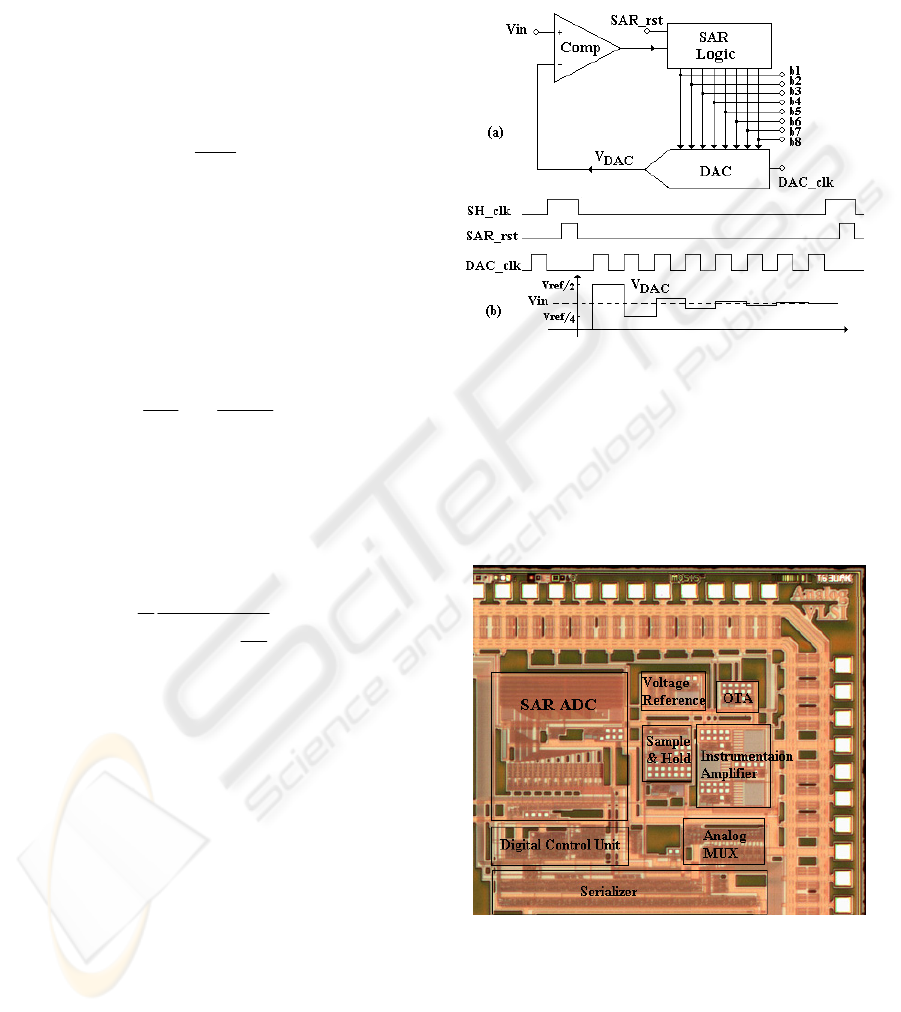
SAR ADC. The Successive Approximation
Register (SAR) ADC (Scott et al., 2003) is selected
as the data conversion unit for several reasons. First,
the SAR ADC is suitable for moderate speed and
moderate resolution data conversion. Also, the SAR
ADC is extremely power and area efficient. The
SAR ADC shown in figure 4 has three parts:
comparator, SAR logic (Anderson, 1972) and DAC.
The conversion mechanism behind the SAR ADC is
similar to binary search algorithm. First, the DAC
MSB is set to 1 while all other bits are set to 0, then
converted to analog domain and compared with the
stored input signal. Then the SAR logic will keep or
reset the MSB signal based the comparison result.
The procedure is iterated until the LSB is resolved.
Apparently, the conversion time is 8 periods for an
8-bit ADC plus 1 period for sampling. The timing
and conversion procedure is shown in figure 4b.
Figure 4: SAR ADC block and timing diagram.
4 EXPERIMENTAL RESULTS
Figure 5 shows the signal process chip micrograph.
The core die area (excluding the pad and ESD
circuit) is about 1.54 mm
2
.
Figure 5: Chip prototype micrograph.
The voltage gain frequency response of the IA is
shown in figure 6 for three different external gain
setting resistors. The unity gain bandwidth for
different voltage gain is almost fixed and has a value
about 2.5 MHz.
BIODEVICES 2008 - International Conference on Biomedical Electronics and Devices
258
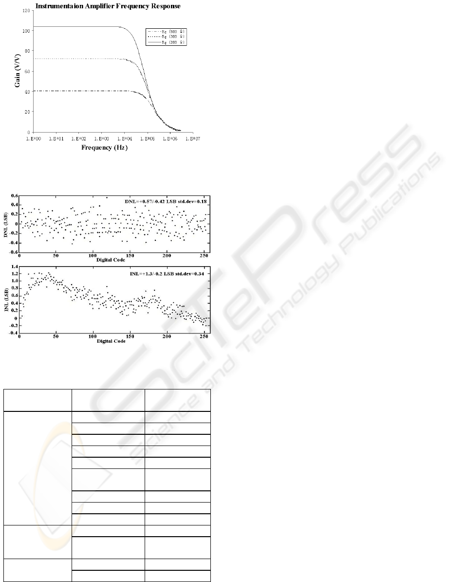
Figure 6: Voltage gain frequency response of
instrumentation amplifier.
Figure 7: Integral and differential nonlinearity of ADC.
Table 1: Prototype chip performance summary.
Parameter Value
ADC
Resolution 8 bit
ENOB 7.24 bit
SNDR 45.4 dB
SFDR 56.4 dB
Conversion Rate 772 KHz
DNL +0.57/-0.42
LSB
INL +1.3/-0.2 LSB
Area 0.43 mm
2
Power 17.8 mW
Instrumentation
Amplifier
Voltage Gain 20~200 V/V
Unity Gain
Bandwidth
2.5 MHz
Total Area 1.54 mm2
Power 17.8 mW
The DNL and INL of the SAR ADC are obtained
by histogram testing (Plassche, 2003) and are shown
in figure 7. The DNL is 0.57/-0.42 LSB and INL is
1.3/-0.2 LSB with zero missing code. Parts of the
test results are summarized in table 1.
5 CONCLUSIONS
The prototype chip presented here was fabricated in
a 0.35 μm 2-poly 4-metal CMOS process. The
operating voltage is 3.3 V and the chip can also
work for the voltage range of 2.6 V ~ 4 V. The area
of the chip (core area) is 1.54 mm2, and consumes
5.4 mA current. The measurement results of the
signal processing chip verify the design concept and
meet the specifications for the biomedical
instrument system. A wireless strain measurement
instrument is being developed based on this chip
design.
REFERENCES
Anderson, T. O. (1972) Optimum Control Logic for
Successive Approximation AD Converters. Computer
Design, 11, 81-86.
Bienstman, L. A. & De Man, H. J. (1980) An eight-
channel 8 bit microprocessor compatible NMOS D/A
converter with programmable scaling. Solid-State
Circuits, IEEE Journal of, 15, 1051-1059.
Brokaw, A. P. (1974) A simple three-terminal IC bandgap
reference. Solid-State Circuits, IEEE Journal of, 9,
388-393.
Kitchin, C. & Counts, L. (2000) A Designer's Guide to
Instrumentation Amplifiers. Analog Devices.
Meyer, R. G. & Gray, P. (1993) Analysis and design of
analog integrated circuits, Wiley.
Plassche, R. J. V. D. (2003) CMOS integrated analog-to-
digital and digital-to-analog converters, Boston,
Kluwer Academic Publishers.
Scott, M. D., Boser, B. E. & Pister, K. S. J. (2003) An
ultralow-energy ADC for Smart Dust. Solid-State
Circuits, IEEE Journal of, 38, 1123-1129.
Waltari, M. E. & Halonen, K. A. I. (2002) Circuit
techniques for low-voltage and high-speed A/D
converters, Boston, Kluwer Academic Publishers.
DESIGN OF ANALOG SIGNAL PROCESSING INTEGRATED CIRCUIT FOR MULTI-CHANNEL BIOMEDICAL
STRAIN MEASUREMENT INSTRUMENT
259
