
DESIGN AND IMPLEMENTATION OF AN FPGA-BASED
SVPWM IC FOR PWM INVERTERS
Cheng-Hung Tsai
Department of Electrical Engineering, China Institute of Technology
245 Yen-Chiu Yuan Road, 3rd Sec., Taipei, 11581, Taiwan
Hung-Ching Lu
Department of Electrical Engineering, Tatung University
40 Chungshan North Road, 3rd Sec., Taipei, 10451, Taiwan
Keywords: FPGA, SVPWM IC, High-performance.
Abstract: This paper presents a new circuit design scheme of the space-vector pulse-width modulation (SVPWM)
strategy, including linear and overmodulation ranges. The proposed scheme has been developed using the
state-of-the-art field-programmable gate array (FPGA) technology. The SVPWM control integrated circuit
(IC) can be realized by using only a single FPGA (Cyclone) from Altera, Inc. Experimental results show
that this controller can present an excellent drive performance and its switching frequency, which can be set
to over 100kHz, is adjustable as well as its deadtime. The output fundamental frequency can be adjusted
over 2000Hz. This SVPWM IC can be included in the digital current control loop for stator current
regulation. The IC also provide a simple hardware and low cost for high-performance ac drives.
1 INTRODUCTION
In engineering practice, because of the complexity
of servo control algorithm, it is usually implemented
with software based on DSP (Lai and Chang, 1999)
(Marwali et al., 1999) (Ma et al., 2001) (Zadeh,
2001). This approach can provide a flexible control
scheme, but suffers from a long period of
development and exhausts many resources of the
CPU. In some cases, dual DSPs have to be adopted
to achieve superior performances (Tzou et al., 1996)
(Tzou et al., 1996b) (Tzou et al., 1996c). Such
additional hardware and software design for such a
dual-DSP controller will complicate the design
process enormously.
In recent years, a novel design methodology
has arisen, that is FPGA-based hardware
implementation technology (Carrica et al., 2003)
(Man et al., 1995) (Lin et al., 2005) (Zeidman et al.,
2002) (Tonelli et al., 2001). Because of the
programmable characteristics of FPGA and IP cores,
users can design their application-specific integrated
circuit (ASIC) in lab according to their schemes,
instead of participation of the semiconductor
manufacturer. In addition, since FPGA can carry out
parallel processing by means of hardware mode,
which occupies nothing of the CPU, a very high
speed level of the system can be obtained as well as
an exciting precision. This novel design
methodology has now been used in high
performance motion control field, such as (Tonelli et
al., 2001) (Tzou and Hsu, 1997) (Zhou et al., 2004).
Literature (Tonelli et al., 2001) proposed a universal
SVPWM controller with overmodulation and
deadtime compensation, but it is not a flexible
design and its switching frequency can not be set
arbitrarily; besides it also needs an extra EPROM for
sin and cosine values as a lookup table. In (Tzou and
Hsu, 1997), the constructed IC has a strong function
but it does not include overmodulation range and
also needs additional EPROM. In (Zhou et al.,
2004), the switching frequency can only be set to 40
kHz maximum.
Employing FPGA to realize PWM strategies
provides advantages such as rapid prototyping,
simple hardware, software design and very high
switching frequency. Thus, the realization of the
347
Tsai C. and Lu H. (2007).
DESIGN AND IMPLEMENTATION OF AN FPGA-BASED SVPWM IC FOR PWM INVERTERS.
In Proceedings of the Fourth International Conference on Informatics in Control, Automation and Robotics, pages 347-353
DOI: 10.5220/0001620203470353
Copyright
c
SciTePress
SVPWM schemes by state-of-the-art FPGA
technology is the best way to improve the bandwidth
of the current or speed controller. This paper
proposed a simple hardware FPGA-based control
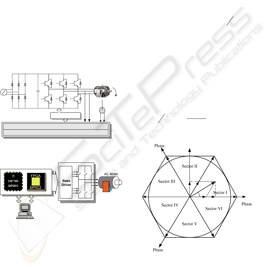
structure for ac drives depicted in Fig. 1 and
develops a high performance realization scheme for
the SVPWM control IC employing a single FPGA
(Cyclone) from Altera, Inc.
The designed IC can serve either for ac motor
drives or three-phase ac-voltage regulation systems.
It can also be incorporated as part of the digital
current loop for ac drives. Fig. 2 shows the circuit
configuration of a DSP-controlled ac drive using the
SVPWM control IC. The rest of this paper is
organized as follows. Section II briefly introduces
the principle of the space-vector PWM method.
Section III discusses developing a strategy for the
hardware design scheme. Section IV implements the
circuits on a low cost FPGA and shows the
experimental results. In section V some conclusions
are drawn.
FPGA
A/D Converter
Vdc
Gate Drive
encoder
b
i
a
i
1
S
6
S
5
S
3
S
4
S
2
S
Figure 1: Circuit schematics of a voltage-source full
bridge three-phase PWM inverter.
Figure 2: Circuit configuration of the DSP-controlled
FPGA-based PWM current controller for the ac drive.
2 PRINCIPLE OF SVPWM
The main purpose of the PWM inverter is to
generate a variable-voltage variable-frequency
(VVVF) three-phase voltage to the ac motor.
Conventional sinusoidal PWM employs several
kinds of sampling methods with sinusoidal signals
according to a carrier signal, e.g., natural sampling
(Schonung and Stemmler, 1964) (Pollack, 1972), or
symmetric or asymmetric regular sampling (Bowers,
1975).
The principle of the SVPWM is more clearly
explained by representing a space vector (Park,
1929). The motor stator voltage vector can be
expressed as a combination of the inverter output-
phase voltage
a
V
,
b
V
,
c
V
which can be described in
vector form as:
cbas
VVVV
αα
++=
2
K
,
)
3
2
exp(
π
α
j=
(1)
where
)120sin(
)120sin(
sin
D
D
+=
−=
=
wtVV
wtVV
wtVV
dc
db
da
and
d
V
is the amplitude of the fundamental
component. As shown in Fig. 3, there are eight
voltage vector configurations of the three-phase
PWM inverter. Their corresponding voltage vectors
are expressed as:
6,...,2,1,
3
)1(
exp
3
2
=
⎥
⎦
⎤
⎢
⎣
⎡
−
= n
n
jVV
dn
π
K
(2)
0
07
=
=
VV
(3)
α
β
1
V
K
6
V
K
5
V
K
4
V
K
3
V
K
2
V
K
7
V
K
0
V
K
ref
V
K
1
V
′
K
2
V
′
K
a
b
c
θ
α
U
β
U
Figure 3: Voltage space vector diagram.
The stator voltage vector can be decomposed of a
combination of two basic vectors, as Fig. 3 indicates.
The advantage of the SVPWM strategy is the
minimization of harmonic distortion in the current
ICINCO 2007 - International Conference on Informatics in Control, Automation and Robotics
348
by selecting the appropriate switching vectors and
determination of the corresponding dwelling widths.
If the reference vector
ref
V
K
is located in sector I,
then it is composed of voltage vector
1
V
,
2
V
, and
zero voltage vectors
7
V
and
0
V
as illustrated in Fig.
3. The flux produced by the reference voltage vector
in a PWM switching period is a combination of each
individual flux produced by its corresponding
voltage vector. The relationships of the voltage
vector can be expressed as:
∫∫∫∫∫
+++=
7210
0
7
0
2
0
1
0
0
0
.
TTTTT
ref
dtVdtVdtVdtVdtV
s
(4)
Because the voltage vectors
1
V
and
2
V
are basic
vectors and
0
V
and
7
V
are zero vectors, that gives
ss
ref
T
T
V
T
T
VV
2
2
1
1
+=
(5)
Where
s
T
is the switching period and
1
T
,
2
T
are the dwelling time of
1
V
and
2
V
,
respectively. This voltage space vector can
be expressed in rectangular coordinates as
follows:
⎥
⎦
⎤
⎢
⎣
⎡
⋅⋅=
⎥
⎥
⎦
⎤
⎢
⎢
⎣
⎡
⋅⋅⋅+
⎥
⎦
⎤
⎢
⎣
⎡
⋅⋅⋅
θ
θ
sin
cos
3
2
2
60sin
60cos
3
2
0
1
3
2
21
MV
T
VTVT
d
s
dd
D
D
(6)
Where
d
ref
V
V
M
3
2
=
,
D
600 ≤≤
θ
, and the
dwelling time of each vector can be got.
D
D
60sin
)60sin(
2
1
θ
−
⋅⋅= M
T
T
s
(7)
D
60sin
)sin(
2
2
θ
⋅⋅= M
T
T
s
(8)
2170
2
TT
T
TT
s
a
−−==
. (9)
If the calculated value
s
TTT >+
21
, i.e., the zero
vector time is minus, overmodulation occurs and the
duration time should be processed again. To
improve the resolution of the binary divider, the new
time can be reconsidered as follows:
If
21
TT >
, then
′
−=
′
+
=
′
12
21
1
1
2
,
2
T
T
T
T
TT
T
T
ss
(10)
otherwise
′
−=
′
+
=
′
21
21
2
2
2
,
2
T
T
T
T
TT
T
T
ss
(11)
3 DESIGN OF THE FPGA-BASED
SVPWM IC
Many factors need to be considered in designing the
PWM control IC, such as simplicity, flexibility, and
complexity of the circuit design. In practical
applications, the PWM IC is not possible to
corporate with a conventional microprocessor,
therefore, the control IC is stand alone. The major
design goal is to relieve the microprocessor from
time-consuming computational tasks such as PWM
signal generating, deadtime compensation , and
current control.
Figure 4: Functional block diagram of the programmable
FPGA-based SVPWM IC.
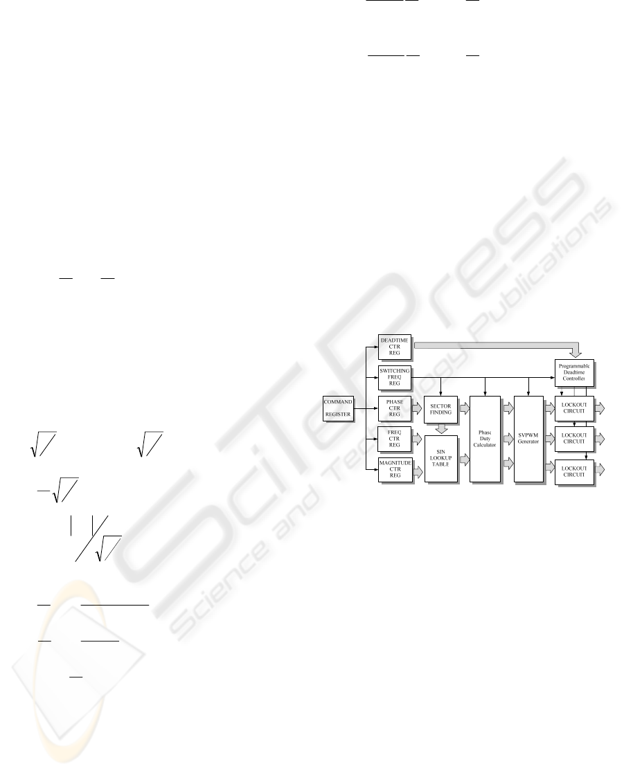
Fig. 4 depicts the block diagram of a proposed
programmable FPGA-based SVPWM control IC.
This design consists of five registers for the
command frequency, modulation factor, phase of the
stator voltage vector, the switching frequency of the
PWM and the deadtime for the power module.
To simplify the interface circuit, the commands of
these five registers are downloaded from the
computer directly. The control parameters can be set
in the original project file. The internals of the
designed IC consist of a sin-table address decoder, a
duty-ratio calculator, a PWM waveform generator
and a programmable deadtime register. The firing
time width of an SVPWM waveform involves
computing of sin function. Therefore, arithmetic
computational methods and the bit length for
manipulating data are important factors in designing
the digital hardware for the SVPWM. Floating-point
arithmetic complicates the approach to hardware
DESIGN AND IMPLEMENTATION OF AN FPGA-BASED SVPWM IC FOR PWM INVERTERS
349
design greatly; only positive integer arithmetic can
provide a feasible solution. In this paper, all positive
integer arithmetic without external EPROM sin-table
reference has been adopted for the digital realization
of the SVPWM IC.
The simple requirements for realizing the SVPWM
scheme is to first compute the time width of each
voltage vector. Second, these three-phase PWM
waveforms are converted to centralized PWM
waveforms. Finally, the PWM gating signals are
inserted with adjustable time delay to protect the
power module from short circuit.
The specified voltage amplitude, frequency,
switching frequency, initial phase and deadtime are
set in the VHDL file or received from DSP to
produce the three-phase PWM gating signals. The
sin reference is recorded in the built in memory of
the FPGA for the PWM duty-ratio generator.
In ideal conditions, the gating signals to the power
switches of same phase leg of the PWM inverter
should be complementary. However, in order to
avoid short circuit in the power semiconductors, an
appropriate delay time must be inserted between
these two gating signals. The length of this deadtime
is depending on the characteristic of adopted IGBT
module. Typically the deadtime is set to 2~4
us
. A
programmable deadtime controller is included in the
designed SVPWM IC, which greatly facilitates its
practical applications.
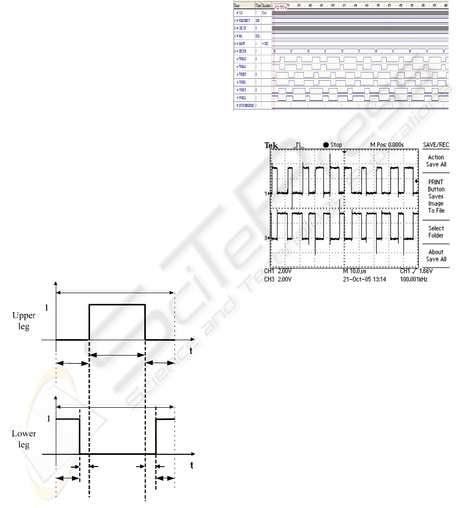
ON
T
OFF
T
s
T
s
T
OFF
T
ON
T
ON
T
tΔ tΔ
Figure 5: Timing diagram of the PWM signal with
deadtime.
The PWM signal waveforms and their
corresponding delay signals are described in Fig. 5.
The
t
Δ
is the specified deadtime. The deadtime
controller generates the gating signals to the
registers, which includes a digital comparator and
results in PWM signals with a specified time delay.
Fig. 6 shows simulation results of the programmable
FPGA design for the PWM waveform.
(a)
PWMAU
PWMAL
(b)
Figure 6: Simulation and experimental results of the
voltage vector to three-phase PWM duty ration converter
at switching frequency is 100kHz and the output
frequency is 1800Hz.
4 HARDWARE
IMPLEMENTATIOAND
EXPERIMENTAL RESULTS
For the realization of the proposed SVPWM scheme,
cost and speed considerations led to selecting an
SRAM-based FPGA Cyclone EP1C3 from Altera,
Inc. for realizing of the SVPWM IC. The EP1C3 has
around 2910 logic gates, 60k RAM bits, and 1
phase-locked loop (PLL). The internal clock can
operate at 200 MHz. Some important specifications
of the EP1C3 are listed in Table I. Altera also
provides EDA tools (Quartus II) for the development
of ASIC’s employing FPGA’s. The Quartus II
consists of a schematic entry editor, an interface
with the schematic entry editor, logic and timing
ICINCO 2007 - International Conference on Informatics in Control, Automation and Robotics
350

simulation software, and design implementation
software. The logic and timing simulation software
is especially relevant to the design of complicated
digital circuits because it is best suited to resolve
circuit problems during the early design stage.
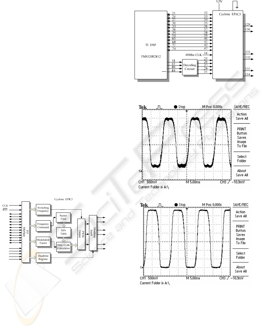
Fig. 7 illustrates the pin assignment of the
designed SVPWM IC. The SVPWM modules are all
described with VHDL and synthesized with Synplify
software. The designed IC can operate at 200Mhz
system clock by using the internal PLL, and the
switching frequency as well as deadtime is
adjustable. Fig. 8 is the circuit configuration of the
SVPWM IC employing a single-chip DSP
(TMS320F2812) from Texas Instruments. The
simplicity in the interface circuit design illustrates its
feasibility for practical applications. The IC can
construct a current loop, and it can also be
considered as an IP core which can be integrated
into a system on one chip (SOC) with other IP cores.
Fig. 9 illustrates the experimental results of the
phase voltage of the SVPWM gating signals from
linear to overmodulation region. The output
fundamental frequency can be adjusted for over
2000Hz. Such a wide frequency control range, with
high-frequency switching, is only feasible by
utilizing the state-of-the-art VLSI digital circuit
design technique. In this designed IC, the SVPWM
scheme is finished in 70 clocks. It means the whole
software takes only 350
ns
. Therefore, the PWM
switching frequency can be set for over 100kHz. The
deadtime for the PWM gating signals is also
adjustable. The PWM waveforms with deadtime are
shown in Fig. 10 by using Tektronix oscilloscope.
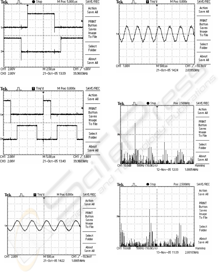
Fig. 11 shows the experimental results of the
designed SVPWM IC used in a PWM inverter ac
motor drive with 1000 and 2000Hz output,
respectively. Experimental results show the
constructed SVPWM IC can generate a wide range
of output frequencies with controlled fundamental
voltage.
5 CONCLUSIONS
This paper presents the design and realization of a
programmable SVPWM control IC for high
performance ac servo drives. The SVPWM scheme
is implemented and tested by using an FPGA
technology. Simulation and experimental results are
provided to verify the implemented SVPMW control
IC. The designed IC is also easy to interface with
DSP or other IP cores to form a closed loop control
system. Besides, it doesn’t need external EPROM,
and the source codes can be easily replanted to
different FPGA’s without any changes. Given that an
economic manufacturing cost can be achieved, it is
believed that the PWM control IC’s will become the
important components in power converters and
motor drives of the future
.
ACKNOWLEDGEMENTS
This work was supported by the National Science
Council of the republic of China under the contract
of NSC 93-2213-E036-018.
REFERENCES
Y. S. Lai, and S. C. Chang, 1999, “DSP-based
implementation of new random switching technique of
inverter control for sensorless vector-controlled
induction motor drives,” IEE Proceedings- Electric
Power Applications, Vol. 146, No. 2, pp. 163-172.
M. N. Marwali, A. Keyhani, and W. Tjanaka, 1999,
“Implementation of indirect vector control on an
integrated digital signal processor-based system,”
IEEE Transactions on Energy Conversion, Vol. 14,
No. 2, pp. 139-146.
J. D. Ma, W. Bin, N. R. Zargari and S. C. Rizzo, 2001, “A
space vector modulated CSI-based AC drive for
multimotor applications,” IEEE Transactions on
Power Electronics, Vol. 16, No. 4, pp. 535-544.
S. V. Zadeh, 2001, “Variable flux control of permanent
magnet synchronous motor drives for constant torque
operation,” IEEE Transactions on Power Electronics,
Vol. 16, No. 4, pp.527-536.
Y. Y. Tzou, M. F. Tsai, Y. F. Lin and H. Wu, 1996, “Dual
DSP based fully digital control of an AC induction
motor,” Proceedings of the IEEE International
Symposium on Industrial Electronics, Vol. 2, pp. 673-
678.
Y. Y. Tzou, M. F. Tsai, Y. F. Lin and H. Wu, 1996, “Dual
DSP based fully digital control of an AC induction
motor,” Proceedings of the IEEE International
Symposium on Industrial Electronics, Vol. 2, pp. 673-
678.
Y. Y. Tzou, W. A. Lee and S. Y. Lin, 1996 , “Dual-DSP
sensorless speed control of an induction motor with
adaptive voltage compensation,” 27th Annual IEEE
Power Electronics Specialists Conference, Vol. 1, pp.
351-3.57.
D. Carrica, M. A. Funes and S. A. Gonzalez, 2003, “Novel
stepper motor controller based on FPGA hardware
implementation,” IEEE/ASME Transactions on
Mechatronics, Vol. 8, No. 1, pp. 120-124.
K. F. Man, Y. C. Ho, K. P. Cheuk and S. Kwong, 1995,
“Hardware implementation of variable pulse
frequency algorithm,” Electronics Letters, Vol. 31,
No. 10, pp. 839-840.
DESIGN AND IMPLEMENTATION OF AN FPGA-BASED SVPWM IC FOR PWM INVERTERS
351
F. J. Lin, D. H. Wang and P. K. Huang, 2005, “FPGA-
based fuzzy sliding-mode control for a linear induction
motor drive,” IEE Proceedings- Electric Power
Applications, Vol. 152, No. 5, pp. 1137-1148.
B. Zeidman and R. Zeidman, 2002, Designing with
FPGAs and CPLDs, Berkeley.
M. Tonelli, P. Battaiotto and M. I. Valla, 2001, “FPGA
implementation of an universal space vector
modulator,” The 27
th
Annual conference of the IEEE
Industrial Electronics Society, pp. 1172-1177.
Y. Y. Tzou and H. J. Hsu, 1997, “FPGA realization of
space-vector PWM control IC for three-phase PWM
inverters,” IEEE Trans. On Power Electronics, Vol.
12, No. 6, pp. 953-963.
Z. Zhou, T. Li, T. Takahashi and E. Ho, 2004, “Design of
a universal space vector PWM controller based on
FPGA,” IEEE Applied Power Electronics Conference
and Exposition, Vol. 3, pp. 1698-1702.
A. Schonung and H. Stemmler, 1964, “Static frequency
changers with subharmonic control in conjunction
with reversible variable speed ac drives,” Brown
Boveri Rev., Vol. 122, No. 5, pp. 555-577.
J. J. Pollack, 1972, “Advanced pulsewidth-modulated
inverter techniques,” IEEE Transaction on Industrial
Applications., Vol. IA-8, No. 2, pp. 145-154.
S. R. Bowers, 1975, “New sinusoidal pulse width
modulated inverter,” Proceedings of Industrial
Electrical Engineerings., Vol. 122, No. 5, pp. 514-
520.
R. M. Park, 1929, “Two-reaction theory of synchronous
machines part I: Generalized method of analysis,”
AIEE Trans., Vol. 48, pp. 716-730.
0
D
1
D
10
D
9
D
8
D
7
D
6
D
5
D
4
D
3
D
2
D
11
D
0
MS
1
MS
4
MS
2
MS
3
MS
PWMAU
PWMCL
PWMCU
PWMBL
PWMBU
PWMAL
Figure 7: Pin assignment of the FPGA-based SVPWM
control IC.
SVPWM
Control
IC
0
D
1
D
10
D
9
D
8
D
7
D
6
D
5
D
4
D
3
D
2
D
11
D
0
MS
1
MS
4
MS
2
MS
3
MS
PWMUH
PWMWL
PWMWH
PWMVL
PWMVH
PWMUL
WE
2
A
0
A
1
A
0
D
1
D
10
D
9
D
8
D
7
D
6
D
5
D
4
D
3
D
2
D
11
D
Figure 8: Circuit block diagram of the designedSVPWM
IC interface with a sing-chip DSP TMS320F2812.
(a)
(b)
Figure 9: Experimental phase voltage wave form in the (a)
linear region; (b) overmodulation region.
ICINCO 2007 - International Conference on Informatics in Control, Automation and Robotics
352
(a)
(b)
Figure 10: Experimental results of the programmable
delay time with (a) 2 and (b) 4 us, respectively.
(a)
(c)
Figure 11: Experimental results of the SVPWM IC used in
a PWM inverter drive with 1000- and 2000-Hz output: (a)
and (c) are the phase currents.
(b)
(d)
Figure 11: Experimental results of the SVPWM IC used in
a PWM inverter drive with 1000- and 2000-Hz output: (b)
and (d) are the corresponding frequency spectrum.
DESIGN AND IMPLEMENTATION OF AN FPGA-BASED SVPWM IC FOR PWM INVERTERS
353
