
The Visual Inspection of Solder Balls in Semiconductor Encapsulation
Conceic¸
˜
ao N. Silva
1
, Neandra P. Ferreira
2
, Sharlene S. Meireles
2
, Mario Otani
2
,
Vandermi J. da Silva
1
, Carlos A. O. de Freitas
1
and Felipe G. Oliveira
1
1
Institute of Exact Sciences and Technology (ICET), Federal University of Amazonas (UFAM),
Itacoatiara, Amazonas, Brazil
2
Cal-Comp, Institute of Research and Technological Innovation (ICCT), Manaus, Amazonas, Brazil
neandra pf@calcomp-icct.org.br, sharlene@calcomp-icct.org.br, mario otani@calcomp-icct.org.br
Keywords:
Ball Bond Inspection, Automatic Visual Inspection, Deep Learning.
Abstract:
The growing demand for increasing memory storage capacity has required a high density of integration within
the semiconductor encapsulation and, consequently, has made this process more complex and susceptible
to failures during the production stage. In the semiconductor encapsulation area, the costs of materials and
equipment are high and the profit margin is narrow, making it necessary to rigorously inspect the process steps
to keep the productive activity viable. This work addresses the problem of quality control in silicon wafers
soldering procedure, allowing error detection before the epoxy resin molding process, generating useful infor-
mation for correcting equipment configurations and predicting failures from the raw materials and inputs used
in the process. We propose an approach to classify solder balls, in the soldering process of silicon wafers on
Ball Grid Array (BGA), contained in the Printed Circuit Board (PCB) substrates. The proposed methodology
is composed of two main steps: i) Solder ball segmentation; and ii) Solder ball classification through deep
learning. The proposed predictive model learns the relation between visual features and the different soldering
conditions. Real and simulated experiments were carried out to validate the proposed approach. Results show
the obtained accuracy of 99.4%, using Convolutional Neural Network (CNN) classification model. Further-
more, the proposed approach presents high accuracy even regarding noisy images, resulting in accuracy of
92.8% and 75.7% for a Salt and Pepper and Gaussian noise, respectively, in the worst scenario. Experiments
demonstrate reliability and robustness, optimizing the manufacturing.
1 INTRODUCTION
Automated inspection of semiconductors has been the
focus of numerous research efforts in Microelectron-
ics and Industrial communities in the past few years
(Zhang et al., 2022). The semiconductors inspection
has the role of feeding back the methods with infor-
mation on specific errors, which can be correlated
with production problems. The semiconductors anal-
ysis includes the assessment on occurrence of failures
due to the materials involved in the process or inad-
equate definitions of the machine parameters (Zhang
et al., 2021).
In the semiconductors context, the production of
memory devices represents a great manufacturing
challenge, especially due to the small component’s di-
mensions and the required precision in its operation.
Additionally, the market demand for memory devices
has increased massively, requiring the expansion of
memory production volume, making the manual in-
spection process critical (Chang et al., 2018).
The use of the conventional visual inspection pro-
cess, regarding a trained human operator, presents ef-
fectiveness between 80% and 90% of cases. However,
after the first half working hour, the human operator
visual acuity decreases significantly, for the analysis
of a single type of defect [1]. In Figure 1, is pre-
sented an example of a human visual inspection of
silicon wafers, where the human operator should visu-
ally run through all the components on the PCB sub-
strate looking for different types of defects.
In this paper, we present an approach to clas-
sify solder balls, in the soldering process of a sili-
con wafer, called die, on BGAs, contained in the PCB
substrates. The solder ball is classified into three cat-
egories: i) correct; ii) absence; or iii) failure. We also
introduce a CNN architecture for supervised classifi-
cation of solder balls, which learns the main features
that represent all approached types of soldering condi-
tions. Experiments in real-world scenarios and simu-
750
Silva, C., Ferreira, N., Meireles, S., Otani, M., J. da Silva, V., O. de Freitas, C. and Oliveira, F.
The Visual Inspection of Solder Balls in Semiconductor Encapsulation.
DOI: 10.5220/0011357400003271
In Proceedings of the 19th International Conference on Informatics in Control, Automation and Robotics (ICINCO 2022), pages 750-757
ISBN: 978-989-758-585-2; ISSN: 2184-2809
Copyright
c
2022 by SCITEPRESS – Science and Technology Publications, Lda. All rights reserved
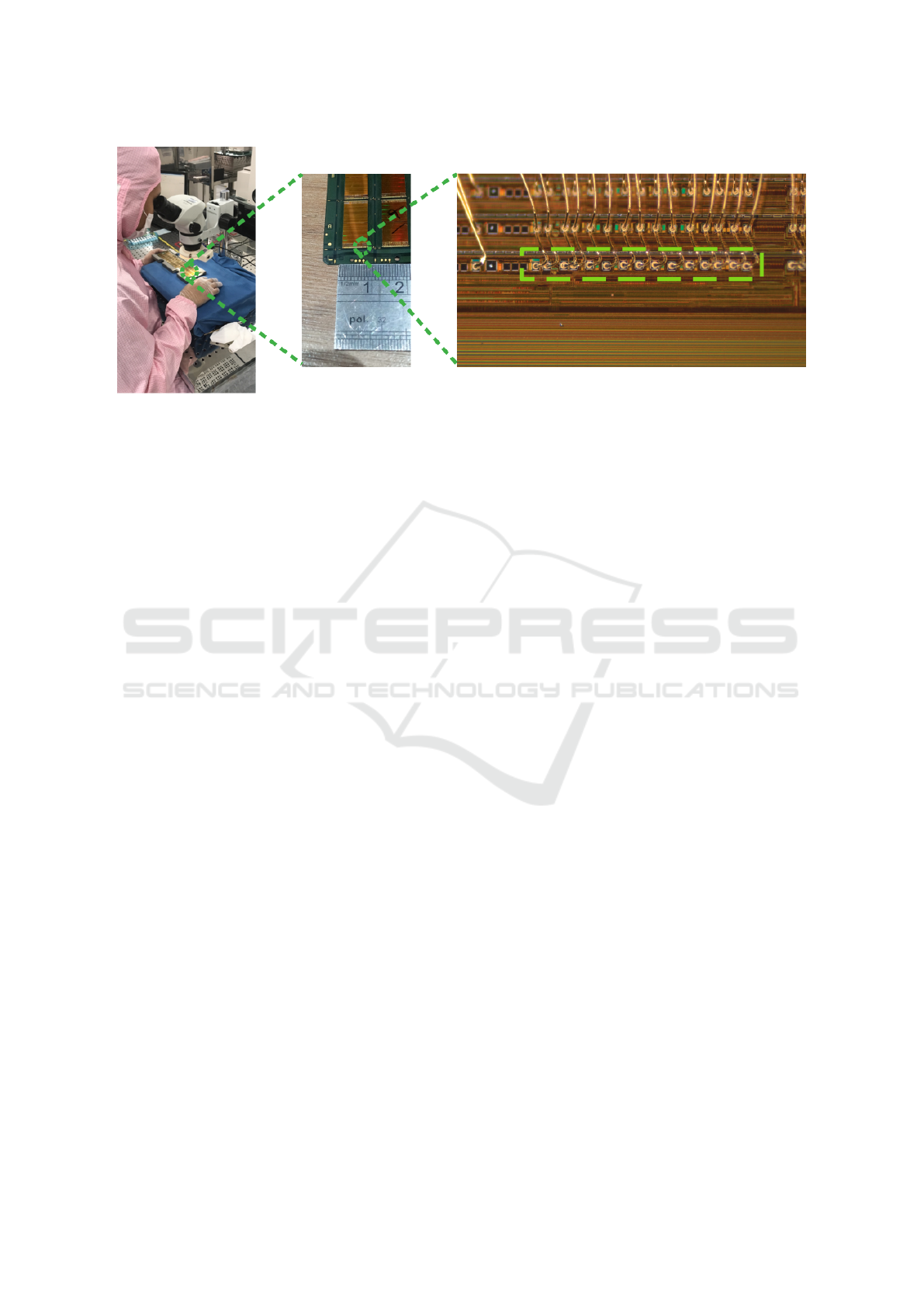
Figure 1: Conventional visual inspection of memory devices, in soldering process of silicon wafers. Additionally, are con-
trasted the sizes of a die and solder balls.
lations show that the obtained results are accurate and
applicable in industrial scenarios.
Our main contribution is to provide an approach,
based on deep learning, to detect failures in the die
soldering process. Furthermore, the proposed strat-
egy provides a robust solution for a challenging com-
ponent, in micrometers scale. Also in Figure 1, it is
possible observe the challenging size of solder balls
and the involved features to depict the problem.
The remainder of this paper is structured as fol-
lows. In Section II we present a discussion on re-
lated works regarding Semiconductor Inspection. The
proposed methodology is presented in Section III and
validated by real and simulated experiments discussed
in Section IV. Finally, in Section V we draw the con-
clusions and discuss paths for future investigation.
2 RELATED WORKS
Problems related to automatic visual inspection are of
significant importance and have been the subject of
intensive investigation (Huang et al., 2014) (Vafeiadis
et al., 2018)(Zhang et al., 2022). For fault detection,
the majority of works perform classification of pres-
ence or absence of faults, in manufacturing processes
(Rocha et al., 2016) (Zhang et al., 2021).
Many industrial applications are addressed as a
fault detection approach. In (Rocha et al., 2016), a
visual inspection approach is presented to detect ab-
sence/presence of surface mount components (SMC)
on printed circuit boards (PCB). The authors propose
a methodology based on the combination of Machine
Vision and Machine Learning (using Support Vector
Machine (SVM)) to detect component absence, with
more quality and precision, using noisy digital images
acquired directly from PCB industrial production line.
The obtained results demonstrated the robustness of
the methodology, obtaining 97.25% of accuracy.
(Zhou et al., 2017) has proposed a detection ap-
proach for oil-air and oil-water interfaces, from im-
ages of transparent tubes containing water and oil. A
statistical based approach to detect the mentioned in-
terfaces is used. Through real experiments, results
show that the multi-interface detection method has
high precision and reaches the requirements of indus-
trial applications.
In some industrial applications, semiconductor in-
spection is a paramount task. (Srivastava et al.,
2016) presents an inspection approach for patterned
wafer during the chip fabrication. The authors pro-
posed an unique combination of Broad-Band light
with Dark Field Apertures, to reduce potential defects
in manufacturing process. From the experiments, the
proposed inspection approach demonstrates effective-
ness in real application, achieving approximately 15
wafers per hour.
The authors of (Cao, 2021) proposed a robot vi-
sion inspection system. The industrial robot is used to
detect the surface defects of semiconductor metal tar-
gets online. In this paper, the main goal is to complete
a high purity semiconductor metal target processing
inspection task. As result, the system can completely
replace the traditional manual testing, and improve
the machining quality and efficiency of semiconduc-
tor metal target.
In (Zhou et al., 2021) is presented an approach
to inspect the chips in the wafer backside, during the
manufacturing process. In semiconductor analysis the
scan result is evaluated and compared to the Backside
Database (BDB), to quantify the accuracy achieved.
The experiments demonstrate the effectiveness of the
proposed approach for backside defect Monitoring
strategy.
The Visual Inspection of Solder Balls in Semiconductor Encapsulation
751
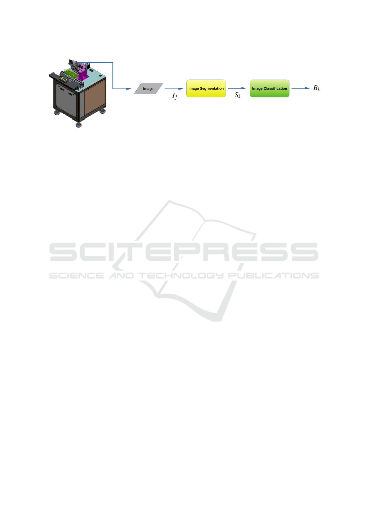
Figure 2: Overview of the proposed approach for automatic visual inspection for silicon wafer soldering process, through the
stages: i) Image Segmentation; and ii) Image Classification through deep learning.
Still in semiconductor inspection context, but re-
garding the soldering process, (Zhang et al., 2021)
proposed a strategy to inspect internal circuit boards
in the production of water pumps. In this paper the
authors design a solder joint inspection system based
on machine vision, which can detect the status of sol-
der joints and feed back the current soldering results
to the workers. The method solves the problem of
automatically detecting the welding quality of the cir-
cuit board in the manual welding process, greatly im-
proves the production efficiency of the workshop pro-
duction line, and shortens the product manufacturing
cycle.
(Chang et al., 2018) has proposed an inspection
technique for automated optical inspection (AOI) and
solder paste inspection (SPI), in SMT line. The au-
thors used a machine learning based approach called
automatic mistake reduction (AMR) for Classification
of solder joints in production line. The experimental
results showed that the proposed method is not only
more efficient, but also provides an accurate recogni-
tion rate in the SMT process.
In (Zhang et al., 2022) is proposed an approach
for solder joint defect detection on industrial manu-
facturing process. For this, the authors used a deep
learning based technique to learn features and detect
the failures through a CNN model. Through the ex-
periments the effectiveness of the proposed models is
verified by real-world 3D X-ray images.
The majority of the existing solutions for solder
evaluation are based on the classification of the solder
conditions on positive or negative cases (Chang et al.,
2018). The closest approach, regarding the method-
ological strategy, using CNN models, inspect solder
joints from x-ray images (Zhang et al., 2022). Addi-
tionally, the soldering process assessed by the major-
ity of works tackle milimiters and centimeters scales.
The presented approach is particularly interesting
because it proposes an automatic solder ball classi-
fication for PCB production. Additionally, it is im-
portant to mention that unlike other works whose
tackle solder conditions in millimeters and centime-
ters scale, our work tackle solder balls in micrometers
scale, representing a great challenge for an accurate
automatic visual inspection in semiconductor encap-
sulation process.
3 METHODOLOGY
In this paper, we propose an automatic visual inspec-
tion for silicon wafer soldering process, based on vi-
sual features and deep learning combining. The pro-
posed approach tackles the solder ball classification
problem, during the silicon wafer soldering process,
detecting failures in the semiconductor encapsulation
stage. An overview of the proposed methodology is
shown in Figure 2, whose details will be presented in
the next subsections.
In Figure 2, we present an overview of the
proposed approach, highlighting the main steps to
achieve the solder ball classification, indicating the
correct, absent or failure condition in the ball solder-
ing stage. To reach this goal, images are acquired
continuously and an image segmentation stage is per-
formed. Different features are learnt in a deep learn-
ing procedure, understanding the solder conditions
for an efficient classification.
Our problem can be summarized as follows:
Problem 1 (Automatic Visual Inspection). Let I =
{
i
1
, i
2
, . . . , i
n
}
be a series of silicon wafer images pro-
vided by a camera. For every i
j
∈ I , is extracted a set
of segmented solder ball images S
j
=
{
s
1
, s
2
, . . . , s
m
}
.
Also let B =
{
b
1
, b
2
, . . . , b
k
}
be a series of previously
known solder ball labels. Our main goal is to cor-
rectly associate an unknown segmented solder ball
image (s
w
) to the correspondent solder ball label (b
l
),
representing the solder ball condition during the sol-
dering process.
ICINCO 2022 - 19th International Conference on Informatics in Control, Automation and Robotics
752
3.1 Image Segmentation
In this work the images (I) are initially acquired in
Red, Green and Blue (RGB) model. The first step to
inspect the soldering stage, during the semiconductor
encapsulation process, is to segment the solder balls
(S) contained in the silicon wafer images.
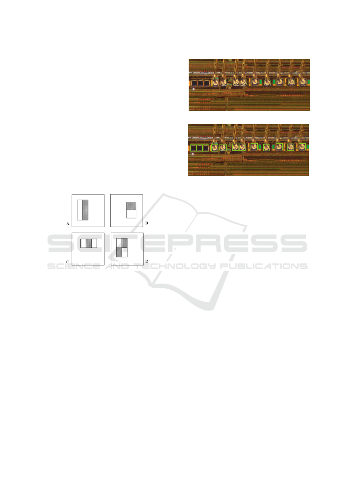
For this solder ball segmentation step, the Haar
cascade method, using boosted cascade of simple fea-
tures, is used (Viola and Jones, 2001). The Haar cas-
cade method works like a machine learning approach,
where the cascade function is trained from a set of
images representing positive and negative cases.
In Haar cascade, for solder ball detection, rectan-
gle features are used to learn patterns. For this, the
sum of the pixels which lie within the white rectan-
gles are subtracted from the sum of pixels in the grey
rectangles. Some rectangle features are shown in Fig-
ure 3.
Figure 3: Examples of rectangle features used in Haar cas-
cade method for solder ball detection in silicon wafer im-
ages.
For the learning process a variant of Ada Boosting
is used both to select a small set of features and train a
classifier (Viola and Jones, 2001). Ada Boosting is an
algorithm used to boost the classification performance
of weak classifiers. Additionally, is designed to select
the single rectangle feature which best separates the
positive and negative examples. For each feature, the
weak learner determines the optimal threshold classi-
fication function, such that the minimum number of
examples are misclassified.
A weak classifier h
j
(x) thus consists of a feature
f
j
, a threshold θ
j
, and a polarity p
j
indicating the di-
rection of the inequality sign:
h
j
(x) =
(
1 if p
j
f
j
(x) < p
j
θ
j
0 otherwise
(1)
Where x is a 24x24 pixel sub-window of an image.
Figure 4 shows the process of solder ball detection
using Haar cascade objetct detection.
(a)
(b)
Figure 4: Example of solder ball detection using Haar cas-
cade method. Figure 4a corresponds to raw silicon wafer
image. Figure 4b corresponds to the solder ball region de-
tection.
3.2 Image Classification
From the segmented solder ball images (S), is per-
formed a classification process to identify different
solder ball conditions (B), like: i) correct; ii) absence;
or iii) failure. For this, in this work, is proposed a
deep learning based approach to understand patterns
and features in different soldering cases.
A CNN is a deep learning architecture strongly
used for computer vision applications. CNN mod-
els can learn and represent effective features to al-
low the classification or regression application in real
problems. In solder ball classification context the pro-
posed CNN model, unlike other classical approaches,
can learns the better features and its representation for
the classification stage, even in different scenarios and
domains.
The proposed CNN model is composed by two
convolutional layers, with 16 filters in first layer and
32 filters in second layer. The filters size in first
layer were (5, 5), while in second layer were (9, 9).
The size of the fully-connected layer were 100. The
ReLU activation function is used in convolutional lay-
ers, with Max Pooling of size window (2, 2). In the
training stage, are used: the SGD optimization algo-
rithm, learning rate equals to 0.001, with momentum
0.9; for 40 epochs and using a batch size of 32.
A CNN model is used for solder ball classifica-
tion due to good results achieved in semiconductor
automation scenarios (Zhang et al., 2022). The pro-
posed CNN model is also used due to good feature
representation learning, depicting distinct and com-
The Visual Inspection of Solder Balls in Semiconductor Encapsulation
753
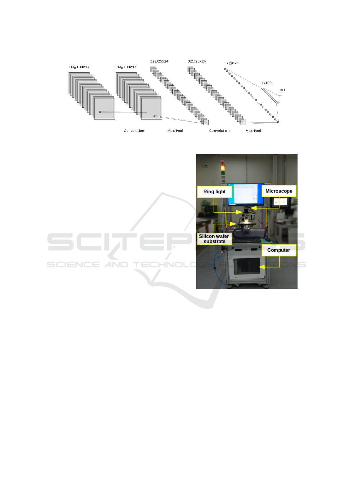
Figure 5: Proposed CNN architecture.
plementary features for modeling of different solder
ball conditions, unlike classical approaches. The pro-
posed CNN architecture for the soldering stage, dur-
ing the semiconductor encapsulation process, can be
observed in Figure 5.
4 EXPERIMENTS
In this section we present experimental results and
compare the obtained performance against existing
approaches.
4.1 Experimental Setup
The proposed experimental setup is composed by an
Olympus stereomicroscope SZ61-TR, coupled with a
camera SC180, mounted on a XYZ cartesian robot
with precise movements. Additionally, a ring light
is coupled with the stereomicroscope, providing con-
trolled illumination conditions. A Dell computer with
an Intel
®
Core
T M
i7-8550U CPU and 32 GiB DDR3-
2133 main memory is used to execute the proposed
approach (Figure 6).
4.2 Solder Ball Classification
Assessment
This experiment evaluates the accuracy of the pro-
posed approach for solder ball classification. Dif-
ferent approaches to tackle the solder ball classifica-
tion problem are implemented and evaluated. The
comparison approaches are: i) Local Binary Pattern
(LBP) and SVM classifier, with third degree polyno-
mial kernel; ii) LBP and Ada Boosting (AB) clas-
sifier; iii) LBP and Random Forest (RF) classifier;
iv) Histogram of Oriented Gradient (HOG) and SVM
classifier, with third degree polynomial kernel; v)
HOG and AB classifier; and vi) HOG and RF clas-
sifier. The comparison techniques were used due
Figure 6: Experimental setup used for automatic visual in-
spection for solder balls in PCB manufacturing process.
to good results obtained in automatic semiconductor
analysis (Iglesias. et al., 2021) and overall automatic
visual inspection context (Rahman et al., 2019)(Thie-
len et al., 2020).
The setting parameters for SVM classifier, with
polynomial kernel, were gamma equals to 0.001, C
equals to 1.0 and kernel degree equals to 3. For AB
classifier the setting parameters were, number of esti-
mators equals to 100. For RF classifier the setting pa-
rameters were, number of estimators equals to 30 and
max depth equals to 30. The parameters tuning for
the proposed approach was performed varying a set
of parameters to maximize accuracy, during the train-
ing and testing stages. Different scenarios changing
the number of convolutional layers, the number of fil-
ters, the size of filters, the number of fully-connected
layers, the size of the fully-connected layers and the
ICINCO 2022 - 19th International Conference on Informatics in Control, Automation and Robotics
754
learning rate were experimented.
The classification model training is performed
from a set of input images and the testing stage re-
gards another set of input images, since is applied the
cross validation 5-fold protocol. The dataset used for
the training process, is composed by 1003 images of
solder balls, acquired during the semiconductor en-
capsulation process
The achieved results show that the proposed CNN
model outperforms the other classic techniques, as we
can observe in Table 1. The better classic perfor-
mances were obtained using LBP descriptor, depict-
ing texture features, and HOG descriptor, depicting
shape features. In addition, were used the RF classi-
fier to detect failures during the soldering stage.
Table 1: Results for solder ball classification. This experi-
ment presents the accuracy for CNN (proposed), HOG and
LBP descriptors. Additionally, were used the Random For-
est (RF), Support Vector Machine (SVM-Poly3) and Ada
Boosting (AB) for classification problem.
Method Accuracy
LBP + SVM Poly 3 26.208 ± 3.345
LBP + AB 84.345 ± 2.937
LBP + RF 90.627 ± 0.975
HOG + SVM Poly 3 19.342 ± 3.076
HOG + AB 87.241 ± 2.088
HOG + RF 95.114 ± 0.736
Our method 99.400 ± 0.583
The proposed approach achieved accurate results,
in the solder ball classification process, due to the
learning of different filters during soldering process.
The CNN process allows the learning of patterns in
different contexts and regarding different features.
Thereby, some solder ball conditions can be bet-
ter represented and classified using the convolutional
learning process.
4.3 Robustness Evaluation of Solder
Ball Classification in Presence of
Noise
This experiment evaluates the robustness of the pro-
posed approach for solder ball classification in pres-
ence of noise. Two different types of noise are added
in solder ball images, Salt and Pepper and Gaussian
noises. All the classic techniques, used in experiment
4.2 and the proposed CNN model, are evaluated. In
this experiment the added noise simulates the image
acquisition process regarding the presence of noise.
For this assessment, the classification model train-
ing is performed from a set of images without noise
and the testing stage regards another set of images
Table 2: Results for robustness evaluation of solder ball
classification, in presence of noise. In this experiment all
the considered methods are evaluated for Salt and Pepper
noise.
Salt and Pepper
Noise density 0.005 0.01 0.02
LBP+SVM
19.342
± 3.076
19.342
± 3.076
19.342
± 3.076
LBP+AB
83.944
± 2.579
82.450
± 2.361
75.664
± 6.442
LBP+RF
90.127
± 1.214
90.025
± 2.094
87.134
± 2.060
HOG+SVM
19.342
± 3.076
19.342
± 3.076
19.342
± 3.076
HOG+AB
76.663
± 3.336
60.505
± 7.125
27.508
± 5.172
HOG+RF
83.452
± 2.376
74.076
± 2.700
37.082
± 4.371
Our method
97.163
± 0.707
95.275
± 1.030
92.846
± 3.836
Table 3: Results for robustness evaluation of solder ball
classification, in presence of noise. In this experiment all
the considered methods are evaluated for Gaussian noise.
Gaussian
Noise density 0.005 0.01 0.02
LBP+SVM
19.342
± 3.076
19.342
± 3.076
19.342
± 3.076
LBP+AB
17.948
± 2.031
17.748
± 3.463
18.147
± 2.459
LBP+RF
19.342
± 3.076
19.242
± 3.029
19.142
± 2.994
HOG+SVM
19.342
± 3.076
19.342
± 3.076
19.342
± 3.076
HOG+AB
15.548
± 2.271
15.655
± 1.455
15.951
± 2.014
HOG+RF
24.025
± 5.277
20.240
± 4.440
16.155
± 1.634
Our method
81.602
± 1.748
79.430
± 2.916
75.703
± 3.175
with added noise. Figure 7 represents solder ball im-
age examples. Figure 7a represents a solder ball with-
out noise. Figure 7b represents a solder ball with Salt
and Pepper noise, with 0.02 noise density. Figure 7c
represents a solder ball with Gaussian noise, with 0.02
noise density.
The achieved results in this experiment show that
the proposed CNN model presents better performance
even in the presence of noise, as we can observe in
Table 2 and Table 3. Table 2, through the accuracy
and variance measures, shows the solder ball classi-
fication results for Salt and Pepper noise, for the dif-
ferent used techniques. Table 3, through the accuracy
The Visual Inspection of Solder Balls in Semiconductor Encapsulation
755
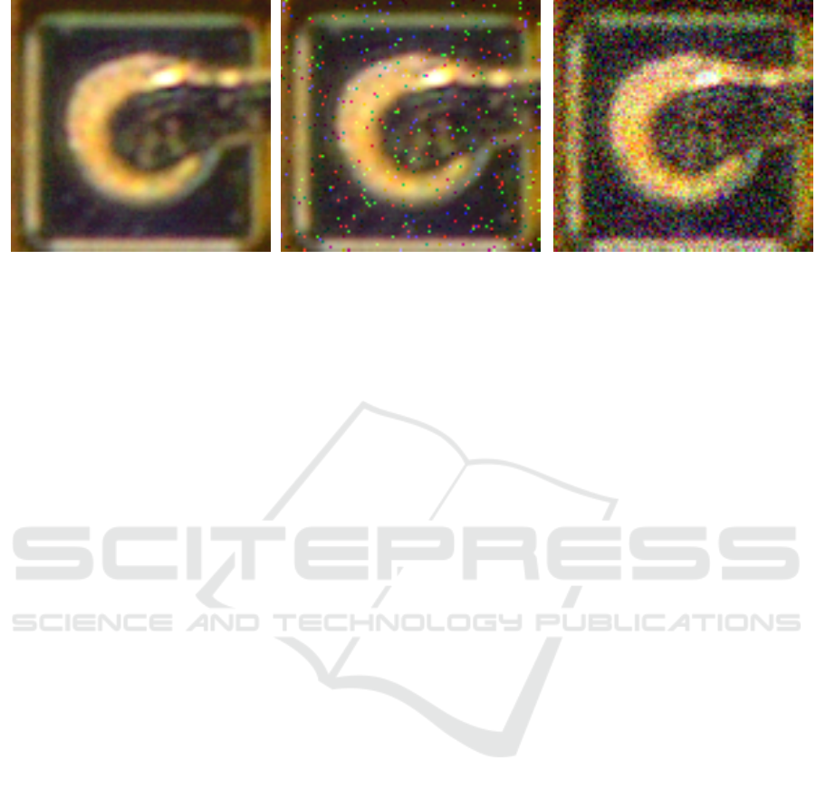
(a) (b) (c)
Figure 7: Example of solder ball images in presence of noise. Figure 7a corresponds to raw solder ball image. Figures 7b and
7c correspond to raw image added with Salt and Pepper noise and Gaussian noise, respectively.
and variance measures, shows the solder ball classi-
fication results for Gaussian noise, for the different
used techniques. Results show that the proposed CNN
model outperforms the other classification approaches
even in presence of noise, demonstrating the robust-
ness of the proposed approach.
5 CONCLUSION
In this paper, we addressed the problem of solder-
ing visual inspection in semiconductor encapsulation.
Unlike other state-of-the-art approaches, our method
achieve high accuracy and present the great capacity
of inspect very tiny solder ball conditions, providing
improvement to the semiconductor encapsulation and
production process.
Real-world and simulated experiments involving
different classification techniques and simulated noise
types have shown that the obtained solder ball clas-
sifications are reliable and accurate, considering the
obtained results. Additionally, the proposed approach
demonstrates robustness, even in presence of noise
during image acquisition, and feasibility to real indus-
trial application, once the experiments were carried
out in real scenario.
As future work, we intend to combine different
classification methods to improve the solder ball clas-
sification accuracy. We also intend to concentrate
efforts to extend the automatic visual inspection ap-
proach to tackle other types of problems related to
semiconductor encapsulation. The wire bond analysis
and inspection is also a relevant problem we intend to
investigate and incorporate in production lines.
ACKNOWLEDGMENT
This work was developed with support from Cal-
Comp Eletronic through R&D project in Institute of
Exact Sciences and Technology of Federal University
of Amazonas, Itacoatiara, Amazonas.
REFERENCES
Cao, Y. (2021). Design and application of robot vision in-
spection system for semiconductor metal target. In
2021 3rd International Symposium on Robotics In-
telligent Manufacturing Technology (ISRIMT), pages
464–467.
Chang, Y.-M., Wei, C.-C., Chen, J., and Hsieh, P. (2018).
Classification of solder joints via automatic mistake
reduction system for improvement of aoi inspection.
In 2018 13th International Microsystems, Packaging,
Assembly and Circuits Technology Conference (IM-
PACT), pages 150–153.
Huang, R., Sorini, A., and McNulty, J. (2014). Quantita-
tive solder inspection with computed tomography. In
2014 IEEE Symposium on Product Compliance Engi-
neering (ISPCE), pages 82–85.
Iglesias., B., Otani., M., and Oliveira., F. (2021). Glue
level estimation through automatic visual inspection
in pcb manufacturing. In Proceedings of the 18th
International Conference on Informatics in Control,
Automation and Robotics - ICINCO,, pages 731–738.
INSTICC, SciTePress.
Rahman, N. N. S. A., Saad, N. M., Abdullah, A. R., and
Ahmat, N. (2019). A REVIEW OF VISION BASED
DEFECT DETECTION USING IMAGE PROCESS-
ING TECHNIQUES FOR BEVERAGE MANUFAC-
TURING INDUSTRY. Jurnal Teknologi, 81(3).
Rocha, C. S., Menezes, M. A. G., and Oliveira, F. G.
(2016). Detecc¸
˜
ao autom
´
atica de microcomponentes
smt ausentes em placas de circuito impresso. In
ICINCO 2022 - 19th International Conference on Informatics in Control, Automation and Robotics
756

Menotti, D. and Miranda, P., editors, Workshop on In-
dustry Applications (WIA) in the 29th Conference on
Graphics, Patterns and Images (SIBGRAPI’16), vol-
ume 1, S
˜
ao Jos
´
e dos Campos, SP, Brazil.
Srivastava, A., Tolle, I., Mraz, A., Gupta, S., Huang, R.,
Nguyen, H., Dey, L., Jain, A., Lee, S.-H., and Kini, S.
(2016). Non-traditional inspection strategy for inline
monitoring in excursion scenarios: Defect inspection.
In 2016 27th Annual SEMI Advanced Semiconductor
Manufacturing Conference (ASMC), pages 197–200.
Thielen, N., Werner, D., Schmidt, K., Seidel, R., Reinhardt,
A., and Franke, J. (2020). A machine learning based
approach to detect false calls in smt manufacturing. In
2020 43rd International Spring Seminar on Electron-
ics Technology (ISSE), pages 1–6.
Vafeiadis, T., Dimitriou, N., Ioannidis, D., Wotherspoon, T.,
Tinker, G., and Tzovaras, D. (2018). A framework for
inspection of dies attachment on PCB utilizing ma-
chine learning techniques. Journal of Management
Analytics, 5(2):81–94.
Viola, P. and Jones, M. (2001). Rapid object detection us-
ing a boosted cascade of simple features. In Proceed-
ings of the 2001 IEEE Computer Society Conference
on Computer Vision and Pattern Recognition. CVPR
2001, volume 1, pages I–I.
Zhang, K., Huang, T., Su, Z., and Guan, T. (2021). De-
sign of solder quality inspection system based on ma-
chine vision. In 2021 IEEE 5th Advanced Information
Technology, Electronic and Automation Control Con-
ference (IAEAC), volume 5, pages 2413–2418.
Zhang, Q., Zhang, M., Gamanayake, C., Yuen, C., Geng,
Z., Jayasekara, H., wei Woo, C., Low, J., Liu, X.,
and Guan, Y. L. (2022). Deep learning based sol-
der joint defect detection on industrial printed circuit
board x-ray images. Complex & Intelligent Systems,
8(2):1525–1537.
Zhou, D., Zhang, G., and Guo, Y. (2017). Detecting multi-
interface from oil-water separation image based on
difference statistics method. In 2017 IEEE Inter-
national Conference on Smart Cloud (SmartCloud).
IEEE.
Zhou, J. G., Chen, H., Long, Y., Wang, K., Guo, H., and
Liu, F. (2021). Backside defect monitoring strat-
egy and improvement in the advanced semiconductor
manufacturing. In 2021 China Semiconductor Tech-
nology International Conference (CSTIC), pages 1–5.
The Visual Inspection of Solder Balls in Semiconductor Encapsulation
757
