
A New Architecture Proposal of Half-wave Precision Rectifier using a
Single VCII
Leila Safari
1,2 a
, Gianluca Barile
1,2 b
, Mattia Ragnoli
1 c
, Giuseppe Ferri
1 d
and Vincenzo Stornelli
1,2 e
1
Department of Industrial and Information Engineering, University of L’Aquila, Italy Località Campo di Pile,
via Gronchi 18, L’Aquila 67100, Italy
2
DEWS research center, University of L’Aquila, Italy Località Campo di Pile, via Gronchi 18, L’Aquila 67100, Italy
vincenzo.stornelli}@univaq.it
Keywords: Current Mode, Current Conveyor, Half Wave Rectifier, VCII, Signal Conditioning, Sensors, Voltage
Conveyor.
Abstract: In this paper a new second generation voltage conveyor (VCII) based half wave rectifier circuit architecture
proposal is presented. Both inverting and non-inverting outputs in the form of voltage signal are produced.
The proposed circuit is the first half wave rectifier architecture using VCIIs introduced in the literature. It
consists of one VCII, two diodes and a single grounded resistor. The input signal is in current form and the
rectified output voltage signal is provided at the low impedance Z port of the same VCII. Therefore, the
produced output signal can be directly used with no need to add extra voltage buffers. In addition, the circuit
gain is set by the grounded resistor value and can be tuned. The proposed circuit enjoys a simple transistor-
level structure employing only 21 transistors. In this paper, the architecture of the rectifier is presented and
explained, as well as a possible VCII topology. Preliminary simulation results are also given highlighting its
capabilities. Its simplicity and versatility make it suitable for sensor interfaces and processing circuits for
sensor networks where a low power consumption for the analog processing section is of the utmost
importance.
1 INTRODUCTION
Circuits converting alternating signals to direct
signals are basic building blocks used in various
signal processing fields such as applications
requiring RMS to DC conversion, AC voltmeters,
low level signal conditioning, measurement,
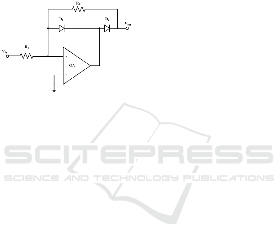
instrumentation etc. (Toumazou et al., 1987). Figure
1 shows the traditional operational amplifier (OA)
based half wave precision rectifier realization
(Samyhosny et al., 1994). There are two main
advantages for the circuit of Fig.1.
First, the rectified output signal can be directly
used because the rectified output is provided in the
form of voltage signal at low impedance output port
a
https://orcid.org/0000-0003-0863-5660
b
https://orcid.org/0000-0003-4937-0398
c
https://orcid.org/0000-0002-1536-3969
d
https://orcid.org/0000-0002-8060-9558
e
https://orcid.org/0000-0001-7082-9429
of OA. Second, OA also reduces the problem of
diode cut-in voltage. However, the conventional OA
based half wave rectifier of Fig.1 is limited to operate
well below OA gain bandwidth product (GBW) and
hence it is not suitable for high frequency
applications. More importantly, there is large
distortion in the output signal in zero crossing due to
the finite slew rate of OA. The problems associated
with conventional OA based rectifier is effectively
solved using current mode approach. Several
precision rectifiers based on current mode active
building blocks have been reported in open literature
(Kumngern, 2009; Virattiya et al., 2011; Kumngern,
2010; Monpapassorn et al., 2001; Oruganti et al.,
2017; Lidgey et al. 1993; Kumar et al.; 2020; Sagbas
158
Safari, L., Barile, G., Ragnoli, M., Ferri, G. and Stornelli, V.
A New Architecture Proposal of Half-wave Precision Rectifier using a Single VCII.
DOI: 10.5220/0010901900003118
In Proceedings of the 11th International Conference on Sensor Networks (SENSORNETS 2022), pages 158-162
ISBN: 978-989-758-551-7; ISSN: 2184-4380
Copyright
c
2022 by SCITEPRESS – Science and Technology Publications, Lda. All rights reserved
et al; 2016; Hirunporm et al.; 2021). The possibility
of driving diodes by high output impedance current
sources which eliminates the problems caused by
limited slew rate of OAs as well as inherent high
frequency
Figure 1: OA based half wave rectifier (Samyhosny et al.,
1994).
performance of current mode active building block
are two main motivations in realizing various current
mode precision rectifiers.
Literature survey shows that current mode signal
processing has been helpful in overcoming the issues
related to OA based precision rectifiers. However,
current mode precision rectifiers suffer from a great
weakness in applications where rectified output
signal is required in voltage form. This is mainly
because most of current mode active building blocks
lacks a low impedance voltage output port. For
example, in (Kumngern, 2009) a voltage output half
wave rectifier is presented. It employs a voltage to
current converter and 21 MOS transistors. The circuit
requires extra voltage buffer at output for practical
use. In (Virattiya et al., 2011) a half-wave rectifier
using a current comparator and two current mirrors is
presented. The output signal is in the form of current.
The half-wave rectifier reported in (Kumngern, 2010)
employs an operational trans-resistance amplifier
(OTA), two diodes, one reference voltage and one
grounded resistor. The half-wave rectifier of
(Monpapassorn et al., 2001) employs an I-V
converter, half wave rectifier, and a V-I converter. In
(Oruganti et al., 2017) a voltage output half-wave
rectifier based on two OTA, five resistors, one bias
voltage and 6 MOS transistors is reported. However,
all the aforementioned solutions suffer from
inappropriate impedance at output node and for
practical use, voltage buffer is required.
Recently, a new active building block called
second generation voltage conveyor (VCII) (Safari et
al., 2019a, 2019b) that shows a low impedance
voltage output port, has gained great interest for
applications requiring voltage signals. Literature
study shows that VCII can be used in many
applications such as: analog interface circuit for
capacitive sensors (Barile et al., 2019a), SiPM
interface circuit (Ferri et al., 2021), instrumentation
(Safari et al., 2021), multiplying circuit for low value
capacitive sensors (Stornelli et al., 2021) etc. More
importantly, VCII application as a voltage output full
wave precision rectifier has been reported recently
(Safari et al., 2020). In this paper we propose a new
architecture for VCII based voltage output half wave
precision rectifier implementation. The proposed
topology employs only one VCII, two diodes and one
grounded resistor. Both inverting and non-inverting
outputs can be provided at low impedance Z port of
VCII. The overall gain can be simply set by resistor
value. The organization of this paper is as follows: in
section 2 proposed circuit architecture is discussed.
Section 3 describes the transistor level architecture of
the implemented VCII. Lastly, section 4 draws some
conclusions.
2 PROPOSED ARCHITECTURES
Figure 1 shows the VCII symbol and the internal
structure. As it is shown, it consists of a current buffer
and a voltage buffer. Y is low impedance current
input port, X is high impedance current output port
and Z is low impedance voltage output port. The
operation of VCII is described as:
(1)
where β is current gain between Y and X terminals
and α is voltage gain between X and Z terminals. The
ideal values of β and α are unity. The + and – signs
indicate VCII+ and VCII- respectively. The parasitic
impedances at Y, X and Z terminals (r
Y
, r
X
and r
Z
respectively) in ideal case are zero, infinite and zero
respectively. The proposed VCII- based half wave
positive and negative rectifiers are shown in Fig.3a
and Fig.3b respectively
A New Architecture Proposal of Half-wave Precision Rectifier using a Single VCII
159
(a)
(b)
Figure 2: The VCII: a) schematic diagram b) symbolic
representation (Safari et al., 2019a).
They are based on two diodes, one grounded
resistor and one VCII- as active element. The input
signal is in current form and the produced rectified
output signal is in voltage form. For Fig.3a, by
ignoring parasitic impedances, its operation can be
described as follows: for I
in
> 0, D
1
is off and D
2
is on,
and we have:
(2)
From eq.(1), we have:
(3)
Using eq.(3) and eq.(1), V
out
is found as:
(4)
For I
in
< 0, D
1
is on and D
2
is off, and we have:
(5)
Therefore, the operation of the proposed positive
VCII- based half wave rectifier can be expressed as:
(6)
As it is seen from eq.(6), the circuit gain can be
set by R
1
value.
The proposed negative half wave rectifier is shown in
Fig.3b. Similarly, its operation is expressed as:
(7)
(a)
(b)
Figure 3: Proposed a) positive and b) negative half wave
rectifiers.
(a)
(b)
Figure 4: Time domain analysis of the a) positive and b)
negative half wave rectifiers.
SENSORNETS 2022 - 11th International Conference on Sensor Networks
160
Figure 4 shows an example of time domain
behavior of the positive (Fig.4a) and negative
(Fig.4b) rectifiers. The VCII topology used for these
simulations is reported in Section 4, while the used
diodes are 1PS79SB63 (Datasheet 1PS79SB63,
2004). The input signal is a sinusoidal wave with an
amplitude of 10 µA and a frequency of 10 kHz. The
output voltage is reported at different values of R
1
: 1
kΩ, 10 kΩ, 20 kΩ and 40 kΩ.
3 VCII INTERNAL TOPOLOGY
The CMOS implementation of the VCII- is shown in
Fig.5. A current buffer made of transistors M
1
-M
9
transfer Y port input current to X node. The voltage
produced at X node is conveyed to Z port by means
of a voltage buffer realized by M
10
-M
14
. Transistors
M
B1
-M
B6
are used for biasing purpose.
The circuit was designed using AMS 0.35 µm
technology, with a ±1.65 V supply voltage. The total
power consumption is 600 µW.
Simulation results concerning the main VCII
parameters are reported in Fig. 6 and Fig. 7.
Specifically, Fig. 6 shows the two parameters α and
β, where the value is equal to 0.995 and 0.975
respectively. Terminal impedances are shown in Fig.
7: at X node the high impedance equals 1.65 MΩ,
whereas at the low impedance nodes Y and Z there
are 50 Ω and 87 Ω, respectively
Figure 6: VCII
-
α and β parameters.
Figure 7: VCII
-
impedances.
Figure 5: CMOS implementation of VCII
-
.
A New Architecture Proposal of Half-wave Precision Rectifier using a Single VCII
161

4 CONCLUSIONS
A new circuit topology for realizing inverting and
non-inverting half wave rectifiers is presented. Only
one VCII-, two diodes and a single resistor are used.
The circuit gain can be adjusted by resistor value. The
input signal is in current form and rectified output
signal is in voltage form which is provided in low
impedance Z port of VCII
-
. Therefore, no voltage
buffer is required for practical application. Simple
implementation, high frequency performance, low
power consumption and low linearity error are main
advantages of the proposed half wave rectifier
topology.
ACKNOWLEDGEMENTS
This research has been partially founded by the
European co-funded innovation project iRel4.0
ECSEL under grant agreement No 876659.
REFERENCES
Toumazou C., Lidgey F. (1987). Wide-Band precision
rectification. IEE Proceedings G (Electronic Circuits
And Systems). 134 - 7. doi:10.1049/ip-g-1.1987.0002.
Samyhosny M., Hanson J. (1994). A Wide-Band, High-
Precision CMOS Rectifier. Analog Integrated Circuits
and Signal Processing 5, 183-190.
Kumngern M.(2009). A wide-band half-wave rectifier.
Proceedings of the 2009 12th International Symposium
on Integrated Circuits, 2009, pp. 498-501.
Virattiya A., Knobnob B., Kumngern M. (2011). CMOS
precision full-wave and half-wave rectifier. IEEE
International Conference on Computer Science and
Automation Engineering, pp. 556-559, doi:
10.1109/CSAE.2011.5952911.
Kumngern M. (2010). High frequency and high precision
CMOS full-wave rectifier. IEEE International
Conference on Communication Systems, pp. 5-8, doi:
10.1109/ICCS.2010.5686166.
Monpapassorn A., Dejhan K., Cheevasuvit F. (2001).
CMOS dual output current mode half-wave rectifier.
International Journal of Electronics, vol. 88, pp. 1073–
1084.
Oruganti S., Gilhotra Y., Pandey N., Pandey R. (2017).
New topologies for OTRA based programmable
precision half-wave and full-wave rectifiers. Recent
Developments in Control, Automation & Power
Engineering (RDCAPE), pp. 327-331,
doi:10.1109/RDCAPE.2017.8358291.
Lidgey F.J., Hayatleh K., Toumazou C. (1993). New
current-mode precision rectifiers. IEEE International
Symposium on Circuits and Systems, 1993, pp. 1322-
1325 vol.2, doi: 10.1109/ISCAS.1993.393974.
Kumar A., Chaturvedi B. (2020). Current-Mode MOS Only
Precision Full-Wave Rectifier. IETE Journal of
Research, DOI: 10.1080/03772063.2020.1830861.
Sagbas M., Minaei S., Engin Ayten E. (2016). Component
reduced current-mode full-wave rectifier circuits using
single active component. IET Circuits Devices Syst., p.
1–11.
Hirunporm J., Saksiri W., Siripruchyanun M. (2021).
Electronically Controllable Precision Rectifiers Based
on Voltage Differencing Gain Amplifier., 18th
International Conference on Electrical
Engineering/Electronics Computer
Telecommunications and Information Technology
(ECTI-CON), pp. 704-707.
Safari L., Barile G., Stornelli V., Ferri G. (2019). An
Overview on the Second Generation Voltage
Conveyor: Features, Design and Applications. IEEE
Transactions On Circuits And Systems II: Express
Briefs. 66 , 547-551. doi:10.1109/tcsii.2018.2868744.
Safari L., Barile G., Ferri G., Stornelli V. (2019).
Traditional Op-Amp and new VCII: A comparison on
analog circuits applications. AEU - International
Journal of Electronics and Communications. 110. doi:
10.1016/j.aeue.2019.152845.
Barile G., Safari L., Stornelli V., Ferri G. (2019). A VCII-
Based Stray Insensitive Analog Interface for
Differential Capacitance Sensors. Sensors, 19(16),
3545; https://doi.org/10.3390/s19163545.
Ferri G., Safari L., Barile G., Stornelli V. (2021). Noise
analysis and optimization of VCII-based SiPM
interface circuit. Analog Integrated Circuits and Signal
Processing, 109(3):1-9 DOI: 10.1007/s10470-020-
01745-3.
Safari L., Barile G., Stornelli V., Leoni A., Ferri G. (2018).
New Current Mode Wheatstone Bridge Topologies
with Intrinsic Linearity. 14th Conference on Ph.D.
Research in Microelectronics and Electronics
(PRIME), DOI: 10.1109/PRIME.2018.8430363
Stornelli V., Safari L., Barile G., Ferri G. (2020). A New
Extremely Low Power Temperature Insensitive
Electronically Tunable VCII Based Grounded
Capacitance Multiplier. Circuits and Systems II:
Express Briefs, IEEE Transactions on PP (99):1-1.
Safari L., Barile G., Stornelli V., Ferri G.(2020). A new
versatile full wave rectifier using voltage conveyors.
AEU – Int. J. Electron. Commun., Vol. 122, pp. 153267.
Datasheet 1PS79SB63, Philips Semiconductors, Rev. 02,
Dec 2004.
SENSORNETS 2022 - 11th International Conference on Sensor Networks
162
