
Native Ethernet Optical Switching for Deterministic
Critical Networks
Brice Leclerc, Olivier Marce, Bogdan Uscumlic and Dominique Chiaroni
Nokia Bell Labs France, Route de Villejust, 91620 Nozay, France
Keywords: Deterministic Networks, Native Ethernet, Optical Technologies, Optical Switching, Latency, Energy
Efficiency.
Abstract: In this paper we present a novel approach enabling the switching of native Ethernet frames directly in the
optical domain without any buffering. This is possible for the first time in the optical domain thanks to our
approach using the known Ethernet frames arrival times, to preconfigure the fast-optical switches to build a
new optical path before arrival of the Ethernet packet. The technique is analysed and validated with an
Ethernet frame analyser to demonstrate its feasibility.
1 INTRODUCTION
Time sensitive applications require new technologies
and approaches to make the latency as small as
possible. It was identified that deterministic switching
is a key for time sensitive applications (Barth,
Guiraud, Leclerc, Marcé and Strozecki, 2018).
However, to reach optimal performance, current
optical switching systems handling variable packets
have to add an additional insertion delay when
forming the optical packets prior to the traffic
transport in optics. Indeed, this step is necessary in
order to achieve a high bandwidth usage of the optical
resources. This trade-off in optics between the
bandwidth usage and the delay is highly punitive to
the time-sensitive traffic. The packet insertion
process requires additional buffers that introduces
latency and jitter.
In this paper we present a novel approach by
switching native Ethernet frames directly in the
optical domain without any buffering. This is possible
for the first time, to the best of our knowledge, in the
optical domain thanks to our approach using the
known Ethernet frame arrival times, to preconfigure
the fast optical switches to build a new optical path
before the arrival of the Ethernet frames. Indeed, for
the time-sensitive traffic the frames arrival times are
known in advance. This approach is made possible by
the following assumption: applications that require
low latency usually exhibit flows with temporal
regularity. This is for example the case in the
Industry 4.0 context where low latencies are required
for Machine To Machine Communications e.g.
repeatedly monitoring and signalling the status of the
work. Focusing on temporal patterns of such flows
opens the door to a new paradigm that we explore in
this paper.
Our focus in the present work is to show a proof
of concept of the proposed solution. For this purpose,
as an underlying optical transport technology we
adopt nanosecond range optical switches to maintain
the transmission efficiency at a high level (Chiaroni,
2017).
In this paper, section 2 will describe the context
and the use case considered. Section 3 will describe
the optical interconnection considered based on a
structure of an add/drop multiplexer already proposed
in (Argibay-Losada and Chiaroni, 2020) and its
simulated performance. In the same section we will
also describe the testbed of the proposed switch.
Section 4 will comment the performance obtained
demonstrating the Proof of Concept (PoC). Finally,
section 5 will draw a conclusion.
2 CONTEXT AND USE CASE
Time sensitive networks are more and more required
for some applications. In this paper we will then
address the case of a product line designed for the
Industry 4.0, requiring machine to machine
communications in a deterministic way. To support
42
Leclerc, B., Marce, O., Uscumlic, B. and Chiaroni, D.
Native Ethernet Optical Switching for Deterministic Critical Networks.
DOI: 10.5220/0010828800003121
In Proceedings of the 10th International Conference on Photonics, Optics and Laser Technology (PHOTOPTICS 2022), pages 42-47
ISBN: 978-989-758-554-8; ISSN: 2184-4364
Copyright
c
2022 by SCITEPRESS – Science and Technology Publications, Lda. All rights reserved
exchanges at high bit rates, to enable a machine to
machine cooperation, we propose here to analyse
optical ring networks operating at the packet
granularity for more network efficiency. For a
product line we assume the need to interact with up to
10 machines. So, we will adopt a technology that has
been validated for a cascade of 10 nodes, based on
Time Slotted Add/Drop Multiplexer structures. For
the validation of the native Ethernet switching
regime, we will adopt a testbed interconnecting 3
machines over the 10, requiring deterministic
communications.
3 OPTICAL RING NETWORK
3.1 Interconnection Network
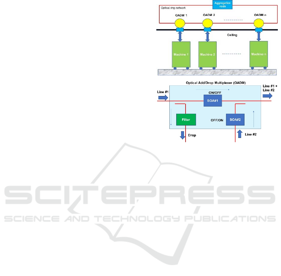
The interconnection network proposed for a group of
10 machines as illustrated in figure 1, is an optical
ring network based on optical add/drop multiplexers
able to switch data optical packets.
Figure 1a shows an interconnection network
deployed in the ceiling of a factory including
distributed optical add/drop multiplexers and one
central aggregation node. The communication inside
this ring exploits WDM channels. WDM channels
can be pure circuits or wavelengths transporting
optical packets or optical frames. Each OADM is
interconnected to a machine through a point to point
link that can be a wired connection or a wireless
connection.
Figure 1b shows the structure of the Optical
Add/Drop Multiplexer used. At its input we have
optical couplers. One coupler is used to drop the
wavelengths. At the output of the drop coupler, an
optical filter is used to select the optical wavelength
from the WDM group of channels. The output of the
filter is then directly connected to the RX not shown
on the figure. For the transit path we use a
Semiconductor Optical Amplifier (SOA) that can
switch very fast (in the range of few ns), that has a
small Polarisation Dependency Loss (few 0.1 dB) and
a fibre-to-fibre gain not exceeding 12 dB to have
linear characteristics. For the add part, we have a
SOA that can be located on the TX part also, and an
optical coupler for the insersion of new
packets/frames in the transit path.
a)
b)
Figure 1: a) Optical ring network considered, b) Optical
Add/Drop Multiplexer (OADM) adopted.
3.2 Performance of the Optical Ring
Network
The optical technology proposed has been evaluated
theoretically and experimentally and the results show
a cascade up to 10 nodes with significant margins,
and BER better than 10
-18
(Chiaroni, 2017). Figure 2
shows the simulated performance obtained for
10 Gbit/s channels through an optical dynamic range
for the input optical power launched in the SOA of
the ODAM transit path. For these simulations we take
into account all the major physical effects : the optical
noise accumulation, the four wave mixing that can be
created in a WDM regime, the PDL and the losses of
each optical component and statistical evolution of
the power per packet/frame per network segment
(from 1dB to 3 dB). We notice that each SOA has a
dynamic loop able to adjust the its gain to correct the
power of the packet/frame. We observe that the
dynamic range is close to 10 dB for dynamic power
variations of 1 dB between consecutive packets and
is close to 4 dB for power variations per network
segment of 3 dB. These results show the high
performance of the optical network proposed for the
evaluation of the Native Ethernet Switching.
Native Ethernet Optical Switching for Deterministic Critical Networks
43
Figure 2: Performance of the ring network.
3.3 Optical Test Bed Used for the PoC
The experimental testbed used for the Proof of
Concept is illustrated in figure 3.
Figure 3a shows a rack including two ring nodes.
We can see on this photo three elements:
the voltage converter box (on the top of the
rack), to transform the alternative 220V into 48
V in continue.
a sub-rack integrating one Optical Add/Drop
Multiplexer. From the right to the left we see:
- a board converting the 48V into +15,-15,+5,
-5 V for the back panel
- a board including optical coupler for
extracting the control channel
- a board including the optical couplers for a
drop part, including an optical filter to select
the wavelength.
- a board including the optical coupler of the
add port.
- a board including optical attenuators to
adject the power injected in the SOAS
- a board including the SOA, its driver and its
dynamic loop for fat power equalization.
- a board including a second optical attenuator
to adjust the power of the insertion channel.
- a board converting the 48V into +15,-15,+5,
-5 V for the back panel
A second sub-rack integrating a second OADM.
We simply notice that the two optical
attenuators have been put on one board to make
the sub-rack more compact.
Figure 3b shows the FPGA board (Xilinx, 2019)
used to generate deterministic Ethernet frames.
Figure 3c shows the configuration tested to enable
a deterministic connection between 3 machines
through an optical ring including two OADMs of the
figure 3a.
a)
b)
c)
Figure 3: a) Photo of two OADMs b) and of the FPGA
board; c) experimental configuration for the PoC.
The TX#1 generates an Ethernet flow, simulating
a machine #1. The data are then crossing the
OADM#1 and are multiplexed with an Ethernet flow
generated by TX#2 simulating a second machine #2.
The reception of the multiplexed data is
performed in the RX#1 whereas RX#2 was used for
monitoring purposes simulating a third machine #3.
PHOTOPTICS 2022 - 10th International Conference on Photonics, Optics and Laser Technology
44
3.4 Electronic Testbed Used for the PoC
The electronical testbed is composed of the following
modules:
an Ethernet frame generator that sends Ethernet
frames from both TX#1 and TX#2 to the optical
testbed. The size of the frames, the sending dates
and the periods of sending are fully
programmable.
a deterministic scheduler that activates or
deactivates alternatively and periodically SOA#1
and SOA#2 of the optical testbed through 2
electrical wires. The date of activation and
deactivation are fully programable.
a frame analyzer that checks if the Ethernet
frames received from the optical testbed on
RX#1 are not corrupted.
An additional module is a signal analyzer that
monitors internal signals from the three previous
modules.
All the modules, as well as the two 10 Gbps
Ethernet sending transceivers (TX#1 and TX#2) and
the two 10 Gbps Ethernet receiving transceiver
(RX#1 and RX#2) have been developed on a Xilinx
FPGA Zynq UltraScale MPSoC zcu102 (Xilinx,
2019).
The clock of the circuitry is set to 257.8125 MHz,
to generate a clock cycle duration of 3.878 ns.
3.5 Control of the SOAs
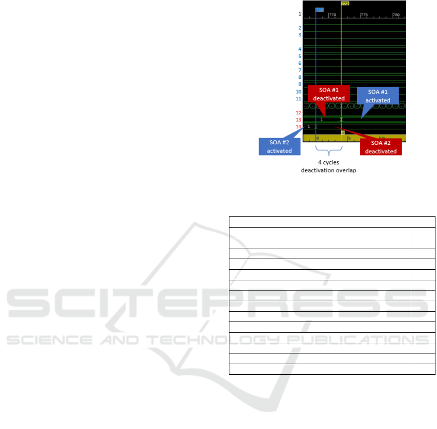
Figure 4 presents the main internal signals monitored
by the signal analyzer previously noted when
switching the input from TX #2 to TX #1.
The explanation of the 14 signals is depicted in
table 1. On the top of the figure the clock cycles are
displayed.
At clock cycle 768 the deactivation signal of SOA
#2 is sent by the deterministic scheduler.
Due to delays needed by SOAs to switch from
10dB (gain of the SOAs) to -40 dB (when the SOA is
in OFF stat), both SOAs are deactivated together
during a given transition time to minimize light power
variations due to an interferometric noise and ease the
clock recovery at the RX level.
Thus, the SOA#1 activation signal is sent 4 clock
cycles later (close to 16.51 ns), i.e. at 772. The
transmission is then disturbed during these 4 clock
cycles transition times.
Figure 4: Main signals monitored.
Table 1: Signals meanings.
Si
g
nal I
d
Cloc
k
1
RX #2 on-going clock recovery signal 2
RX #1 on-going clock recovery signal 3
RX #1 user data 4
RX #2 user data 5
RX #1 well-done frame si
g
nal 6
RX #1 corru
p
ted frame si
g
nal 7
RX #2 user data 8
RX #2 data type 9
RX #2 well-done frame si
g
nal 10
RX #2 corru
p
ted frame si
g
nal 11
Schedulin
g
p
eriod start si
g
nal 12
SOA #1 activation/deactivation control 13
SOA #2 activation/deactivation control 14
Figure 5a) shows the Ethernet frames switched on
a digital scope after optical filtering to reject the
Amplified Spontaneous Emission noise of the SOAs.
On the first trace we see the Ethernet frames
generated by the TX#1 and switched of the SOA #1,
that provides a high On/Off ratio (> 40dB) and
negligible transients during the switching regime. On
the second trace (bottom one) we see the Ethernet
frames generated by TX #2 and switched by the SOA
#2.
Figure 5b) shows the recombination of the
Ethernet frames switches through the optical couplers
in an asynchronous way (no physical
resynchronisation made between the optical paths)
just before the RX #1. We notice also a good power
balance between data generated by the TX # 1 and the
data generated by the TX #2 due to a very low
polarisation sensitivity of the SOAs used (10 dB fibre
to fibre gain, and PDL close to 0.2 dB).
Native Ethernet Optical Switching for Deterministic Critical Networks
45
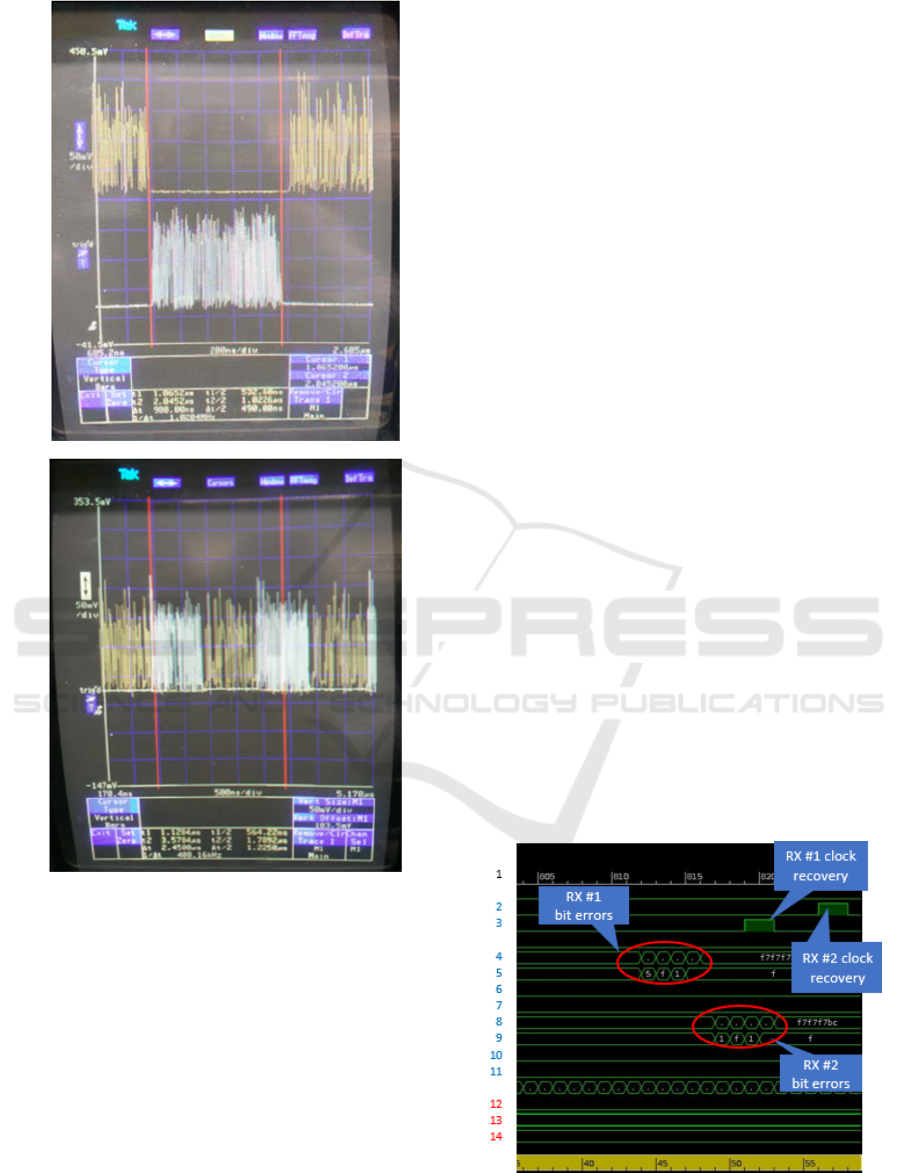
a)
b)
Figure 5: a) Datagram showing data switched at SOA#1 and
SOA#2, b) at the input of the RX#1.
4 EXPERIMENTAL RESULTS
4.1 Objective of the Experimental
Results
In this section we focus on the proof of concept of our
solution. The main objective of this proof of concept
is to demonstrate that it is possible to switch native
Ethernet frames directly in the optical domain without
any buffering. As we have already highlighted, this is
possible for the first time in the optical domain thanks
to our new approach: we use the known Ethernet
frame arrival times to preconfigure the fast-optical
switches. Those arrival times are known for low
latency flows that exhibit regularity like Industry 4.0
ones. As a result, a new optical path is built before
arrival of the Ethernet frame. This new optical path is
then used for transmission of the arriving Ethernet
frame. This is the key difference of our approach with
respect with state of the art. Indeed, current works
focus on minimizing the buffering at the insertion or
at the extraction of data, generally used to encapsulate
or extract Ethernet frames in a new container
including guard bands and a preamble.
4.2 Clock Recovery
The figure 6 shows that at clock cycle 812 RX #1
output becomes erroneous (same problem arises at
RX #2 output at clock cycle 817): during the
switching the Ethernet RX transceivers are in trouble
to decode the signal received from SOA #1 or SOA
#2. The switching generates bit errors for almost 4
clock cycles. The troubles do not arise at same clock
on RX #1 and RX #2 because fiber lengths between
optical testbed and RX #1 and RX #2 are different.
These error bits arise 44 clock cycles after the
switching starts (Figure 4, clock 768) and affect only
dummy bits interleaved between Ethernet frames.
This delay is due to transmissions delay between
scheduler on FPGA card and SOAs, transmissions
delay between SOAs and RX transceivers, serial-
parallel conversion and signal decoding by
transceivers.
RX #1 and RX #2 rise a signal when recovering
clock and data: the switching from SOA#2 to SOA #1
is completed.
Figure 6: Lost of clock during the switching regime of the
SOAs.
PHOTOPTICS 2022 - 10th International Conference on Photonics, Optics and Laser Technology
46
4.3 Transmission Efficiency
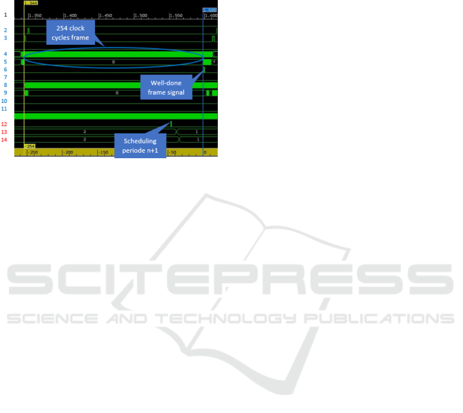
Figure 7 shows the reception of a frame.
Figure 7: Reception of a frame.
For this experiment the periodicity of the
scheduling (i.e. delay between scheduling period n
and scheduling period n+1) is set to 528 clock cycles
(close to 2048 ns). During a period, TX #1 and TX #2
are each multiplexed to RX #1 half of the time.
To check transmission efficiency, the size of the
frames sent by TX #1 is set to the longest possible one
that enable to transmit them without generating errors
due to SOAs de/activation. We experimentally found
a value of 1598 - 1344 = 254 clock cycles.
The frame analyzer checks the received frame and
rises a signal as the received frame is well-done.
As a result, the transmission efficiency is
2 x 254 / 528 = 96 %.
NB: we can note on the figure 7 that, according to
the setup, the frame is also received by RX #2 but is
not checked by the frame analyzer as not expected on
this line which is for measurement only.
5 CONCLUSIONS
We have shown that optical Ethernet frames can be
multiplexed and then switched without the need of
previous opto-electronical conversion or buffering to
introduce a new framing, nor physical
synchronization of the switched optical paths.
The presented novel approach allows for the first
time to switch native Ethernet frames directly in the
optical domain without any buffering. This reduces
transmission delays and prevents the jitter for
applications with strong low latency constraints like
Industry 4.0 ones. Communication flows of these
applications exhibit regularity that we can leverage on
to know in advance the arrival times of the frames.
Further experiments will be performed to evaluate
the impact of dynamic phase shifting and network
scale on the end-to-end frame arrival management.
ACKNOWLEDGEMENTS
The authors acknowledge the colleagues of Nokia
who have participated to these experiments and
William Duluc.
REFERENCES
Dominique Barth, Maël Guiraud, Brice Leclerc, Olivier
Marcé, Yann Strozecki (2018). Deterministic
Scheduling of Periodic Messages for Cloud RAN. ICT
405-410.
Pablo Jesus Argibay-Losada, Dominique Chiaroni and
Chunming Qiao (2020). Optical Packet Switching and
Optical Burst Switching. Springer Handbook of Optical
Networks in November 2020.
Dominique Chiaroni (2017). ANR N-GREEN project: Eco-
designed solutions for a greener ICT in high sensitive
network segments. Plenary speaker, Workshop Green
Days@Sophia, Sophia-Antipolis, June 26-27.
Xilinx (2019). UG1182 - ZCU102 Board User Guide (v1.6).
Native Ethernet Optical Switching for Deterministic Critical Networks
47
