
Residual Stress Analysis of Aluminum-doped Zinc Oxide Films under
Laser-Induced Recovery Process
Yu-Chen Hsieh, Ching-Ching Yang, Chih-Chung Yang, Yu-Hsuan Lin, Kuo-Cheng Huang
and Wen-Tse Hsiao
Instrument Technology Research Center, National Applied Research Laboratories, 20, R&D Rd. VI. Hsinchu Science Park,
Hsinchu City, Taiwan
Keywords: Ultraviolet Laser System, Low-temperature Annealing, Aluminum Doped Zinc Oxide Films,
Induced-crystalline, Residual Stress Analysis.
Abstract: In this study, a low-temperature annealing technique using an ultraviolet laser was proposed for inducing the
crystallization of transparent conductive aluminum-doped zinc oxide (AZO) films. The technique was used
in conjunction with a galvanometer scanner to adjust the laser energy density and scanning speed, thereby
inducing the amorphous crystallization of thin films. X-ray diffraction was used to analyze the structural
properties of annealed thin films. Analysis with different galvanometer scanning speed during annealing and
laser pulse repetition rates during annealing revealed that the two diffraction peaks (i.e., the (002) and (103)
peaks) of the zinc oxide thin films became more noticeable as the laser pulse repetition rate increased. When
the galvanometer scanning speed during annealing was set to 400 mm/s and 600 mm/s, the full width at half
of the maximum (FWHM) of the AZO thin films decreased while the annealing frequency increased. By
contrast, when the annealing speed was 800 mm/s, increasing the annealing frequency caused the FWHM to
decrease and then increase. An analysis of the residual stress of the annealed thin film confirmed that when
the annealing speed was reduced from 800 mm/s to 400 mm/s, increases in laser pulse repetition rate resulted
in increased residual stress.
1 INTRODUCTION
Regarding the development of materials and
techniques used in manufacturing monitors, the three
major materials used for creating thin-film-transistor
(TFT) components are amorphous-silicon (a-Si) thin
films, poly-silicon thin films, and oxide
semiconductors. To meet the requirements of the
wearable-device and Internet of Things industries,
optoelectronic components should be light, thin,
short, and multifunctional. Additionally, in response
to the advocacy for energy-efficient policies, highly
efficient components with low power consumption
have become increasingly prevalent in electronic
products. The resistivity, crystallization (i.e.,
amorphous, crystalline, and polycrystalline), carrier
concentration, and electron mobility of transparent
conductive thin-film materials can affect the
efficiency and power consumption of a thin-film
device. Recrystallization annealing can be used to
address problems concerning the electron mobility
and off-state current of conventional a-Si TFTs.
Conventional methods for changing the crystalline
state of an amorphous thin film include solid-phase
crystallization, metal-induced crystallization, and
excimer laser crystallization. (Coherent, Inc. 2015)
proposed a technique involving the use of excimer
lasers to perform low-temperature a-Si laser
annealing. This technique can increase monitor
resolution and is applicable to large-scale monitors,
active-matrix liquid-crystal displays, active-matrix
organic light-emitting diodes, organic light-emitting
diode televisions, and flexible electronics. (Zhang et
al. 2012) applied nanosecond and picosecond single-
shot lasers to induce the crystallization of Ge
2
Sb
2
Te
5
thin films and plot a curve representing the
relationship between crystallization temperature and
instantaneous laser energy. This enabled examination
of the ablation threshold, melt threshold, solid-phase
crystallization, and melt recrystallization of thin
films. Their experimental results confirmed that
recrystallization could be achieved under the ablation
threshold of Ge
2
Sb
2
Te
5
by using different values of
laser energy density and exposure time to improve the
134
Hsieh, Y., Yang, C., Yang, C., Lin, Y., Huang, K. and Hsiao, W.
Residual Stress Analysis of Aluminum-doped Zinc Oxide Films under Laser-Induced Recovery Process.
DOI: 10.5220/0007363601340138
In Proceedings of the 7th International Conference on Photonics, Optics and Laser Technology (PHOTOPTICS 2019), pages 134-138
ISBN: 978-989-758-364-3
Copyright
c
2019 by SCITEPRESS – Science and Technology Publications, Lda. All rights reserved

characteristics of the material. (Huang et al. 2013)
used relevant theories to conduct an experiment in
which a-Si thin films were exposed to a green-light
nanosecond laser at 532 nm; subsequently, a finite
element analysis was conducted to simulate the melt-
recrystallization process and determine the optimal
energy density. Their experimental results revealed
that the recrystallization temperature and melting
depth varied with the laser exposure time.
Specifically, the results of Raman spectroscopy
revealed that optimal crystallization was achieved
when the energy density was 1000 mJ/cm
2
. By using
excimer lasers to induce the recrystallization of a-
Si/SiO
2
/glass thin films, (Kuo et al. 2007)
investigated the effect of excimer laser during the
melting process on silicon recrystallization, film
thickness, and substrate temperature. They observed
notable changes in film thickness when the melting
duration was increased, particularly at high
temperatures. (Emelyanov et al. 2014) used
femtosecond lasers to induce the recrystallization of
a-Si thin films; specifically, the experiment involved
adjusting the energy density of the laser to identify
the parameters affecting the structure and
photoelectrical characteristics of such thin films.
(Cheng et al. 2014) used a high-repetition-rate
femtosecond laser to induce the crystallization of
transparent conductive thin films composed of
amorphous indium tin oxide (ITO). The results
revealed that with the laser energy of 536 mJ,
repetition rate of 0.05 MHz, and scanning speed of
0.25 mm/s, the crystal structure was perpendicular to
the scanning path (E/C). (Lee et al. 2010) used a 248-
nm krypton fluoride excimer laser to anneal
aluminum-doped zinc oxide (AZO) thin films and
analyze their structure, surface morphology, and
photoelectrical characteristics. The laser energy
density and frequency were fixed at 160 mJ/cm
2
and
10 Hz, respectively, and the laser pulse number
ranged between 600 and 3000. The scanning electron
microscopic analysis revealed that during the laser
annealing process, the pore size of the thin film was
reduced, thereby increasing the grain boundary. The
XRD analysis confirmed that when the number of
laser pulses increased, the diffraction peak intensity
also increased, indicating more favorable crystalline
characteristics. (Tsang et al. 2008) adopted the sol-gel
process to prepare AZO thin films, and a krypton
fluoride excimer laser was used at various energy
levels to anneal the thin films. The XRD analysis
revealed that under a fixed laser pulse number,
increasing the laser energy caused the diffraction
peak values to increase. Similarly, increasing the laser
pulse number under fixed laser energy also increased
the diffraction peak values, indicating that both laser
energy and pulse number affected the thin-film
structure. Investigations of the electrical
characteristics of annealed crystalline structures have
revealed that resistivity noticeably decreases in
response to increases in laser energy. This
phenomenon is attributable to the increased electron
mobility caused by crystal defects and reduced grain
boundary density (Tsang et al. 2008). (Chen et al.
2012) (Chen et al. 2011) used laser beam shaping
techniques to anneal transparent conductive ITO thin
films and fluorine-doped tin oxide thin films. Their
results revealed that laser processing parameters (e.g.,
spot shape, energy distribution, spot overlay, and
operating modes) affected the photoelectrical
characteristics of annealed thin films. In the case of
the fluorine-doped tin oxide thin film, its resistivity
decreased from 7.19 ± 0.55 to 6.70 ± 0.20 × 10
−3
Ω-
cm. (Kim et al. 2011) proposed a low-cost annealing
technique applicable to large-scale metal-oxide thin
films that could be used to manufacture TFT liquid-
crystal displays and flexible electronics. They noted
that conventional annealing chambers require an
annealing temperature of >400 °C, which is
unsuitable for processing the substrates of flexible
electronics; hence, they proposed a low-temperature
manufacturing technique (<200 °C) to anneal four
thin-film materials (In
2
O
3
, a-Zn-Sn-O, a-In-Zn-O,
and ITO). (Morimoto et al. 2012) used a 405-nm
gallium nitride laser diode as the light source for
inducing the crystallization of a-Si TFTs, which were
compared with those with crystallization induced
with commercially available 405-nm, 445-nm, and
532-nm light sources. The results confirmed that a-Si
exhibited a greater absorbance coefficient at 405 nm.
Data from the simulation and experiment regarding
the evenness of the resulting crystalline structure and
efficiency of the crystallization process indicated that
the proposed method can be used to recrystallize and
transform a-Si into micro crystalline Si. (Huang et al.
2016) proposed a 532 nm pulse laser to anneal Al-
doped ZnO films on polyethylene terephthalate (PET)
flexible substrate. By using the laser annealing could
greatly enhance grain crystalline. When the
crystalline size increased and avoid damage to the
PET flexible substrates. (Xu et al. 2018) used light
emission based physical approaches to measure the
driving voltage, reverse current versus relative light
intensity. In addition, the spectroscopic information
shown that the electroluminescence (EL) spectrum
has a broad emitting range of 400-900 nm.
Residual Stress Analysis of Aluminum-doped Zinc Oxide Films under Laser-Induced Recovery Process
135
2 THE PROPOSED
LASER-INDUCED RECOVERY
SYSTEM, SAMPLE PREPARED,
AND RESIDUAL STRESS
ANALYSIS
The proposed low-temperature laser annealing
system contains a Nd:YVO
4
laser source,
galvanometer scanning module, and beam delivery
system. The specifications of the proposed system are
as follows: a laser wavelength of 355 nm, maximal
output power of 14 W, spatial mode of TEM
00
,
maximal pulse repetition rate of 300 kHz, and pulse
width of 30 ns. The galvanometer scanning module
consists of a telecentric lens with a focal length of 163
mm, and its scanning range reaches 60 mm × 60 mm,
which is sufficient for covering the entire annealing
area. The transparent conductive AZO thin film was
prepared first by using a sputtering approach to
deposit the film on a Corning Eagle 2000 glass
substrate (Corning Inc., United States) with an
approximate thickness of 200 nm. To avoid damaging
the glass substrate during the annealing process, the
laser energy was maintained at 61.2 μJ, while the
pulse repetition rate was adjusted to 40, 55, and 70
kHz and the scanning speed was adjusted to 400, 600,
and 800 mm/s. In Bragg’s law (1), d denotes lattice
spacing, θ denotes diffraction angle, and λ denotes X-
ray wavelength (0.154 nm). Accordingly, d decreases
when θ increases, indicating a decrease in film stress.
Therefore, a biaxial stress model can be used to
estimate the residual stress of a thin film during
modification (Jun et al. 2012). Film stress can be
estimated using (2) when it is being analyzed in the c-
axis direction using XRD.
nd sin2
(1)
bulk
bulkfilm
film
C
CC
(2)
where C
bulk
is the lattice strain constant (0.2609
nm) of the ZnO thin film. C
film
was estimated by
substituting the lattice parameter of the AZO thin film
that was derived from XRD analysis into (1). The
surface-layer stress of the thin film can be estimated
using (3) (Jo et al. 2018).
filmf
c
cccc
13
121133
2
13
2
2
(3)
where c
ij
is the elastic constant of ZnO. According
to research on elastic constants (Cebulla et al. 1998),
c
11
= 208.8 GPa, c
12
= 119.7 GPa, c
13
= 104.2 GPa,
and c
33
= 213.8 GPa.
3 STRUCTURE ANALYSIS OF
ANNEALED AZO THIN FILMS
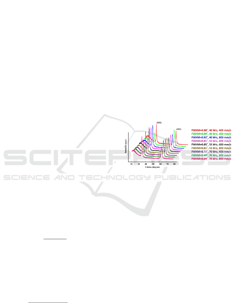
Figure 1 presents the XRD spectra of the AZO thin
films deposited on a Corning Eagle 2000 glass
substrate at different galvanometer scanning speed
during annealing and laser pulse repetition rates (40,
55, and 70 kHz). The spectra exhibited two noticeable
diffraction peaks of the zinc oxide thin films, namely
the (002) and (103) peaks. Increasing the laser pulse
repetition rate caused a substantial increase in the
intensity of the (002) peak. The Scherrer equation is
used for calculating the crystallite size from FWHM
of the (002) peak.
Figure 1: XRD spectrum of AZO films under different
recovery process conditions. (Hsiao et al. 2013).
As indicated in Figure 2, when the galvanometer
scanning speed during annealing was set to 400 and
600 mm/s, the FWHM of the annealed AZO thin film
decreased in accordance with the increasing
annealing frequency. When the galvanometer
scanning speed during annealing was set to 800 mm/s,
the increase in annealing frequency caused the
FWHM to decrease and then increase. These findings
indicated that the grain size of the annealed thin film
was affected by the laser pulse repetition rate and
scanning speed.
The results displayed in Figure 3 revealed that
when the galvanometer scanning speed during
annealing was reduced from 800 to 400 mm/s, the
grain size increased from 7.4 nm to 12 mm. Figure 4
presents the residual stress of the annealed AZO thin
films under the laser pulse repetition rates of 40, 55,
and 70 kHz and scanning speeds of 400, 600, and 800
mm/s; residual stress was calculated using (1)–(3).
The results confirmed that the residual stress of the
thin films increased in accordance with increases in
the laser pulse repetition rate. By contrast, the
PHOTOPTICS 2019 - 7th International Conference on Photonics, Optics and Laser Technology
136
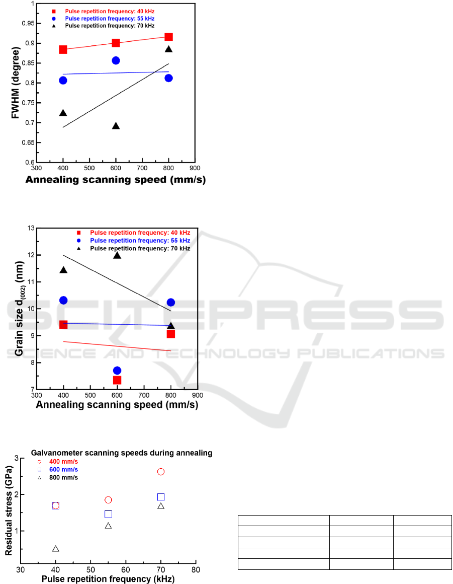
Figure 2: Relationship between FWHM versus different
annealing speeds.
Figure 3: Grain size versus annealing speeds under different
pulse repetition frequency.
Figure 4: Residual stress versus pulse repetition frequency
under different speeds.
residual stress decreased with increasing scanning
speeds under a constant laser pulse repetition rate.
This was attributable to both the increases in pulse
energy of the Nd:YVO
4
laser source in accordance
with the increasing repetition rate and the
accumulation of excessive heat on the thin-film
surface as a result of a low scanning speed.
4 CONCLUSIONS
A low-temperature annealing technique using an
ultraviolet laser was proposed in this study for
inducing the crystallization of transparent conductive
AZO thin films. XRD was used to analyze the
structure of annealed thin films. The resulting XRD
spectra exhibited two noticeable diffraction peaks,
(002) and (103), the intensity of which increased with
an increasing laser pulse repetition rate. The FWHM
of the AZO thin film increased in accordance with
decreasing annealing frequency. When the
galvanometer scanning speed during annealing was
800 mm/s, increasing the annealing frequency caused
the FWHM to decrease and then increase. When the
scanning speed during annealing was reduced from
800 to 400 mm/s, increasing the laser pulse repetition
rate increased the residual stress of the thin film.
Under a fixed laser pulse repetition rate, the residual
stress of the thin film decreased with the increasing
scanning speed during annealing. This was
attributable to two phenomena: the pulse energy of
the Nd:YVO
4
laser source increased as a result of an
increasing repetition rate, and excessive heat
accumulated on the thin-film surface because of the
low scanning speed. Table1 summarizes the stress
under different annealing processes of AZO films (Jo
et al. 2018) (Huang et al. 2016) and (Kim et al. 2017).
In this experiment results indicated that the calculated
the stress values in the annealed AZO films were
approximately less than 3 GPa. During the higher
scanning speed of 800 mm/s, the residual stress were
less than 2 GPa.
Table 1: Specification of the picosecond laser scanning
system.
Authors
Methods
Stress (GPa)
(Jo et al. 2018)
UV +RTA
-0.3 ~ 0.7
(Huang et al. 2016)
Green laser
-
(Kim et al. 2017)
UV + RTA
-
Our present
UV laser
< 3
Residual Stress Analysis of Aluminum-doped Zinc Oxide Films under Laser-Induced Recovery Process
137

ACKNOWLEDGEMENTS
This work was supported in part by the Ministry of
Science and Technology, TAIWAN, numbers MOST
106-2221-E-492 -012 and 107-2622-E-492 -009 -
CC3
REFERENCES
COHERENT, Co. Ltd., 2015. White paper: The digital
display revolution: Built on Excimer laser annealing.
Zhang, K., Li, S., Liang, G., Huang, H., Wang, Y., Lai, T.,
Wu, Y., 2012. Different crystallization processes of as-
deposited amorphous Ge
2
Sb
2
Te
5
films on nano-and
picoseconds single laser pulse irradiation. Physica B,
Vol. 407, pp. 2447-2450.
Huang, L., Jina, J., Shia, W., Yuanb, Z., Yanga, W.,
Caoa, Z., Wanga, L., Zhoub, J., Loub, Q., 2013.
Characterization and simulation analysis of laser-
induced crystallization of amorphous silicon thin films.
Mater. Sci. Semicond. Process. Vol. 16, pp. 1982-1987.
Kuo, C.C., Yeh, W.C., Lee, J.F., Jeng, J.Y., 2007. Effects
of Si film thickness and substrate temperature on melt
duration observed in excimer laser-induced
crystallization of amorphous Si thin films using in-situ
transient reflectivity measurements. Thin Solid Films
Vol. 515, pp. 8094-8100.
Emelyanov, A.V., Khenkin, M.V., Kazanskii, A.G., Forsh,
P.A., Kashkarov, P.K., Gecevicius, M., Beresna, M.,
Kazansky, P.G., 2014. Femtosecond laser induced
crystallization of hydrogenated amorphous silicon for
photovoltaic applications. Thin Solid Films Vol. 556,
pp. 410-413.
Cheng, C.W., Lee, I.M., Chen, J.S., 2014. Femtosecond
laser-induced nanoperiodic structures and simultaneous
crystallization in amorphous indium-tin-oxide thin
films. Appl. Surf. Sci. Vol. 316, pp. 9-14.
Lee, S., Seong, J., Kim, D.Y., 2010. Effects of laser-
annealing using a KrF excimer laser on the surface,
structural, optical, and electrical properties of AlZnO
thin films. J. Korean Phys. Soc. Vol. 56, pp. 782-786.
Tsang, W.M., Wong, F.L., Fung, M.K., Chang, J.C., Lee,
C.S., Lee, S.T., 2008. Transparent conducting
aluminum-doped zinc oxide thin films prepared by sol-
gel process followed by laser irradiation treatment. Thin
Solid Films Vol. 517, pp. 891-895.
Chen, M.F., Lin, K.M., Ho, Y.S., 2012. Laser annealing
process of ITO thin films using beam shaping
technology. Opt. Lasers Eng. Vol. 50 pp. 491-495.
Chen, M.F., Lin, K.M., Ho, Y.S., 2011. Effects of laser-
induced recovery process on conductive property of
SnO
2
:F thin films. Mater. Sci. Eng. B Vol. 176, pp. 127-
131.
Kim, M.G., Kanatzidis, M.G., Facchetti, A., Marks, T.J.,
2011. Low-temperature fabrication of high-
performance metal oxide thin-film electronics via
combustion processing. Nat. Mater. Vol. 10, pp. 382-
388.
Morimoto, K., Suzuki, N., Liu, X., Samonji, K., Yamanaka,
K., Yuri, M., 2012. Amorphous Si crystallization by
405 nm GaN laser diodes for high performance TFT
applications: advantages of using 405 nm wavelength.
Proc. of SPIE Vol. 8244, pp. 824407-1.
Jun, M.C., Park, S.U., Koh, J.H., 2012. Comparative
analysis of Al-doped ZnO and Ga-doped ZnO thin
films. Integr. Ferroelectr., Vol. 140, pp. 166-176.
Cebulla, R., Wendt, R., Ellmer, K., 1998. Al-doped zinc
oxide films deposited by simultaneous rf and dc
excitation of a magnetron plasma: relationships
between plasma parameters and structural and electrical
film properties. J. Appl. Phys. Vol. 83, pp. 1087-1095.
Hsiao, W.T., Tseng, S.F., Huang, K.C., Chiang, D., 2013.
Electrode patterning and annealing processes of
aluminum-doped zinc oxide thin films using a UV laser
system. Opt. Laser Eng. Vol. 51, pp. 15-22.
Huang, L.J., Li, B.J., Ren, N.F., 2016. Enhancing optical
and electrical properties of Al-doped ZnO coated
polyethylene terephthalate substrates by laser annealing
using overlap rate controlling strategy. Ceramic
International Vol. 42, pp. 7246-7252.
Jo, G.H., Kim, S.H., Koh, J.H., 2018. Enhanced electrical
and optical properties based on stress reduced graded
structure of Al-doped ZnO thin films. Ceramic
International Vol. 44, 735-741.
Xu, K., Huang, L., Zhang, Z., Zhao, J., Zhang, Z., Snyman,
L.W., Swart, J.W., 2018. Light emission from a poly-
silicon device with carrier injection engineering.
Materials Science & Engineering B Vol. 231, pp. 28-
31.
Kim, J., Ji, J.H., Min, S.W., Jo, G.H., Jung, M.W., Park,
M.J., Lee, S.K., Koh, J.H., 2017. Enhanced
conductance properties of UV laser / RTA annealed Al-
doped ZnO thin films. Ceramic International Vol. 43,
3900-3904.
PHOTOPTICS 2019 - 7th International Conference on Photonics, Optics and Laser Technology
138
