Conception and Optimization of X Band SIW Band Pass Filter
Otmani Amina, Rahali Bouchra and Benmostefa Naima
STIC Laboratory, Department of Telecommunications, Faculty of Technology, University of Tlemcen, Post Box 230, Pole of
Chetouane, 13000 Tlemcen, Algeria
Keywords: Waveguide, SIW, Bandpass filter, Chebyshev, CST, HFSS, ADS.
Abstract: In this paper, we present methods to design a bandpass filter based on an electronic circuit, a passage was
made to design a filter based on a waveguide fill air and finally, based on a substrate integrated waveguide
SIW. A fourth-order example, in band X, centered on 8.9 GHz with a bandwidth of 400 MHz, is modeled,
simulated and optimized, by three program ADS, HFSS and CST. Very good results were obtained.
1 INTRODUCTION
Newly, a hybrid structure between the waveguides
and the microstriple line has been developed, this
structure called substrate integrated waveguide
(SIW).
The air in the guide is replaced by a dielectric
material (substrate) and the side walls by metal Vias,
while preserving the upper and lower metallization.
The design of passive microwave structures and
in particular filters has an important role in the
manufacture of the various devices (Damou, 2018).
Bandpass filters are one of the essential
components in multiple telecommunication systems,
for that many studies and researches are done to
improve its performance and to miniaturize its sizes.
In this work, we interest in designing and
miniaturize a bandpass filter in the band X.
2 ANALYSIS OF INTEGRATED
WAVEGUIDE
A waveguide is a metal tube filled with air, his
voluminous structure make it difficult to integrate in
the telecommunication means, which become more
and more thin and lightweight (Adabi & Tayarani,
2008).
For solving these problems, the guide is filled by
a substrate of permittivity
, regarding, the side
walls have been replaced by metal vias of diameter
d.
This novel structure is called SIW (substrate
integrated waveguide).
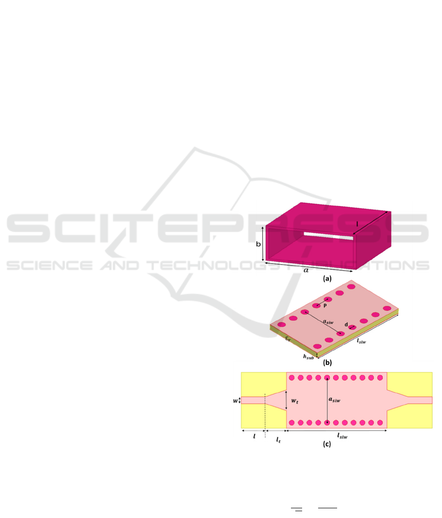
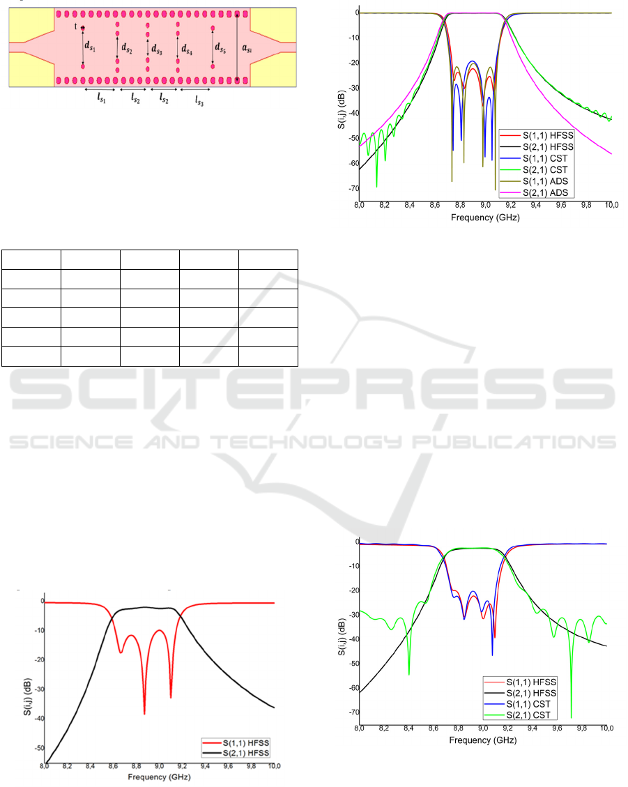
Figure 1: (a) rectangular waveguide (b) SIW (c) SIW with
impedance adapter
The dimensions of SIW can calculated by these
two formulas (Grine, 2018):
√
.
(1)
Amina, O., Bouchra, R. and Naima, B.
Conception and Optimization of X Band SIW Band Pass Filter.
DOI: 10.5220/0009772100670072
In Proceedings of the 1st International Conference of Computer Science and Renewable Energies (ICCSRE 2018), pages 67-72
ISBN: 978-989-758-431-2
Copyright
c
2020 by SCITEPRESS – Science and Technology Publications, Lda. All rights reserved
67
l
√
.
(2)
The transition called taper, was used to realize
the impedance matching between the SIW structure
and that of the microstrip line (feeding line), its
initial dimensions are obtained by the use of the
formulas given in (Caleffo, 2015) and by HFSS
(High Frequency Structure Simulator v13.0) or CST
(Microwave Studio Software v2014.00) we can
optimize them to get a good adaptation.
3 THE DESIGN OF BANDPASS
FILTER
In this paper, a study was done to design a bandpass
filter, with three different components: electronic
circuit, waveguide and SIW structure.
Therefore, steps were followed to calculate the
different parameters of each structure.
3.1 Electronic Circuit Bandpass Filter
The bandpass filter is a filter that lets passes only the
frequencies between two cutoff frequencies (low
cutoff frequency
and a high cutoff frequency
).
Figure 2: Gabarit of Low pass filter, high pass filter and
band-pass filter
2
(3)
Band Width
BW=
(4)
Relative Band Width
FBW=
(5)
A pass-band filter is the combination of low-pass
filter (which lets pass only the frequencies lower
than a desired frequency) and its opposite (high-pass
filter) (Lei et al, 2012).
For that, a transfer function has been applied.
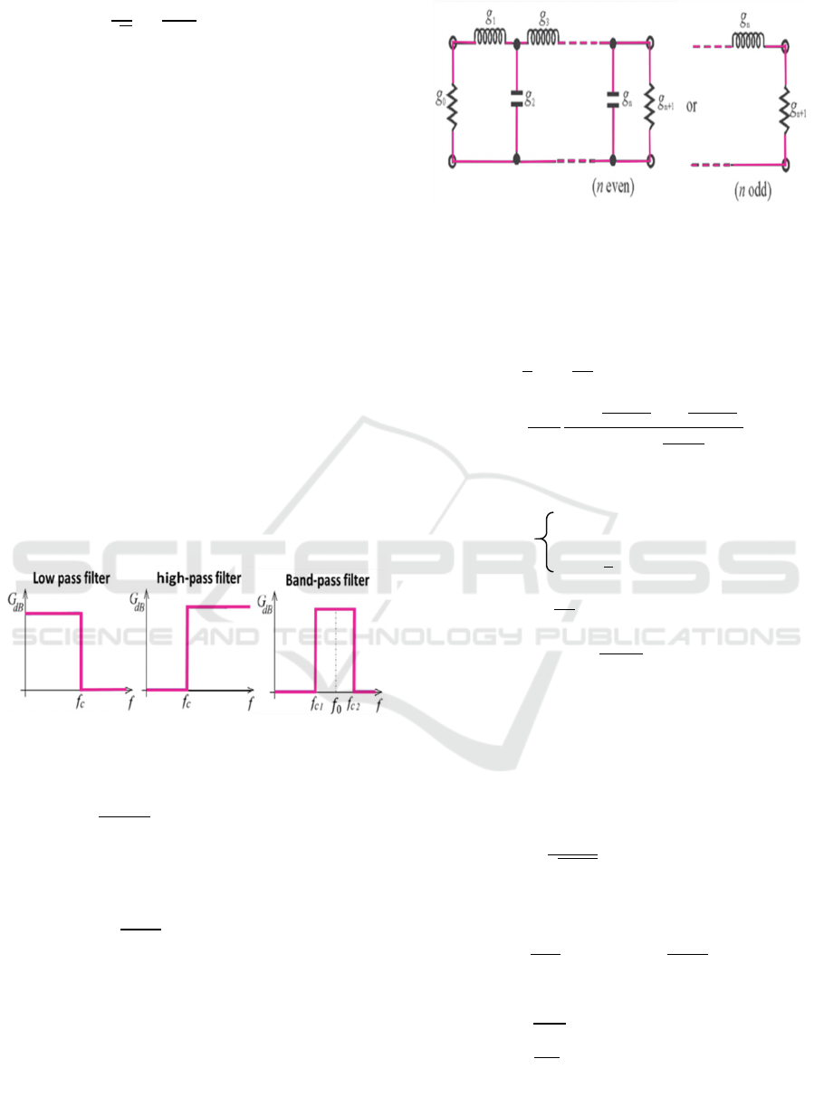
In our case, we used a Chebyshev Low pass
Prototype Filters.
Figure 3: Chebyshev Low pass prototype filters
The equations to calculate the element values for
Chebyshev low pass prototype filters are mentioned
below
1
(6)
2
2
(7)
i=2,3,..n
(8)
=
1 for n odd
for n even
(9)
sinh
2
(10)
ln
17.37
(11)
With
: the passband ripple (dB) (Hong, 2011).
Once, the element values g are calculated, we
can determine the equivalent electronic circuit
values by calculate:
the coupling matrix [M] (Tubail1 & Skaik,
2017)
,
i=1 to n-1
(12)
The external quality factor (Shang et al,
2014)
(13)
Finally,the values of the LC elements
10
(nH)
(14)
10
(pF)
(15)
ICCSRE 2018 - International Conference of Computer Science and Renewable Energies
68
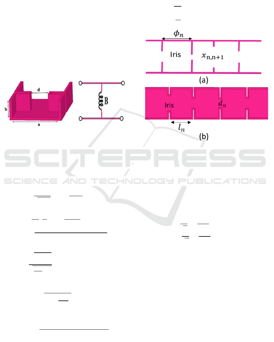
3.2 Bandpass Filter with Inductive Iris
For adding a filter function to a waveguide, we need
to create a discontinuity or a modification inside it.
This discontinuity can be a change in its geometry,
its direction of propagation or one of its physical
parameters (permittivity, permeability).
In our case, two metal plates are inserted in the
waveguide (parallel to the electric field E).
These two plates are symmetrical according to
the size of the waveguide (Vanhoenacker & Vorst,
1996).
The electrical diagram equivalent to this
discontinuity is an inductive susceptance, (Damou,
2018) as shown in the figure 4.
Figure 4: Iris waveguide bandpass filter and his an
inductive susceptance equivalent.
However, to calculate the different parameters of
bandpass filter based on the symmetrical inductive
irises, these steps must be followed:
Calculate the reactance of the iris
,
and
,
,
/1
)
i=0, 1 …n
(16)
,
1
(3
+5
(19)
With
(17)
=
i=0,1,2
(18)
Thecorrespondingguidedwavelengths
And
1
1
m=3,5
(20)
Calculate electrical length between the
irises
( radians)
,
,
i=1, 2,..n
(21)
Finally, the length l
i
between two
consecutive irises, and the width
between two opposite irises ( Zhai et al,
2008).
i=1, 2,..n
(22)
sin
i=1, 2,..n+1
(23)
Figure 5: the parameters of a) transmission line b) iris
waveguide bandpass filter
Once, the initial dimensions of the waveguide are
calculated, it is necessary to optimize them for
respecting the conditions of our specifications.
This operation is made by simulators like HFSS
and CST.
The dimensions of the SIW cavities are
connected to that of the waveguide such that:
√
.
(1)
√
.
(2)
4 DESIGN EXAMPLE
To verify the method given earlier, an example in
the band X [8, 12] GHz was proposed.
Moreover, for facilitating the calculations, we create
under Matlab (Matrix Laboratory v R2014a) a
program that contains the previous equations.
Just enter the data specified for our filter, this
gives us the parameters needed to design it by
electronic circuits and a rectangular waveguide.
For that, and to organize our work well, we have
set this specification:
Conception and Optimization of X Band SIW Band Pass Filter
69
Filter type: Chebyshev, order 4.
The cutoff frequency:
= 6.557 GHz
The center frequency:
= 8.9GHz.
Ripple:
= 0.04321 dB.
Bandwidth: BW = 0.4 GHz.
Relative bandwidth: FBW = 4.494%.
We start with designing the electronic circuit,
therefore, the parameters obtained by the Matlab
program are:
the g values
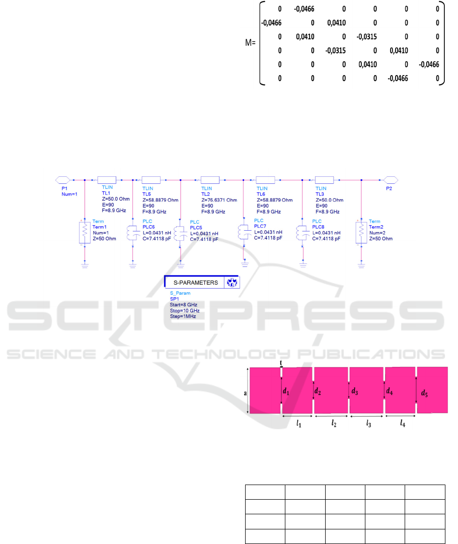
= [1 0.9314 1.292 1.5775 0.7628 1.221]
the coupling matrix
The external quality factor
20.7236
LC elements of resonators
= 0.0431nH
= 7.4118 pF
Figure 6: the bandpass electronical circuit with ADS
After extracting these parameters, they are used
in conceiving the electronic circuit.
This operation is made under ADS (Advanced
Design System v2016.01) software which is
specialized in the design of electronic circuits in
particular, circuits for RF applications .figure(6)
Then, we pass to design the waveguide bandpass
filter.
In this case, the chosen waveguide has a
rectangular section with a=22.86mm and
b=10.16mm.
The equations (16) to (23) was used to determine
the reactances, the electrical lengths, and finally the
different parameters of our bandpass filter (
and
)
figure 7.
These initial dimensions are simulated and
optimized by HFSS and CST. The table 1 illustrates
the final dimensions (the values are in millimeters).
Figure 7: the different parameters for fourth order
bandpass filter
Table 1: the dimensions of bandpass waveguide filter
t
20.1 22.5 22.5 20.1 1
13.1 9.1 8.3 9.1 13.1
Now, we pass to conceive and simulate SIW
structure.
The substrate used in the design is Rogers
RO3006, this substrate is known in microwave
applications for its electrical and mechanical
stability and its competitive price.
ICCSRE 2018 - International Conference of Computer Science and Renewable Energies
70
(
=0.5 mm,
=6.15 and tan(0.0025) are
respectively (the height, the permittivity and loss
tangent) of this substrate
Figure 8: the different parameters for fourth order
bandpass filter
By employing the equations (1, 2) and (24, 25),
It is possible to calculate the different initial
dimensions of the SIW bandpass filter.
Table 2: the dimensions of bandpass SIW filter
D P
10.14 1 1.8 4.27 10
T
7.66 8.7 8.7 7.66 0.49
4.95 3.22 2.89 3.22 4.95
The table 2 illustrates the final values (in
millimeters) of SIW structure (after the optimization
by CST and HFSS)
5 RESULTS AND DISCUSSION
In this work, we design a Chebyshev bandpass filter
of the order 4 in the X band.
Therefore, we set objectives to be achieved.
The initial dimensions obtained are used to
design a waveguide with four symmetrical iris
(figure 7), the results are in figure 9.
Figure 9: Frequency response of the waveguide initial
dimensions (HFSS)
The frequency response shows a filter close to
our desired filter, but it is necessary to optimize it by
the HFSS or the CST.
Figure 10: Comparison of the symmetric iris waveguide
bandpass filter responses (HFSS, CST) and the circuit
results (ADS)
Figure 10 indicates a comparison of symmetric
iris waveguide (HFSS, CST) and circuit (ADS)
responses.
The results show that our specifications are
respected (the center frequency f
0
=8.9 GHz, the
bandwidth BW= 0.4 GHz).
Noted that the S11 for the three responses
(HFSS, CST and ADS) at the passband have three
ripples that means four peaks corresponding to the
order (n = 4) and the reflection levels is less than -20
dB.
Now, we pass to the SIW structure and by using
the optimized dimensions of Table 1, we could
stimulate it on HFSS and validated on CST.
Figure 11: Comparison of the symmetric iris SIW
bandpass filter responses (HFSS, CST)
Conception and Optimization of X Band SIW Band Pass Filter
71
It is very clear that the responses are similar and
confused, and they meet our specifications in terms
of center frequency (f
0
=8.9), of the bandwidth
(BW=0.4 GHz) and even the type of filtering chosen
(Chebyshev) and its order (n=4).
Moreover, the reflection losses in the bandwidth
are below than -20db.
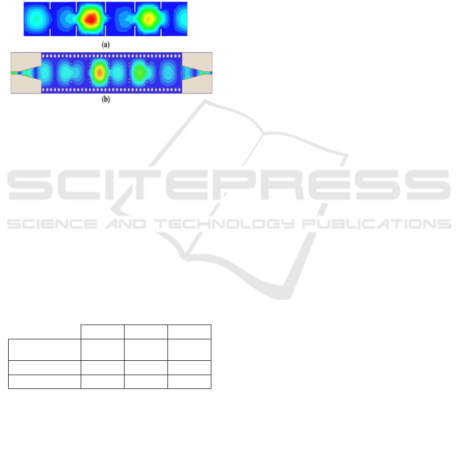
HFSS and CST allow us to map the
electromagnetic field of the structures analyzed, that
is meant, seeing the distribution of the wave TE
10
inside them.
Figure 12: electric fields of the TE
10
mode at f
0
= 8.9GHz
of a) waveguide bandpass filter b) SIW bandpass filter
Figure 12 shows the identical of the
electromagnetic field distribution in the waveguide
and the SIW structure at the center frequency.
For the moment, we designed and simulated two
bandpass filter structures, we analyzed its results, we
found that both of them are respected our
specifications.
So, what makes one of them better than the
other?
To answer this question it is necessary to observe
Table 3, which contains the total dimensions of each
structure.
Table 3: dimensions of each structure
a (mm) L (mm) H (mm)
Waveguide
=1
22.86 131.28 10.16
SIW
=6.15
10.14 63.31 0.664
Reduction % 55.65% 51.77% 93.46%
According to table 3, there is a big difference
between these two structures in terms of dimensions,
such that, the length and width of the SIW structure
are reduced by half, without forgetting the height
which reduced by 93.46%.
Therefore, the dimension factor has a big
importance in the fabrication of the different
devices.
Scientists are currently trying to minimize the
size of components and make them easy to
manufacture and integrate with planar circuits, at a
low cost.
After these studies, we can say that the SIW
structure can meet these requirements.
6 CONCLUSION
In this work, we designed a pass band filter in the
band X by adding inductive iris to two structures the
first is a guide filled with air, the second is a guide
filled with substrate.
As a result, the SIW structure allows us to
miniaturize our filter more than half.
REFERENCES
Adabi, A. & Tayarani, M. (2008). Substrate integration of
Dual inductive post waveguide filter, Progress In
Electromagnetics Research B, 7, 321-329
Caleffo, C. R. (2015). New design procedure to determine
the taper transition for impedance matching between
microstrip line and siw component, Journal of
Microwaves Optoelectronics and Electromagnetic
Applications, 15(3) ,247-260
Damou, M. (2018). Design and optimization of microwave
passive components in SIW technology: Application to
Bandpass filters. PhD thesis Algeria, University of
Tlemcen, Tlemcen.
Hong, J. S, & Lancaster, M. J. CHANG, K (ed.) (2011).
Microstrip Filters for RF/Microwave. 2nd edn, Wiley-
Blackwell, Canada.
Grine, F. (2018). Contribution to the elaboration of a
model of electromagnetic coupling microstrip line -
waveguide integrated into the substrate. PhD thesis
Algeria, University of Constantine 1, Constantine.
Lei, Z. Sheng, S. Rui, L. Chang, K (ed.) (2012).
Microwave bandpass filters for Wideband
communications, Wiley-Blackwell, Canada.
Shang, X. Xia, W. & Lancaster, M. J. (2014). The design
of Waveguide filters based on Cross-coupled
resonators, Microwave and optical technology letters,
56(1), 3–8.
Tubail1, D. & Skaik, T. (2017). A direct approach for
Coupling matrix synthesis for Coupled resonator
diplexers. Journal of Microwaves, Optoelectronics and
Electromagnetic Applications, 16(4), 942-953
Vanhoenacker, D. J & Vorst, A .V. (
1996). Bases de
l'ingénierie micro-onde, De Boeck, Bruxelles
Zhai, Y. Wang, Q. Wang, Z. & Gao, X. X. (2008). The
design of an Iris waveguide filter at 35.75 GHz.
Millimeter Waves GSMM. May 2008, Nanjing, Chine.
IEEE.
ICCSRE 2018 - International Conference of Computer Science and Renewable Energies
72
