
Model of 1D Photonic Crystal Silicon Waveguides by Varying the
Lattice Constant in Their Geometry Stucture via FDTD Method, in
the Field of Communication Photonics for Telco Purpose
Jamilah Husna
1
, Azmi Rizki Lubis
1
, Yusniati
1
, Ahmad Rifqi Md. Zain
2
and Mohd Ambri Mohamed
2
1
Faculty of Engineering, Universitas Islam Sumatera Utara, Medan, Indonesia
2
Institute of Microengineering and Nanoelectronics (IMEN), Level 4, Research Complex, Universiti Kebangsaan Malaysia,
Bangi, Selangor, Malaysia
Keywords: 1D Photonic Crystal, Waveguide, (FDTD), Wavelength Divisionmultiplexing (WDM), Siliconon Insulator
(SOI).
Abstract: The theoretical investigation of tuning a geometry structure of one dimensional (1D) photonic crystal
waveguides based on silicon on insulator (SOI) which has been conducted in UKM lab using Crystalwave
software (FDTD method) is the object of the research. The lattice distance has been varied from 110 nm up
to 165 nm, meanwhile the hole diameter iskept constant at 70 nm. The results show that the main physical
effects of the structure of numerical model could be applied towards the total Q factor and the transmission
performances and the ultrahigh Q factors reached to 3840 and the transmission obtained up to 65%.
1 INTRODUCTION
Photonics have existed as a new research field for
more than ten years. It was founded in the late 1960s,
with the purpose of using light to perform functions
that traditionally fall into the domain of electronics.
Since few years ago, one of the major topics of
interest in photonic research is the study and
development of micro- and nano-structures for fast
signal processing in the telecom window. In addition,
due to their unique ability for manipulating photon
transmission, we assumed that the photonic crystal
(PhCs) will play a significant role in future photonic
and optical applications.
The first successful inventions of photonics such
as laser diode and optical fibers for long-haul data
transmission gave rise to the telecommunication
revolution in the end of the 20 century, which, in
return, became a strong driving force for further
photonic research. With the exception of the past
decade, photonics focused mainly at telecom
applications. Combining or replacing the electronic
circuits by integrated nanophotonic devices should
lead to a dramatic increase in the capacity of
transmitted data (ultra-high band- width with
Wavelength Division Multiplexing) and considerable
reduction of the power consumption. Wavelength
division multiplexing (WDM) is a technology used
for multiplexing signals in optical fibre. The main
advantage of the WDM technique in
telecommunication is that it allows the capacity of the
network to be increased without the need to change
the backbone of the fibr network.
This is made possible through implementing
WDM and deploying optical amplifier throughout the
optical network. The WDM optical spectrum is
divided into several distinct wavelengths that do not
overlap, and each wavelength corresponds to a single
communication channel, thus providing several
WDM channels in the same fiber and greatly utilising
the fibers huge bandwidth. With such large
bandwidth potential, research on WDM devices has
increased with the aim of employing WDM-based
optical backbones for the Internet. The conventional
WDM systems were dual-channel 1.31/1.55 μm
systems including both the minimum dispersion
window and minimum attenuation window.
The WDM consists mainly of two types: Coarse
WDM (CWDM) and Dense WDM (DWDM). In
communication systems, WDM devices show the
ability to improve coherence without losing the
quality of transmission, tightly compact (micrometre
scale) and practical to fabricate on integrated optical
circuits. This is where photonic crystals have much
46
Husna, J., Rizki Lubis, A., Yusniati, ., Rifqi Md. Zain, A. and Ambri Mohamed, M.
Model of 1d Photonic Crystal Silicon Waveguides by Varying the Lattice Constant in Their Geometry Stucture via Fdtd Method, in the Field of Communication Photonics for Telco Purpose.
DOI: 10.5220/0008882200460051
In Proceedings of the 7th International Conference on Multidisciplinary Research (ICMR 2018) - , pages 46-51
ISBN: 978-989-758-437-4
Copyright
c
2020 by SCITEPRESS – Science and Technology Publications, Lda. All rights reserved

potential, as PhC-based WDM for different
wavelength selective-filterin techniques have been
recently realised. Such devices include filter adjacent
to waveguides, using coupling techniques
(Zimmermann et al., 2004) or cavities (Pustai et al.,
2002) for the purpose of achieving PhC-based
wavelength multiplexing and demultiplexing.
Photonic crystals (PCs) are artificial structures
with a periodic dielectric constant in one, two or three
dimensions. They are characterized by photonic band
structures owing to the multiple Bragg scatterings
(Qin et al., 2003). In 1987 the concept of photonic
crystals (PCs) was first proposed by Yablonovitch
and John(Yablonovitch, 1987). They found that by
using periodic arrangement of dielectric mate-rials
which possible for us to control the propagation of the
electro-magnetic waves. If this periodic arrangement
is on the order of the wavelength of light, then for
some range of wavelengtht, it is called Photonic Band
Gap, where in this gap light cannot reach the crystal.
The propagation of light waves is strongly influenced
by the band structures and forbidden in the photonic
band gaps (PBG) (Shiveshwari and Mahto, 2006).
The propagation of a light wave can be manipulated
by PBG. Therefore, many optics effects may be
realized in PCs. By introducing defects into the PBG
structure, for example, resonance modes or defective
modes (Noda et al., 2000).
For the last few years, Photonic crystals (PCs)
structures have attracted, and have been the research
subjects of growing interests. It is well-known, that
the structure is designed to control the propagation of
electromagnetic waves in the same way as the
periodic potential in semiconductor crystals
(Soukoulis, 2006). The dimensional photonic gems
have been referred to for quite a few years as Bragg
reflects. Impedance of the Bragg disseminating is
considered as a reason for the Bragg hole or band
hole. The periodicity makes the band holes rely upon
a few parameters, as the dielectric differentiate
between the utilized materials, and the filling
component of the rudimentary cell. Valuable property
is owned by one gem photonic structure (1D-PC),
which is utilized as an unfortunate optical waveguide,
reflective mirror, optical switch, optical barrier, and
dielectric optical channel.
2 MATERIAL AND METHOD
Silicon on insulator (SOI) was chosen as the main
material to use in this work. A few materials have
been connected with a specific end goal to acquire
one photonic precious stones (1D, for
example,Si/SiO2,SiO2/TiO2,Na3AlF6/ZnSe,Na3Al
F6/Ge(Srivastava and Ojha, 2007). Among the many
existing material frameworks, silicon on cover (SOI)
is considered as the best possibility to create
coordinated nano-photonic gadgets as it permits the
solid reconciliation of optical and electronic gadgets,
that is by staying away from the utilization of half and
half bundling procedures. Silicon PhC structure-
based devices have been used in a wide range of
applications, including light flow control applications
such as waveguides, photonic band gap structures,
and resonators. In this case, all the requirements can
be satisfied by varying one-dimensional photonic
crystal (PhC) structures with narrow\ waveguides in
high refractive index contrast materials, such as
silicon-on insulator (SOI) as reported byLee. (2014).
We then created the defect on one-dimensional
(1D) Photonic crystals waveguide geometry
structure. Furthermore, the brief report regarding the
problem of determining the quality (Q) factor of
localized cavity modes are presented. Each cavity is
formed by introducing a central region with no holes
and tapering the lattice constant and hole size near the
cavity region (McCutcheon and Loncar, 2008). The
observed influence of the presented defect on the
geometry 1DPhotonic crystal cavity structure
waveguide has been conducted. The simulation
results such as the overall characteristics are
investigated.There are the resonance peak
wavelengths, transmission and the Q-performances
affected by the tuning geometry structure in lattice
segment particularly. For further step, we hope the
results from this model devices are considered as
potential building blocks in Silicon-On-Insulator
(SOI) planar photonic integrated circuits operating, in
particular at optical wavelengths for advanced
telecom applications.
As reported that by tuning the
geometry/dimension of the 1-D PhC structures, the
transmission properties can be affected, and by
replacing the homogeneous cavity construction with
double cavities of the normal 1-D PhC, a multi-
wavelengh-transmission optical filter can be realized.
In fact those resonances can be controlled through the
variation of parameters, such as hole dimension,
lattice and cavity lengths (Md Zain et al., 2010).
Some years ago, Srinivasan et al report that if the
cavity has the proper size to support a mode in the
band gap, then light cannot escape, resulting in the
pinning of the mode to the defect (Quan et al., 2010),
and this gave the effect that a resonant cavity is
formed. This structure allows nearly an independent
tuning of each resonant frequency by tuning the
parameters (e.g. width, lattice constant, cavity length)
Model of 1d Photonic Crystal Silicon Waveguides by Varying the Lattice Constant in Their Geometry Stucture via Fdtd Method, in the Field
of Communication Photonics for Telco Purpose
47
each beam and has natural channels for coupling
through each beam to an access waveguide at each
wavelength (Lourtioz et al., 2008), and this pattern
model inspired our model design in our work.
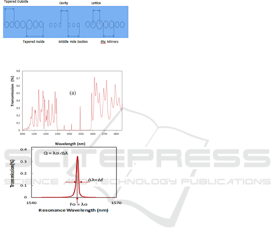
Figure 1: Schematic Design of Hole Pattern of One
Dimensional (1D) Photonic Crystal Cavities Waveguide.
Figure 2: Sketch of 3D FDTD simulation transmission
spectra of the compound photonic crystal cavity waveguide
with multiple resonance results (a), and (b) calculation for
Q factor by Lorentzian fitting.
The three-dimensional (3D) FDTD method has
been used to simulate the designs. We employed the
Crystalwave (Omnisim) software, the available
software in lab, and to overcome some problem
memory leading to large 3D simulations for which we
employed the supercomputer infrastructure at
National University of Malaysia (UKM). Numerical
simulations play an important role for the design and
modelling of guided wave optoelectronic devices. 1D
periodic computational techniques and modelling are
useful and sufficiently well-established
(Joannopoulos et al., 1995). The FDTD method is a
quite general method for the simulation of
electromagnetic devices for all range of frequencies
from the microwave to the optical regime. The power
of the method lies in its simple formulation in which
no restrictive assumptions are made in order to
preserve its applicability to a wide range of problems,
considering a 3D space with no electric or magnetic
current sources, but with materials that present
electric and magnetic conductivity. The last decade
has witnessed dramatic progress and interest in
micro- and nanofabrication techniques of complex
photonic devices (Yee, 1966). FDTD method is
famous due to its large flexibility and extendibility.
Many types of calculations can be performed through
fairly robust algorithms. The design process consists
of engineering three elements: (a) the taper, (b) the
photonic crystal mirror (Phc), and (c) the cavity
length and (d). Middle hole section. The progress in
micro and nanofabrication techniques of complex
photonic devices have been observed. An accurate
quantitative theoretical modelling of these devices
has to be based on advanced computational
techniques that can solve the relevant linear,
nonlinear or coupled partial differential equations
since over last decade (Obayya, 2011).
The proposed waveguide PhC structure that we
presented in this work, consists of a 1D hole array in
a silicon-on-insulator (SOI) photonic wire
waveguide, and the geometry of the proposed
waveguide is as illustrated in Fig. 1. The references
are (Lan and begs) based on the tight requirement of
a WDM system operating to the ITU standard. A
coupled cavity structure was investigated as an ideal
candidate to form a band-pass optical filter based on
1-D PhCs. Based on this, we created the design of
geometry/dimensional structure of one dimensional
(1D) photonic crystal waveguide by placing the three
cavity in that structure, with the purpose to obtain the
multiple peak resonances, good transmissions and
higher Q factor. Numerical simulations play an
important role for the design and modeling of guided
wave optoelectronic devices. 1D periodic
computational techniques and modeling are useful
and sufficiently well-established (Anon, 1995). The
design process consists of engineering three
elements: (a) the taper, (b) the photonic crystal mirror
(Phc), and (c) the cavity length and (d). Middle hole
section. The details of the description of the basic
design can be seen in Fig. 1, where the taper is located
on the external cavity side of the mirror and the row
of seven holes with diameters of 110, 110, 135, 135,
165, 135, 110 nm respectively, and is separated by
increasing distances. Here, between the external
cavities there are several additional tapers as shown
in Fig. 1, the name is the middle hole section taper,
and we keep the those hole diameters at 70 nm. In this
(b)
ICMR 2018 - International Conference on Multidisciplinary Research
48
work, we focus on varying the lattice constant by
varying the lattice distance from 320nm -
355nm.Here, the structure is restructured as follows:
silica (n=1.445) with a thickness of 1100 nm; silicon
(n=3.48) with a thickness of 600 nm; and the last layer
is air (n=1) with a thickness of 1000 nm. For the
adjusting refracting index parameters value for SOI
device structures we keep them constant.
The resonance wavelength, the Q-factor and the
transmission/reflectance performance have been
computed using the Finite Difference Time Domain
(FDTD) approach. The Q-factor results was obtained
from Lorentzian fitting and the description of this
calculation as illustrated in Fig.2.
3 RESULTS AND DISCUSSION
In this study, we try to explore the possibility of
employing more cavities waveguide design
supporting two or more resonances (especially with
both mode design the telecom window). In the other
case, by design, a longer or a shorter of lattice wide,
and/or coupled photonic cavities geometry structure
waveguide and this increases the Q factor and
transmission values. The change in Q depends
strongly on the waveguide properties such as the
width band gap. The other fact shows that the Q factor
value was also affected by other parameters such as
defect and etch. First, we investigated the influence
of the presented defect geometry structure by varying
the lattice constant size and placing three cavities
between the mirror/taper. We define that by applying
325 nm lattice size in geometry waveguide design
which we achieved from the highest Q- factor. The Q-
factor was calculated using λp/Δλ, where Δλ is the
band width of the resonance peak. The spectrum
shows a resonance for the wavelength 1525 nm with
a Q-factor of approximately 3840.
Figure 3: The graph of Q-factor toward lattice constant.
Figure 4: The graph of Multi Resonance wavelength peaks
by varying lattice distance.
We assumed that the higher Q-factors achieved
from simulation in this work probably was caused by
the small of the lattice size. On the other hand, the
simulation results show that changing the geometry
parameters of waveguide has the effect on the
enlargement of the band gap wavelength. This means
that the lattice constant is an important factor in the
performance of the band gap width beside other
parameter. Based on simulation analyzed, we found
that the band gap width becoming larger with the
increase of the lattice size for all the five cases. As
illustrated in fig.3. it shows that the structure exhibits
various band gaps (or stop band) where the photonic
states are not forbidden with the existence of three
resonance peaks for each case/design. The multiple
resonances peak for overall designs were found in
range wavelength area from 1430 up to1690 nm. As
can be seen in Fig. 4. it shows the linear resonance
wavelength peaks resulted of a whole device with
identical geometry parameters, for all case designs. In
addition, Obayya reports that the shift of the
resonance towards longer wavelength can be
explained by a strong nonlinear effect due to the
effect of the magnetic field applied to the structure.
The changing of lattice size modified in this study
has significant effect on the optical response
especially to control the transmittance of the device.
Furthermore, the transmission spectra for a whole
design has been computed and plotted with different
wavelength cantered value for each design. As can be
seen from the graft (Fig.5.) that the transmission
results were varied with a little fluctuation, and
obtained values via transmission spectrum method.
The transmissions obtained were above 30 %, with
the maximum value achieved at 75% when the lattice
size was set at 350 nm. From our perspective, we
310 320 330 340 350 360
1400
1600
1800
2000
2200
2400
2600
2800
3000
3200
3400
3600
3800
4000
4200
Q1
Q2
Q3
Q-Factor
L a ttic e s ize (n m )
310 320 330 340 350 360 37
0
1420
1440
1460
1480
1500
1520
1540
1560
1580
1600
1620
1640
1660
1680
1700
R1
R2
R3
Resonance Wavelength (nm)
Lattice size (nm )
Model of 1d Photonic Crystal Silicon Waveguides by Varying the Lattice Constant in Their Geometry Stucture via Fdtd Method, in the Field
of Communication Photonics for Telco Purpose
49

assume that fluctuation of the transmission values are
due to the numerical errors of the calculations. As
reported in our previous paper that for further
increase, the transmission coefficient peak can be
expected by optimizing the size of the hole radius of
middle hole sections, and with the realization of taper
sections inside the resonant cavity (Husna et al.,
2015). As the Q factor gets higher then the
transmission (T) result will be smaller, and the trend
of the transmission results obtained from our work are
consistent with those previous reports. As overall, the
presented results as illustrated in our calculated
curves (Q- factor, transmission and resonance
wavelength) coincide well and match with the
simulation results in Fig. 2. On the other hand, the
normalized transmission of the resonance varies at
which we believe that the Q-factor and optical
transmission is optimum for a certain cavity condition
as reported by Zain et al., (2015). The other group
researchers supporting our results mention that the
structures may have application to WDM devices in
the range IR to THz, depending on the geometry
(Faneca et al., 2018).
Figure 5: The graft of the normalized transmission spectrum
of 1D photonic crystal cavities waveguide.
4 CONCLUSION
For the conclusion, we successfully investigate the
confine light process in a 1D PhC a silicon waveguide
structure. We have confirmed that it is possible to
modify the geometry of waveguide structure by
varying the number of cavity, lattice, radius and the
number of hole in the periodicity. The wavelength
range in this area (1300 -1550 nm) window has
become very vital in view of the availability of
wavelength division multiplexing (WDM)
transmission system and optical amplifiers (erbium-
doped fiber amplifiers). We found that the model of
1D photonic crystal silicon waveguide designed in
our research is in accordance with properties expected
for different lattice design condition based on
simulation results and it is acceptable to be utilized
for Telco purpose. We optimized that these
wavelengths could be used in a wavelength division
Multiplexing (WDM) system.
REFERENCES
Anon., 1995. Photonic Crystals: Molding The Flow of
Light.
Faneca, J., Perova, T.S., Tolmachev, V., Baldycheva, A.,
2018 One-Dimensional Multi-Channel Photonic
Crystal Resonators Based on Silicon-On-Insulator With
High Quality Factor. Frontiers in Physics. 6(May), 1–9.
Husna, J., Mohamed, M.A., Sampe, J., Zain, A.R.M., 2015
Numerical simulation of one dimensional (1D)
photonic crystal multiple cavities based on silicon on
insulator (SOI). RSM 2015 - 2015 IEEE Regional
Symposium on Micro and Nano Electronics,
Proceedings.
Joannopoulos, J.D., Meade, R.D., Winn, J.N., 1995
Photonic Crystals: Molding the Flow of Light.
Princeton University Press.
Lee, C.C., 2014. The Current Trends of Optics and
Photonics. Springer Netherlands.
Lourtioz, J.-M., Benisty, H., Berger, V., Gerard, J.-M.,
Maystre, D., Tschelnokov, A., Pagnoux, M.D. 2008.
Photonic Crystals.
McCutcheon, M.W., Loncar, M., 2008. Design of a silicon
nitride photonic crystal nanocavity with a Quality factor
of one million for coupling to a diamond nanocrystal.
Optics Express. 16(23), 19136.
Md Zain, A.R., Johnson, N.P., Sorel, M., De La Rue, R.M.,
2010. Design and fabrication of high quality-factor 1-D
photonic crystal/photonic wire extended microcavities.
IEEE Photonics Technology Letters. 22(9), 610–612.
Noda, S., Chutinan, A., Imada, M., 2000. Trapping and
emission of photons by a single defect in a photonic
bandgap structure. Nature. 407(6804), 608–610.
Obayya, S., 2011. Computational Photonics. Wiley.
Pustai, D.M., Sharkawy, A., Shi, S., Prather, D.W., 2002.
Tunable photonic crystal microcavities. Applied
Optics. 41(26), 5574.
Qin, Q., Lu, H., Zhu, S.N., Yuan, C.S., Zhu, Y.Y., Ming,
N.B., 2003. Resonance transmission modes in dual-
periodical dielectric multilayer films. Applied Physics
Letters. 82(26), 4654–4656.
Quan, Q., Deotare, P.B., Loncar, M., 2010. Photonic crystal
nanobeam cavity strongly coupled to the feeding
waveguide. Applied Physics Letters. 96(20), 20–23.
Shiveshwari, L., Mahto, P., 2006 Photonic band gap effect
in one-dimensional plasma dielectric photonic crystals.
Solid State Communications. 138(3), 160–164.
Soukoulis, C.M., 2006. Photonic band gap materials: the
‘semiconductors’ of the future? Physica Scripta. T66,
146–150.
Srivastava, S.K., Ojha, S.P., 2007. Enhancement of
omnidirectional reflection bands in one-dimensional
31032033034035036
0
35
40
45
50
55
60
65
70
75
80
Transmission (%)
Lattice size (nm)
% (R1)
% (R2)
% (R3)
ICMR 2018 - International Conference on Multidisciplinary Research
50

photonic crystals with left-handed materials. Progress
In Electromagnetics Research, PIER 68, 91–111.
Yablonovitch, E., 1987. Inhibited spontaneous emission in
solid-state physics and electronics. Physical Review
Letters. 58(20), 2059–2062.
Yee, K.S., 1966. Numerical Solution of Initial Boundary
Value Problems Involving Maxwell’s Equations in
Isotropic Media. IEEE Transactions on Antennas and
Propagation. 14(3), 302–307.
Zain, A.R.M., Majlis, B.Y., De La Rue, R.M., 2015.
Reproducibility and free spectral range (FSR) control
of a high quality factor-1D photonic crystal (PhC)
extended cavity. RSM 2015 - 2015 IEEE Regional
Symposium on Micro and Nano Electronics,
Proceedings, 1–3.
Zimmermann, J., Kamp, M., Forchel, A., März, R., 2004.
Photonic crystal waveguide directional couplers as
wavelength selective optical filters. Optics
Communications. 230(4–6), 387–392.
Model of 1d Photonic Crystal Silicon Waveguides by Varying the Lattice Constant in Their Geometry Stucture via Fdtd Method, in the Field
of Communication Photonics for Telco Purpose
51
