
Study on Pulsed Voltage Regulation Technology of Precision Plating
Power Su
pp
l
y
Feng Wang, Yongbin Zhang, Guangmin Liu, Qing Wang and Rangjie Wu
Institute of Mechanical Manufacturing Technology, China Academy of Engineering physical, Mianyang, Sichuan, China
fred110@sohu.com
Keywords: Precision electroplating power supply, Pulse voltage regulation, Current acquisition, Verilog HDL.
Abstract: For the existing precision plating pulse power, in order to achieve the precise control of the voltage, the output
voltage can be adjusted from 0 to 7V by changing the duty cycle of the MOSFET. In the system, Altera's
CycloneIV E-series chips are used as the master chip to design the PWM signal generation module, AD9215
current acquisition module and serial communication module. Verilog hardware language is used to write the
program and Modelsim software is used for PWM simulation. The resulting pulse waveform and AD9215
data collected by the observed signaltap, voltage and current data at different duty cycle are recorded by a
high-precision multimeter. Through the analysis of experimental results, the feasibility and correctness of
pulse voltage regulation are verified.
1 INTRODUCTION
The performance of electroplating power is directly
related to the quality of the electroplated coating,
which is one of the important electrical parameters
that affect the performance of the power supply.
When the current density is low, resulting in a small
cathode polarization, coating coarse crystal, or even
no coating. When the current density is too high, it
will make the crystal along the direction of the power
line to the rapid growth of the electrolyte inside, re-
sulting in coating nodulation and dendrites crystalli-
zation, or even burning. When the current density is
very large, resulting in a strong hydrogen evolution of
the cathode surface, PH larger, metal salt mixed in the
coating, so that the coating black. Therefore, the pre-
cise control of the output current parameters is very
important, which can be obtained by the conversion
relationship between the precision resistor and the
voltage. And the voltage parameters are relatively
easier to control accurately. Therefore, it is necessary
to determine the detailed duty cycle and output volt-
age curve, as well as the pulse equivalent and input
voltage curve of the AD sampling components. The
former is conducive to the determination of the initial
value of duty cycle in the voltage feedback link, so as
to shorten the time of voltage regulation, and the latter
is used to determine the intrinsic nature of the device
itself as a reference standard in the voltage regulation
process. In this paper, the pulse voltage regulation
part of the power supply is studied.
2 PULSE VOLTAGE REGULA-
TION TECHNOLOGY
2.1 System Composition
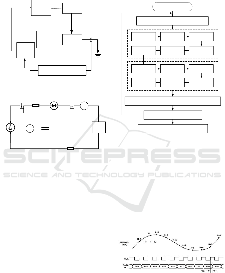
The block diagram of the whole system is shown in
Figure 1. The core of the precision plating pulse
power supply adopts FPGA chip, and the software
module includes the voltage regulation unit, pulse
control unit and current sampling unit, and completes
the functions of PWM pulse voltage regulation, pulse
control and current collection, which AD9215
through the parallel port to the collected data sent to
the FPGA. The system uses closed-loop control, the
feedback current AD sampling results compared with
the set value, according to the size of the difference
between the PWM duty cycle module to produce real-
time adjustment, the driver chip amplification control
Q1 MOSFET, Q2 MOSFET on and off, in order to
achieve Accurate control of the output voltage and
pulse waveform, the circuit diagram shown in Figure
2.
Wang, F., Zhang, Y., Liu, G., Wang, Q. and Wu, R.
Study on Pulsed Voltage Regulation Technology of Precision Plating Power Supply.
In 3rd International Conference on Electromechanical Control Technology and Transportation (ICECTT 2018), pages 503-509
ISBN: 978-989-758-312-4
Copyright © 2018 by SCITEPRESS – Science and Technology Publications, Lda. All rights reserved
503
FPGA
Software
Module
Pulse
Control
Unit
Q1
MOSFET
Q2
MOSFET
parallel
port
AD9215 sampling circuit
10bit
GND
Current
Sampling
Unit
Voltage
Regulation
Unit
Figure 1: System and software peripheral interface logic
diagram.
load
E
V
Q1
Q2
C
R1
R
A
D
Figure. 2: Schematic diagram of power supply circuit.
2.2 Duty Cycle Pulse Voltage Regula-
tion
The duty cycle in this article is equal to the period
divided by the pulse width in order to be programmed
and applied in practice. Using the Pulse voltage regu-
lation mode, the PWM signal generated by the FPGA
logic circuit is used to control the MOSFET, and then
the output voltage is changed, and the PWM signals
controlled by the Q1 MOSFET are obtained by the
FPGA clock 50M crystal frequency. The experi-
mental flowchart of pulse voltage regulation is shown
in Figure 3. The sampling of duty cycle and the sam-
pling points within each step are based on the princi-
ple that the output voltage is linearly changed during
experiment.
Pulse voltage
regulation
Q1 Duty Cycle x (Period / Pulse Width)
Change every 30s
0<x<=20
x=x+1
20<x<=200
x=x+5
200<x<=1000
x=x+20
3000<x<=5000
x=x+200
1000<x<=3000
x=x+100
1000<x<=3000
x=x-100
3000<x<=5000
x=x-200
5000<x<=10000
x=x-500
Record the serial assistant's duty cycle,
current equivalent, voltmeter value, ammeter value
Draw the duty cycle regulator curve,
analyze the data
Change the pulse width of Q1 and
the duty cycle of Q2
200<x<=1000
x=x-20
20<x<=200
x=x-5
0<x<=20
x=x-1
5000<x<=10000
x=x+500
Figure 3: The experiment flow Chart of pulse voltage
regulation of duty cycle.
2.3 Current Acquisition
The AD9215 is used in a current sampling circuit with
a 10-bit data bit and a high performance sample-and-
hold amplifier and output error correction logic with
a signal to noise ratio of 58dBc. The flexible analog
input range is 1V to 2V, using the single power supply
of 2.7V~3.3V. The data format is an offset binary,
with a clock duty cycle stabilizer. The time sequence
diagram of the AD9215 work is shown in Figure 4. In
this experiment, the sampling clock CLK is obtained
by the 50M crystal oscillator of the FPGA.
Figure 4: AD9215 Work sequence diagram.
ICECTT 2018 - 3rd International Conference on Electromechanical Control Technology and Transportation
504
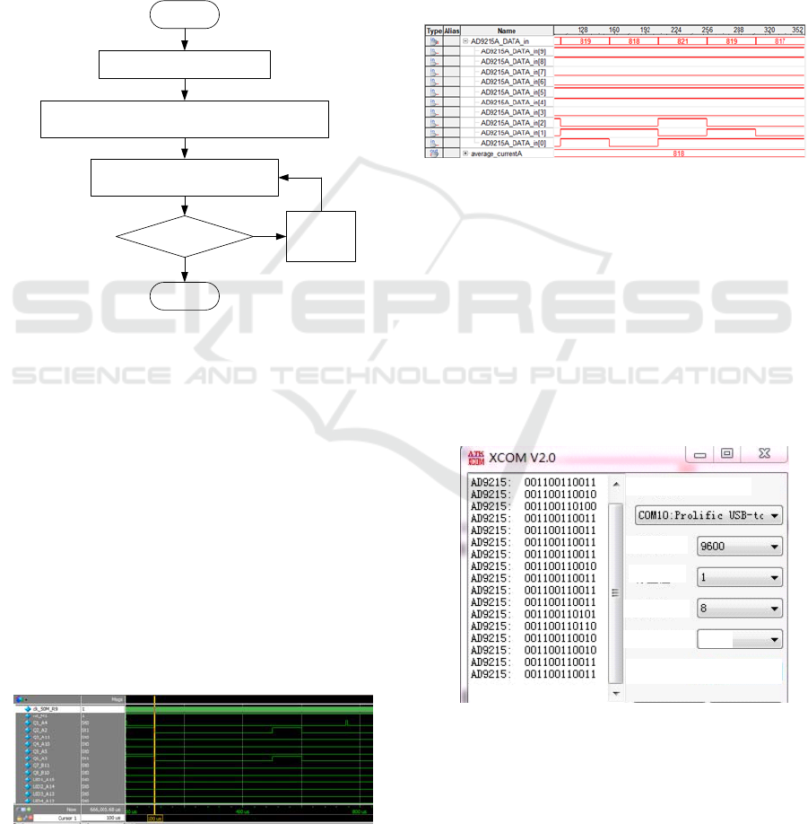
Figure 5 is a flow chart using AD9215 to adjust
voltage, the idea is to set the output voltage value,
according to the duty cycle regulating curve measured
in Figure 3, to determine the Q1 initial value of the
duty, and then to calculate the true voltage value by
AD9215 the current and the output voltage
relationship shown in table 4. Compared with the set
value, the real voltage output value and the set value
are within the error allowable range by adjusting the
Q1 duty cycle continuously.
Start
According to the duty cycle curve to determine
the Q1 initial value of the duty cycle
Set the initial voltage
Determine the actual voltage
based on the current value
To set voltage?
Adjust Q1
duty cycle
End
Figure 5: Flow Chart of AD9215 regulating voltage.
3 SIMULATION AND EXPERI-
MENTAL RESULTS ANALY-
SIS
3.1 Simulation Analysis
Modelsim is a powerful simulation software that of-
fers fast, accurate and easy-to-use features. The prep-
aration of the project file simulation, the results
shown in Figure 6. Q1 MOSFET pulse width of 5μs,
duty cycle of 150. Q2 MOSFET pulse width of 100μs,
duty cycle of 5. Modelsim simulation shows that the
design of the pulse generation method is feasible.
Figure 6: Simulation of pulse generating signal.
Signaltap is an embedded logic analysis tool inte-
grated in Quartus II platform. During the early stage
of FPGA design, signaltap inserts the logic analysis
kernel into the system and can capture multiple sig-
nals inside the chip and store the data in the on-chip
memory. Through the JTAG download line to read
data to the PC, simultaneously display multiple sig-
nals on the monitor to verify whether the desired re-
sults. Observed using signaltap, as shown in Figure 7,
where DATA_in is the value taken at 1MHz, aver-
age_current is calculated by averaging 300 values. It
can be seen that the fluctuations are not large and the
acquisition is very stable.
Figure 7: The acquisition value of the AD9215 observed
by signaltap.
The communication method that the serial port
uses is very simple, the serial port is a one-bit send-
ing. Although sending data much slower than a USB
packet, using two different data lines simultaneously
sends and receives data, the maximum transfer speed
is up to 20Kb/s for low-speed data transfer. Serial As-
sistant to collect data at a baud rate of 9600, the binary
value is displayed, converted to about 818 decimal, as
shown in Figure 8, AD acquisition function is normal
and effective.
Baud rate
Serial port selection
Stop bit
Parity check
Data bit
NO
Figure 8: The acquisition value of the AD9215 observed
by serial assistant.
Study on Pulsed Voltage Regulation Technology of Precision Plating Power Supply
505
3.2 Experimental Results Analysis
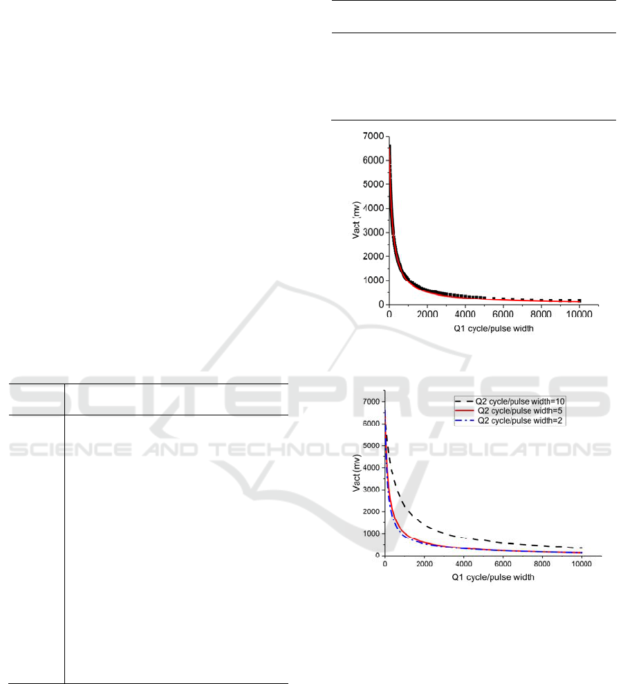
3.2.1 Relation Between Duty Cycle and Out-
put Voltage
Change the Q1 MOSFET duty cycle according to
the design in Figure 3 and record the voltmeter values
while the voltage is stable, as shown in Table 1, tak-
ing one data point from the measured data at approx-
imately 0.5V each. The experimental order and con-
ditions and the fitting function as shown in Table 2,
the argument x is the duty cycle of the Q1 MOSFET,
the variable y is the voltage across the capacitor C,
Q1 MOSFET duty cycle and measured voltage fitting
curve shown in Figure 9 shows. Since the duty cycle
selected in this paper is the reciprocal of the standard
duty cycle, according to the principle of PWM regu-
lator, therefore, first consider the relationship be-
tween voltage and duty cycle inversely proportional
function. The curve is fitted using Eqs. (1), and the
result c is about zero. From Figure 3, the curve and
the data points can be a good match.
y
= 1 / (ax + b) + c (1)
Table 1: The value of Q1 duty cycle and voltmeter under
four kinds of experimental conditions.
Q1 duty
cycle
V1(mv) V2(mv) V3(mv) V4(mv)
1 6340 6480 6600 6600
30 5890 6000 5590 5370
75 5350 5510 4500 4110
135 4800 5000 3600 3154
200 4350 4550 2970 2548
300 3830 4000 2358 2000
400 3429 3600 1965 1666
600 2861 2983 1490 1258
800 2450 2578 1210 1028
1200 1905 2013 885 770
1800 1432 1520 644 580
3000 965 1010 424 400
7000 470 504 199 196
Table 2: The fitting equation under four experimental
conditions
Q1 pulse
width(μs)
Q2 duty
cycle
fitting formula
50 10 y=10^5/(16.155+0.0318x)
1 10 y=10^5/(15.783+0.0295x)
1 5 y=10^5/(15.286+0.0897x)
1 2 y=10^5/(15.225+0.0116x)
(a) Q1 pulse width 50us, Q2 pulse width 50us duty cycle
10.
(b) Q1 pulse width 1us, Q2 pulse width 50us duty cycle
10,5,2.
Figure 9: The relation diagram of Q1 duty cycle and
voltmeter value.
It can be seen from table 2 that different Q1
MOSFET pulse width and different Q2 MOSFET
duty cycle will cause the change of the voltage value
at both ends of capacitance C at the same duty cycle.
When the pulse width and duty cycle of the Q2
MOSFET are unchanged, the pulse width of the Q1
MOSFET changes from 50 μs to 1 μs, and the voltage
value of the latter minus the former voltage value at
the same Q1 MOSFET duty cycle is shown in Figure
ICECTT 2018 - 3rd International Conference on Electromechanical Control Technology and Transportation
506
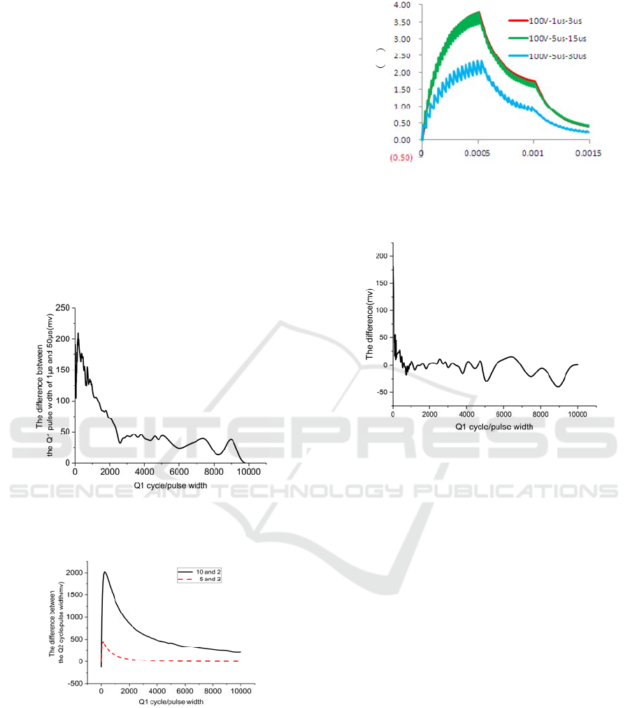
10(a). According to the principle of PWM voltage
regulation, the change of the pulse width of Q1
MOSFET does not affect the voltage value change of
the capacitor C, and the possible reasons are as fol-
lows: on the one hand, the state of the power supply
has changed under the condition of two energizations;
on the other hand, as shown in Figure 11, the simula-
tion shows that when the pulse period, pulse width
and pulse interval of the processing pulse are rela-
tively large, the ratio of the time constant to the dis-
charge is also relatively large, which will cause the
wide range fluctuation of the average gap voltage and
a slight decrease of the voltage amplitude in a certain
range. As the Q1 MOSFET's duty cycle increases, the
voltage difference decreases. The reason is that as the
duty cycle increases, the proportion of the pulse width
decreases, and the effect of fluctuations on the aver-
age voltage decreases.
(a) Voltage difference curve of Q1 pulse width 1μs and
5μs.
(b) Voltage difference curve of Q2 duty cycle 10 and 2, 5
and 2.
Figure 10: The voltage difference under the same
conditions of Q1 duty cycle.
The average voltage
detected
V
Time (s)
Figure 11: The simulation results of average voltage
detection curve.
Figure 12: Voltage difference curve of Q1 duty cycle from
small to large and from large to small.
The constant MOSFET Q1 pulse width changes
the duty cycle of the Q2 MOSFET resulting in the dif-
ference shown in Figure 9 (b). This change corre-
sponds to a change in the load. The duty cycle of the
Q2 MOSFET increases, indicating a decrease in load.
According to the principle of partial voltage, the volt-
age across the capacitor C rises, as shown in Figure
10 (b), which is Q2 MOSFET duty cycle 10 minus the
difference between 2 and 5 minus 2, with Q1
MOSFET duty cycle Increase, the difference in-
creases first and then decreases. As shown in Figure
12, it is the difference diagram of output voltage be-
tween Q1 MOSFET duty cycle from small to large
and from large to small. It can be seen that within the
error allowable range, the measurement way of Q1
MOSFET duty cycle will not have a great effect on
the result.
3.2.2 Equivalent Current Value and Output
Voltage
The Q1 MOSFET duty cycle is changed according to
the design in
Figure 3, and the value of Voltmeter and
Study on Pulsed Voltage Regulation Technology of Precision Plating Power Supply
507

Ammeter are recorded at the same time when the volt-
age is stable. Reference Table 1 corresponds to the Q1
MOSFET duty cycle to take data points, the results
shown in Table 3. The experimental sequence, the
conditions and the fitting function are shown in Table
4, the independent variable x is the equivalent current
value (ammeter value * Q2 MOSFET duty cycle), and
the dependent variable y is the voltage value across
the capacitor C.
Table 3: Q1 duty cycle and equivalent current under the
four conditions.
Q1 duty
cycle
I1(mA) I2(mA) I3(mA) I4(mA)
1 95.5 96.7 100.8 101.8
30 89.6 91.0 84 81.4
75 80.6 83.0 66.1 59.4
135 71.5 74.5 51.05 43.9
200 64.2 67.1 40.75 33.92
300 55.5 58.1 30.7 25.16
400 48.6 51.3 24.25 19.64
600 39.2 41 16.6 13.16
800 32.3 34.2 12.2 9.6
1200 23.6 25 7.2 5.72
1800 16.1 17 3.75 3.08
3000 8.8 9.3 1.15 1.08
As the actual work will not be used below 3mA,
the relevant data will be discarded, the equivalent cur-
rent value and output voltage fitting curve are shown
in Figure 13. It can be seen is a clear linear relation-
ship, the fitting function is Eqs. (2), the specific for-
mula shown in Table 4.
y
= a + b * x (2)
Table 4: Fitting relations under different experimental
conditions.
Q1 pulse
width
(μ
s
)
Q2 duty
c
y
cle
fitting formula
50 10 y=474.5+60.4x
1 10 y=475.9+60.7x
1 5 y=476.1+60.8x
1 2 y=474.5+60.2x
From Figure 13, the curve and data points can be
matched well. The slope represents the resistance
value. In this experiment, R is 51Ω. Therefore, the
equivalent resistance of the other devices in the cir-
cuit is about 10Ω, and the voltage drop of the diode
and other devices is about 475mV. It can be seen that
the Q1 MOSFET pulse width is different and the duty
cycle of Q2 MOSFET is different in the range of error
allowances, which does not affect the value of the
equivalent resistance and the equivalent voltage drop.
Figure 13: The fitting curve of equivalent current and
voltage.
4 CONCLUSIONS
In this paper, according to the existing precision elec-
troplating pulse power supply, the program is pro-
grammed by the PWM voltage regulation principle,
and the effectiveness of the pulse generation is veri-
fied on the Modelsim. The data collected by AD9215
are recorded on signaltap and serial assistants, and the
feasibility of AD acquisition is verified. The duty cy-
cle pulse voltage regulation experiment was designed.
The voltage and current data of different conditions
were measured. The duty cycle voltage regulation
curve and the equivalent current and output voltage
curve were fitted. Analyzed the causes of the change,
calculated the equivalent resistance and equivalent
voltage drop in the circuit, which laid the foundation
for the precise control of the output voltage.
ACKNOWLEDGEMENTS
The authors appreciate the support from the National
Natural Science Foundation of China (Grant No.
51475439) and Sichuan Provincial Science and Tech-
nology Department of application-based projects
(Grant No. 2016JY0109).
ICECTT 2018 - 3rd International Conference on Electromechanical Control Technology and Transportation
508

REFERENCES
Shusen Wang. Study on Pating copper in Cyanide Free
Bath [D]. Dalian Maritime University, 2009: 50-52.
Hua Liu. Research on digital multi-channel pulse ampli-
tude analyzer based on FPGA and preliminary devel-
opment of digital gamma spectrometer [D]. Donghua
University of Technology, 2016: 20-24.
Zhixiang Dong. Research on Modem for Underwater RF
Communication [D]. Dalian University of Technology,
2016: 20-25.
Yongbin Zhang. Detection of Micro-EDM Discharge
Based on Change of Impedance Between Polar Chan-
nels [C] // National Conference of Specialty Processing.
2017: 231-238.
Xiaoming Wang, Yong Zou. Design and working analysis
of a capacitor-regulated surge power source [J] .High
Voltage Engineering, 2007, 33 (6): 25-29.
Xiaokang Liu, Lifeng. Ultra-short pulse micro-electrolysis
process power supply and process test [J]. Journal of
South University of South, 2008, 36 (8): 75-78.
Study on Pulsed Voltage Regulation Technology of Precision Plating Power Supply
509
