
An Optogenetic Platform for Freely Moving Animal Applications
Dimitris Firfilionis, JunWen Luo and Patrick Degenaar
uSystems group, Newcastle University, Newcastle upon Tyne, U.K.
1 OBJECTIVES
In this work, the main objective was to develop a
closed-loop optogenetic platform capable of
performing electrical recording and optical
stimulation in a closed loop manner. The system is
based on an ARM Cortex M4 Microcontroller Unit
(MCU). The MCU is responsible for controlling the
system and, processing and storing the recorded
data. Placing an MCU as a processing unit
significantly increases the flexibility of the system,
as it allows several algorithms and software
architectures to be implemented; this makes the
system suitable for most optogenetic based
applications. As presented by Ramezani et al., a
custom Application Specific Integrated Circuit
(ASIC) is responsible for recording the neural
activity and delivering the optical stimulus. The
recorded and stimulation data are stored on a micro-
SD card. The system is powered by a 155 mAh
Lithium-Polymer (LiPo) battery. Figure 1 illustrates
a conceptual model of the system.
2 METHODS
The system comprises of two main blocks: 1) the
head-stage unit and 2) the embedded control unit.
The head-stage unit contains a neural interface ASIC
responsible for recording neural activity and
delivering optical stimulus. The ASIC is used in
order for the capabilities of the system to be
demonstrated. It requires a 5 V and a 3.3 V supply,
which are provided by the embedded control unit.
The data communication between the two units is
established through a Serial Peripheral Interface
(SPI) link. This makes the system capable of
interfacing with any custom or commercial ASIC,
provided that an SPI link exists on the ASIC to be
used. The head-stage unit contains a microcontroller
unit, a micro-SD card header and a Power
Management Unit (PMU). The system is powered
by a 3.7 V LiPo battery. Figure 2 represents the
proposed system in the form of a block diagram.
2.1 Neural Interface ASIC
A detailed description of the neural interface ASIC
is given by Ramezani et al. It consists of three main
blocks: a) digital controller for external communica-
tion, interpreting and executing commands; b)
neural recording system for amplifying, filtering,
and digitising biopotentials; and c) optical
stimulation system for generating, sequencing and
driving μLEDs providing the systems with
optogenetic neural stimulation capabilities.
For covering the power necessities of the system,
two power domains have been used: 3.3V (using
native devices) and 5V (using thick oxide devices).
The 3.3V supply is used in order for all the
electronics, apart from the optical stimulation output
stage, to be powered. The 5V supply is required to
power the blue μLEDs, due to their threshold
voltage being significantly higher compared to
conventional ones.
Figure 1: Conceptual model of the proposed system.
2.1.1 Digital Control
The digital controller is responsible for providing the
following functions: 1) SPI communication interface
with external processing and control units; 2) a Finite
State Machine (FSM) with defined instructions,
which allow the control of the μLED driving circuits,
Firfilionis, D., Luo, J. and Degenaar, P.
An Optogenetic Platform for Freely Moving Animal Applications.
In Extended Abstracts (NEUROTECHNIX 2018), pages 3-5
Copyright © 2018 by SCITEPRESS – Science and Technology Publications, Lda. All rights reserved
3
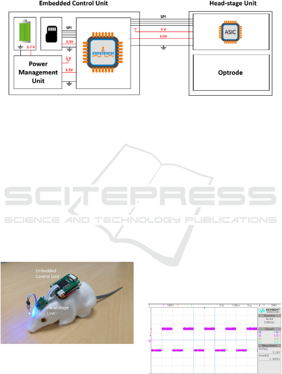
Figure 2: Block diagram representation of the proposed system. On the left the Embedded Control Unit, containing an MCU,
a PMU, a μSD card and a battery. On the right the Head-stage Unit, containing the neural interface ASIC and an optrode. A
5V and 3.3 V supply are provided to the Head-stage Unit, and biderectional data communication is achieved via an SPI link.
as well as the configuration and control of the
acquisition data from the recording circuits.
2.1.2 Neural Recording
The LFP recording sub-system is comprised of four
recording channels, a shared Analog-to-Digital
Converter (ADC) and corresponding control logic.
Each recording channel consists of a low noise Front-
End Amplifier (FEA) to couple to an electrode and
provide low-noise amplification. It also consists of a
2
nd
amplification stage, allowing further
amplification for low noise requirements. As
mentioned previously, the ADC is shared between
multiple recording channels, which raises the
requirement of a buffer with sufficient drive strength,
in order for the settling error and crosstalk between
multiplexing to be reduced.
Figure 3: Physical representation of the proposed system.
The system comprises of the head-stage and control units.
A CREE Light Emitting Diode (LED) has been used for
demonstrating the optical stimulation capabilities of the
system. The LED was turned on through one of the
addressable optical drivers in the ASIC.
2.1.3 Optical Stimulation
The system proposed in [6] allows up to six optical
stimulation sites. Control of the light intensity can be
achieved via a voltage DAC which is then converted
to a current via a transconductance amplifier.
Intensity can be controlled via both pulse width
modulation and intensity control.
2.2 Microcontroller Unit (MCU)
The MCU used in the system is part of the Kinetis
K22F family. It was selected due to its low power
consumption and Digital Signal Processing (DSP)
capabilities. The DSP block enhances the
computational performance of the system allowing it
to accommodate algorithms of various complexities.
It is also responsible for acquiring the digitised data
from the ASIC, performing some computation
according to the selected algorithm and controlling
the optical stimulation system within the ASIC. The
control of the ASIC is achieved through a custom
Finite State Machine (FSM) based software structure
implemented on the microcontroller.
Figure 4: Output voltage of the optical stimulation circuit
(1 second on – 1 second off period).
NEUROTECHNIX 2018 - 6th International Congress on Neurotechnology, Electronics and Informatics
4
2.3 Data Logging
The recorded data, along with information about the
stimulation commands and the algorithm, are stored
in a 1 GB micro SD card. The data is stored to the SD
card though an SPI link. The size of the SD card was
selected to specifically accommodate enough
memory space for a 24 hour continuous recording.
However, depending on the application and power
needs, any alternative memory size could be used.
2.4 Power Management Unit (PMU)
The PMU provides the whole system with 3.3 V and
5 V supply voltages. This is achieved by first
regulating the 3.7 V - provided by a 155 mAh LiPo
battery – down to 3.3 V. The 3.3V are then boosted
up to 5 V, offering enough voltage for the optical
stimulation system. A commercial boost converter IC
was used in order for the 5 V source to be generated.
3 RESULTS
The funcionality of the system was evaluated through
a series of bench top experiments. Both the
stimulation and recording capabilities of the system
were assessed.
3.1 Optical Stimulation
For testing the stimulation circuitry, a CREE LED
was introduced to the output of one of the LED optical
stimulation sites. Two main pulsing sequences were
applied with variations on the intensity level and duty
cycle of the pulse. The first one was a fixed intensity
and fixed duty cycle (1 s ON, 1 s OFF). As shown in
figure 3, the LED could be successully turned on. The
same stimulation pattern was tested for different duty
cycles. Figure 4 represents the voltage at the output
of the optical stimulation circuit.
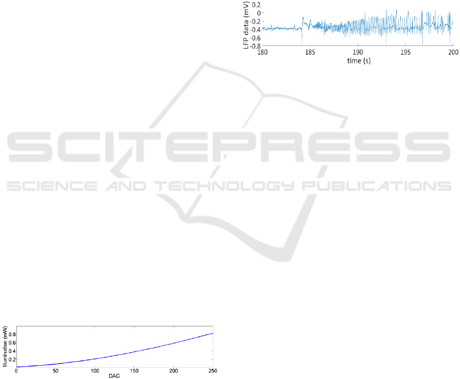
Figure 5: Measured response of LED across output range of
DAC value showing the range of illumination power.
The ability of the optical driver to define different
light intensities by controling the output of voltage
DAC was also tested. For an increasing DAC value,
the current at the output of the stimulation circuit and
the intensity of the LED were increasing accordingly.
Optical measurements we performed by placing the
LED inside and integrating sphere. The measured
results are shown in Figure 5. An optical stimulus of
up to 0.8 mW can be illuminated.
3.2 Electrical Recording
In order for the recording of the system to be tested,
pre-recorded LFP data were introduced inside some
saline solution with the use of a signal generator. The
signal signal was captured from the solution using an
electrode from a Neuronexus probe. Part of the results
(20 seconds) is shown in figure 6.
Figure 6: Pre-recorded seizure data were introduce in the
saline with the use of a signal generator. The signal was
recorded by the Neural ASIC and stored in the SD card. The
figure illustrates part of (20 seconds) the 3-hour continuous
recording. The system was powered off a LiPo battery.
4 DISCUSSION
As presented in the results section, the system
successfully managed to produce stimulation patterns
of various on/off periods and LED light intensities.
The system also managed to record seizure-like data
and store the recorded data on the μSD card. For the
whole duration the system was powered off a 3.7 V
LiPo battery.
REFERENCES
Reza Ramezani, Yan Liu, Fahimeh Dekhoda, Ahmed
Soltan, Dorian Haci, Hubin Zhao, Dimitrios Firfilionis,
Timothy G. Constantinou, Patrick Degenaar, 2018,
“On-probe Neural Interface ASIC for Combined
Electrical Recording and Optogenetic Stimulation”,
IEEE Transactions on Biomedical Circuits and
Systems.
An Optogenetic Platform for Freely Moving Animal Applications
5
