
Atomistic Modelling and Simulation of Transmission Electron
Microscopy Images: Application to Intrinsic Defects of Graphene
Cyril Guedj
1
, Léonard Jaillet
2
, François Rousse
2
and Stéphane Redon
2
1
Univ. Grenoble Alpes, CEA, LETI, 38000 Grenoble, France
2
Univ. Grenoble Alpes, Inria, CNRS, Grenoble INP*, LJK, 38000 Grenoble, France
*
Institute of Engineering Univ. Grenoble Alpes
https://www.minatec.org/fr, http://www.leti-cea.fr/cea-tech/leti, https://www.samson-connect.net
Keywords: Atomistic, Atomic, Modelling, Electron Microscopy, STEM, TEM, Microscopy, Graphene, Defects,
Vacancy, Microstructure, Image, Simulation, Materials, Characterization, Brenner, Samson.
Abstract: The characterization of advanced materials and devices in the nanometer range requires complex tools, and
the data analysis at the atomic level is required to understand the precise links between structure and
properties. This paper demonstrates that the atomic-scale modelling of graphene-based defects may be
performed efficiently for various structural arrangements using the Brenner module of the SAMSON
software platform. The signatures of all kinds of defects are computed in terms of energy and scanning
transmission electron microscopy simulated images. The results are in good agreement with all theoretical
and experimental data available. This original methodology is an excellent compromise between the speed
and the precision required by the semiconductor industry and opens the possibility of realistic in-silico
research conjugated to experimental nanocharacterisation of these promising materials.
1 INTRODUCTION
Digitals tools are more and more required to study,
design and prototype nano-objects, although the
underlying physics is so complex that the quest for a
universal tool is still far from being over. With the
increase of the computational power and the
improvement of the simulation methods, new
possibilities are offered by these tools and even
more shall be expected in the future. The increasing
pace of the semiconductor industry requires rapid
and efficient simulation and modelling strategies to
analyse the results and improve the technological
performances of various nano-devices, sensors or
actuators. In many systems, the optical or electronic
properties are driven by interfacial or by defect-
engineered phenomena. In order to understand the
links between structure and properties, the
nanocharacterisation of materials and devices is
advantageously combined with atomistic modelling
studies. The equilibrium positions of all atoms
provide the necessary basis to simulate the relevant
physical properties, which are measured with
increasing precision and sensitivity. The
combination of experiments conducted in parallel of
simulations is particularly relevant in the field of
transmission electron microscopy (TEM), because
the correlation between the measured image and the
actual arrangement of atoms is not straightforward in
general. Like most characterizations (TEM, X-ray or
electron diffraction, spectroscopic ellipsometry,
scanning tunnelling microscopy, etc.), the precise
simulation of TEM images is usually mandatory to
interpret the experimental results at the atomic scale.
With developments in aberration-corrected
transmission electron microscopy, it is now possible
to characterize vacancy defects in graphene
(Novoselov et al., 2004) at atomic resolution,
enabling the direct comparison between theoretically
predicted structures and experiment. This paper
provides an optimised methodology to perform
atomic-scale modelling of high resolution scanning
transmission electron microscopy (HRSTEM)
experiments of graphene-based defects. For this, it
uses relaxed structural models obtained with the
Brenner module of the Software for Adaptative
Modeling and Simulation Of Nanosystems
(SAMSON) developed by the NANO-D group at
INRIA (www.samson-connect fr). The case of
graphene-based defects is extremely interesting,
Guedj C., Jaillet L., Rousse F. and Redon S.
Atomistic Modelling and Simulation of Transmission Electron Microscopy Images: Application to Intrinsic Defects of Graphene.
DOI: 10.5220/0006829200150024
In Proceedings of 8th International Conference on Simulation and Modeling Methodologies, Technologies and Applications (SIMULTECH 2018), pages 15-24
ISBN: 978-989-758-323-0
Copyright
c
2018 by SCITEPRESS – Science and Technology Publications, Lda. All rights reserved

because this is a 2D material with outstanding
mechanical (Geim and Novoselov, 2007), (Lee et al.,
2008), (Chen et al., 2008), (Pei et al., 2010), (Scarpa
et al., 2009), and electronic (Park et al., 2012); (Lee
et al., 2010) properties. Hence, graphene belongs to
a family of 2D materials which generates huge
expectations in terms of possible applications (Allen
and Kichambare, 2007), (Sorkin and Zhang, 2011)
(Qureshi et al., 2009), (Joh et al., 2013), (Yao et al.,
2009), (Stankovich et al., 2006). The high mobility
of graphene makes it advantageous in the
perspective of post-silicon electronics, but the
defectivity remains a recurrent critical issue. A wide
variety of deviations from a perfect crystal might
occur during the processing of graphene, either due
to the growth conditions or to various sources of
degradation, such as knock-on interactions, electron
or ionic collisions, plasma damage, chemical
reactions, etc. The link between the defectivity and
the electronic, magnetic, optical and mechanical
properties is critical for the device performance.
Thus, the defect engineering is certainly the key of
the possible industrial viability of this material. In
this paper, we study the defects in graphene in terms
of structure and energy. The methodology used to
build the systems and to simulate TEM images is
explained before presenting simulated graphene-
based defects that are compared to available data
from the literature.
2 METHODOLOGY
Many methods exist to simulate hydrocarbon
systems, such as molecular dynamics, Monte Carlo
and the many proposed variants of these approaches.
Typically, these simulations come with ab-initio
quantum-chemistry computations. Therefore,
computational studies of complex defects in
graphene are often limited by a number of atoms
larger than the current first-principle methods can
handle. In all cases, these methods require an initial
structural model consisting in the description of all
atoms in terms of position and chemical nature. In
the case of pure crystals, the 3D periodicity helps in
calculating all the atom positions for large systems
(i.e. more than 50 000 atoms), but in case of
localised asymmetrical defects, this task is much
more tedious or even completely unfeasible in the
worst cases. Hence, a computational tool that is fast
enough to handle physically-relevant calculations
with tens of thousands atoms is highly desirable. The
SAMSON platform and its Brenner module appear
to be ideally suited to this task, since they can handle
complex models and simulate big systems in a
timescale typically less than a day, which is
compatible with the feedback delay required by most
research teams in nanomaterial characterization.
This module appears as an interactive tool for
performing predictive modelling, particularly
adapted to the very sustained pace of
experimentalists and convenient to use, as it is
embedded in a user-friendly software platform.
2.1 SAMSON Software
SAMSON is a software platform for computational
nanoscience developed by the NANO-D group at
Inria and distributed on SAMSON Connect at
https://www.samson-connect.net. SAMSON has an
open architecture, and users customize their
installation with SAMSON Elements, i.e. modules for
SAMSON that may contain apps, editors, builders,
force fields, optimizers, visualizations, etc.
SAMSON Elements are developed with a
provided Software Development Kit, and distributed
on SAMSON Connect as well.
At the time of writing, about fifty SAMSON
Elements are available on SAMSON Connect, for a
number of application domains, including materials
science (e.g. Brenner model, graphene generator,
Universal Force Field, Crystal creator, graphene
TEM image analyser, etc.) and drug design
(GROMACS force fields, AutoDock Vina,
Interactive Ramachandran plots, Normal Modes
Analysis, PEPSI-SAXS, etc.).
Users may mix and match SAMSON Elements
to design their own processes and workflows, and
may use Python scripting to perform modelling and
simulation tasks.
2.2 Brenner Model
To simulate the structure of defects in graphene, the
atomic positions are computed from energy
minimization using the well-known bond-order
Brenner interatomic potential (Brenner, 1990),
(Brenner, 2000), (Brenner et al., 2002), (Dyson and
Smith, 1996), (Los and Fasolino, 2003), (Stuart, et
al., 2000), (Brenner et al., 1996). This is a
parametrized version of Tersoff’s potential which
includes terms to correct for the overbindings of
radicals. Brenner potential is ideally suited to the
interactive digital modelling (virtual nano-
engineering) of complex hydrocarbon structures like
carbon nanotubes (Sinnott et al., 1999), fullerene
(Brenner et al., 1991), or defective single layered
graphene (Lehtinen et al., 2010). We detail below

how the energy and forced can be described from
this potential.
2.2.1 Energy
The Brenner interatomic potential is particular in the
sense that it mostly focuses on covalent bonds (i.e. it
does not consider long-range interaction). Therefore
the potential energy
of the bonding interactions is
a sum over interacting atoms (i.e. separated by less
than 0.2 nm):
=[
−
]
(1)
The details are given in the original reference
(Brenner et al., 2002). Since bonds are defined
dynamically via a bond-order function evolving with
the interatomic distances, this potential has the
ability to describe chemical reactions: it is reactive.
The potential also includes angular and dihedral
terms, radical energetics and the influence of π
bonds (Bosson et al., 2012).
To overcome the lack of long-range interactions,
a non-bonded interaction potential term is added. It
consists in a sum of pairwise potential contributions.
For simplicity, the approach of Los and Fasolino is
chosen (Los and Fasolino, 2002) and the Van der
Waals potential term is added:
=
(
−
)
−
−
(2)
to adjust the precision, using b=3224.9 eV, c
0
=
35.995 nm
-1
, =0.01396 eV and σ=0.344 nm.
2.2.2 Forces
The force terms can be calculated from the gradient
of the potential . More specifically, the Force
applied on atom at position
can be written:
=−
=−
,(,)∈
(3)
where r
ij
is the distance between atoms i and j, and β
is the set of all pairs of atoms involved in the
interaction:
=
(
,
)
,
<
(4)
with
being a threshold distance depending on
the atom types.
2.2.3 Adaptive Brenner
An adaptive version of the Brenner potential has
been implemented in SAMSON (Bosson et al.,
2012). Its interest is that it relies on an algorithm
which incrementally updates the forces and the total
potential energy.
It basically consists in an incremental dynamical
update of the set of interacting atoms and all
information related to one, two, three or four atoms.
Bonds are divided into 4 types: bond with a relative
motion, bonds with a change in potential, bond with
a change in conjugate number, and bonds without
any change in potential. After initialization, all terms
with relative motions are updated incrementally and
after a first level and second level potential update,
the forces are henceforward updated. This allows the
algorithm to linearly scale with the number of
updated bonds. Therefore the computational cost is
decoupled from the number of atoms in the system
and physically-based editing becomes markedly
faster.
To take advantage of adaptive Brenner, an
adaptive mechanism is proposed in SAMSON to
update when minimizing a system. Such an
approach in Cartesian coordinates consists in
deciding for each atom if it might move or be frozen
in space. This decision is made by comparing the
norm of its potential displacement with a threshold
value, either automatically deduced from the system
state or by a manual choice fixed by the user. This
implementation is an extension of the internal
coordinates and articulated bodies simulation
(Redon et al., 2005).
This efficient update mechanism allows
continuous minimization of the system energy
during the edition of the system, which helps to
build realistic structures in a very convenient
manner. The user action step
(creating/moving/deleting atoms) alternates with the
adaptative minimization steps to parallelize the
structure editing and the energy minimization.
2.3 Simulation of Microscopy Images
Once the structure is fully relaxed, it is possible to
compute the corresponding high-resolution scanning
transmission microscopy image by using the
QSTEM software (Koch, 2002). This program
allows accurate image simulations including fully
dynamic calculations. QSTEM computes the true 3D
potential distribution and numerically integrates
every slice of the potential map. This enables a
thickness reduction without limitations in the
multislice calculation. In addition, it is possible to
explore a wide range of experimental setups in order
to evaluate the best conditions to observe the
defects. Here the images are simulated using a

typical voltage of 80 kV, a C3 spherical aberration
of 0.001 mm, a Cc chromatic aberration of 1 mm, an
energy spread of 0.16 eV and a convergence angle
of 20 mrad, which are reasonable values to compare
with high-resolution scanning transmission electron
microscopy (HRSTEM) experiments from an
aberration-corrected microscope. The detectors
collection angle are chosen between 50 mrad and
200 mrad for realistic high-angle annular dark field
(HAADF) conditions. In this conditions of Z-
contrast imaging, the contrast scales with the atomic
number with a power-law dependence (Crewe et al.,
1970). In addition, the HRTEM images are also
calculated with QSTEM using a voltage of 80 kV,
all aberration coefficients equals to zero except for
the chromatic aberration of 1 mm, a spherical
aberration of 5 µm and a vibration of 3 nm in all
directions. In these conditions, the HRTEM
contrasts are usually comparable to HRSTEM, and
the superimposition of the atomic model to the
(S)TEM image provides an efficient method of
validation. To outlines the most striking features, we
have used suitable look-up tables (LUT) to colorize
the experimental TEM and the simulated STEM
images.
3 RESULTS AND DISCUSSION
In the following, we illustrate the cases of typical
defects induced by electron-beam damage during
TEM observation. The probability to observe these
defects is therefore relatively high, for instance
when the electron beam energy is set up above the
threshold for knock-on damage in sp
2
-bonded
carbon structures (i.e. > 100 keV) (Banhart et al.,
1999), (Smith et al., 2001). These defects could also
be obtained by other interactions, such as ionic or
mechanical or by plasma damage, for instance if the
technological processing steps are inappropriate. We
focus the analysis on simple topological defects,
vacancies and adatom, but the same conclusion
applies to all defects we have studied so far
(dislocations, novel phases, extended defects, etc.),
based on available published data.
In the following figures, colorization of
experimental images is obtained with Fiji
(Schindelin et al., 2012) using 16 colors LUT. The
various atomistic models correspond to flake system
of 1308 atoms with flat borders, built in SAMSON
and optimized thanks to the Brenner module. The
clear advantage of the Brenner approach compared
to ab-initio is a ∼ 4 orders of magnitude
improvement in terms of simulation speed.
Moreover, as we will see, the precision achieved is
sufficient to match the experimental results and we
obtained similar findings for all the graphene-based
defects we found in literature, without apparent
limitation, and even for systems with tens of
thousands of atoms. In the following, all
experimental data already published are used with
permissions.
3.1 Stone-Wales Defect
Graphene has the ability to form nonhexagonal
rings, and the simplest example is the Stone-Wales
(SW) defect (Stone et al., 1986) in which four
hexagons are transformed into two pentagons and
two heptagons [SW(55-77) defect] by an in-plane
90° rotation of two carbon atoms with respect to the
midpoint of the C-C bond (Figure 1).
Figure 1: Left: atomistic ball and stick model of the
unstable flat SW(55-77) defect in graphene. Black balls
represent carbon atoms. Right: Corresponding HRSTEM-
HAADF simulated image.
In pure graphene, the C-C bond distance is 0.142
nm according to Pauling (Pauling, 1960), which is
the exact value provided by our code. The
simulation also matches very well previous
experimental results (Meyer et al., 2008), (Kotakoski
et al., 2011) and the corresponding ab-initio
simulations (Li et al., 2005), (Ma et al., 2009).
The planar configuration is unstable and may
relax in the 3D sinelike or cosinelike configuration.
In our case, the minimum energy configuration of 6
eV is obtained for the sinelike configuration (Figure
2), in reasonable agreement with the configuration
and the energy of 5.82 ± 0.03 eV obtained by
quantum Monte Carlo (Ma 2009) and the value of
5.9 eV obtained by DFT-LDA (Jensen et al., 2002).
An absolute comparison with the exact and
precise value of the formation energy is difficult
because of the significant dispersion of formation
energies published in the literature, depending on the
DFT options (LDA, GGA, PW91, PBE, PBE0,
B3LYP, M06-L, vdW-DF, DFT-D, etc.) or the size
of the supercell for instance (Ma et al., 2009), (Li et
al., 2005), (Zhang et al., 2016), (Trevethan et al.,
2014), (Skowron et al., 2015). Meanwhile, the
buckling
height value of 0.156 nm is very close to
the value of 0.161 nm obtained by DFT for the
biggest cell (11 x 11) of Ma et al. (Ma et al., 2009).
The SW defects are not simple planar defects but
rather involve 3D displacements. Our simulation
provides realistic 3D positions of all atoms from a
2D TEM image.
Figure 2: Atomistic model of the lowest energy
configuration SW(55-77) sinelike defect in graphene, with
bond distances, superimposed with the experimental
HRTEM image of Kotakoski (Kotakoski et al., 2011).
Colorization has been added to help the interpretation.
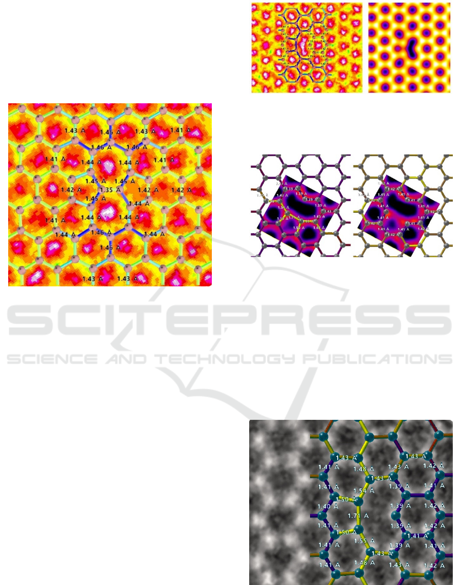
3.2 Monovacancy (V
1
Defects)
3.2.1 Case V
1
(5-9)
The removal of one carbon atom from the graphene
network results in the formation of a single vacancy,
which has been studied both theoretically and
experimentally (Ma et al., 2009), (Li et al., 2005),
(Kotakoski et al., 2011), (Gass et al., 2008), (Meyer
et al., 2008), (Girit, 2009).
Our simulated model matches precisely the
experimental HRTEM images published in the
literature (Figure 3, Figure 4 and Figure 5). We
obtained a formation energy of 5.45 eV, which is
less than the range of [7.6, 7.9] eV obtained by DFT
(Skowron et al., 2015). The symmetric
monovacancy (s-MV) is known to exhibit a Jahn
Teller distortion, and may reconstruct into a closed
five- and nine-membered pair of rings. The
reconstructed monovacancy (r-MV) arrangement
lowers the energy of the symmetrical vacancy
structure in agreement with ab-initio calculations
(El-Barbary et al., 2003).
Figure 3: Left: atomistic model of the V
1
(5-9) defect
superimposed to the colorized experimental HRTEM
image (Kotakoski et al., 2011). Right: simulated
HRSTEM-HAADF image.
Figure 4: Atomistic model of the V
1
(5-9) defect
superimposed to the experimental HRTEM image
published by Robertson (Robertson 2013). Left: r-MV
(also labelled C
2v
). Right: s-MV (also labelled D
3h
).
Another comparison with HRTEM experiment
(Figure 4) shows that the best agreement between
experiment and simulation is obtained for the
reconstructed model r-MV, in expected agreement
with our lowest computed energy. Hence, our
methodology provides a convenient and realistic
approach to model the HRTEM images at the atomic
scale for this case.
Figure 5: Atomistic model of the V
1
(5-9) defect r-MV
superimposed to the experimental HRTEM defect image
entitled “SALVE-III-project-HRTEM-graphene-vacance-
foreign-atoms-defects-zoom.png” obtained by the SALVE
III project (Salve, 2018).

We found similar findings for all the cases we
have studied, without any exception. In general, the
precise comparison with experiment must include
the possible extrinsic contamination by
oxycarboneous species, by hydrogen or by water for
instance to be fully significant, therefore a relevant
comparison should take all these effects into
account.
3.2.2 Case V
1
(5-5)
The V
1
(5-5) state (Figure 6) may be considered as
intermediary between the V
1
(5-9) r-MV and s-MV
(Trevethan et al., 2014). Our calculations predicts a
formation energy of 5.01 eV, which means that such
defect should be observable in principle.
Figure 6: Left: atomistic model of the V
1
(5-5) defect
superimposed to the simulated HRSTEM image. Right:
model superimposed to the experimental HRSTEM image
(Lehtinen et al., 2013).
The simulated HRSTEM-HAADF of Figure 6 is
so close to the image of pure graphene that it might
not be identified in most cases, except perhaps in
ultra-low doses quantitative experiments to
minimize the knock-on energy provided by the
incident electrons and at very low temperatures to
freeze the thermal motion. In the supplementary
movie provided by Lehtinen (Lehtinen et al., 2013),
a pattern similar to the
V
1
(5-5) is possibly obtained,
just prior to the formation of a more extended defect.
Although the contrasts are very rapidly changing,
the
V
1
(5-5) is presumably a reactive seed for more
complex defect growth.
This type of defect has been observed
experimentally with the central 4-fold atom being
substituted by silicon (Ramasse et al., 2013).
3.3 Divacancy (V
2
Defects)
3.3.1 Case V
2
(5-8-5)
When two individual diffusing mono-vacancies meet
they will coalesce into a nearest-neighbour di-
vacancy defect (equivalent to removing a carbon
dimer from the lattice). This process results in the
formation of the stable pentagon–octagon– pentagon
(5–8–5) structure, which has been widely observed
in high-resolution transmission electron microscopy
(HRTEM) images (Kotakoski et al., 2011), (Warner
et al., 2012), (Lehtinen et al., 2013) (Robertson and
Warner 2013). Our calculation provides a formation
energy of 7.29 eV, not far from 7.59 eV by DT-LDA
(Saito et al., 2007) and 7.52 eV by Tight Binding
(Xu et al., 1993), (Dettori et al., 2012).
Figure 7: Left: atomistic model of the V1 (5-8-5) defect
superimposed to the colorized experimental HRTEM
image (Kotakoski et al., 2011). Right: simulated
HRSTEM-HAADF image.
The comparison with experiment (Figure 7) is
once again very positive, with a nearly perfect match
with published experimental TEM results.
The
V
2
(5-8-5) defects may mutate into the V
2
(555-777) and V
2
(5555-6-7777) states due to
electron beam irradiation for instance, and these
transitions were observed by HRTEM (Robertson,
2012), (Kotakoski et al., PRL 2011), (Kotakoski et
al., PRB 2011).
3.3.2 Case V
2
(555-777)
The structure of the V
2
(555-777) divacancy is
displayed in Figure 8, showing an excellent
agreement between experiment and simulation.
Figure 8: Left: atomistic model of the V
1
(555-777) defect
superimposed to the colorized experimental HRTEM
image (Kotakoski et al. 2011). Right: simulated
HRSTEM-HAADF image.
The calculated formation energy is 7.14 eV, in
reasonable agreement with the value of 7.41 eV
obtained by DFT-PBE/DNP (Wu et al., 2013).
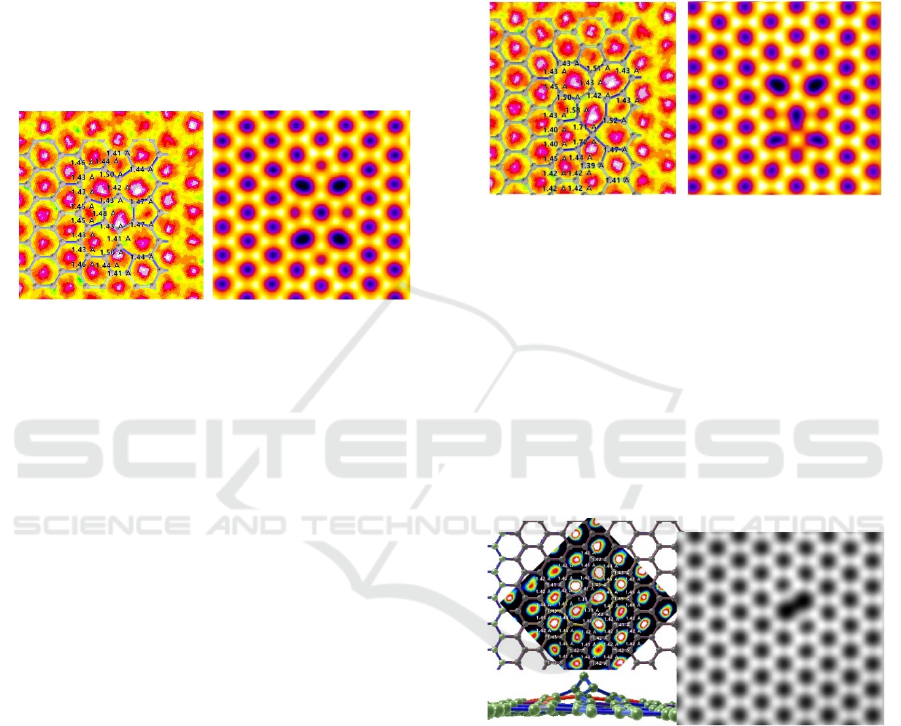
Hence the
V
2
(555-777) state should be more stable
than the
V
2
(5-8-5), in agreement with all DFT
results published (Skowron et al., 2015).
3.3.3 Case V
2
(5555-6-7777)
The divacancy state V
2
(5555-6-7777) is represented
in Figure 9, superimposed to the experimental
HRTEM image attributed to this defect by
Kotakoski. Surprisingly, the matching is not perfect
and the TEM image appears asymmetrical as
opposed to the simulated image.
Figure 9: Left: atomistic model of the V
2
(5555-6-7777)
defect superimposed to the colorized experimental
HRTEM image (Kotakoski et al., 2011). Right: simulated
HRSTEM-HAADF image.
The computed formation energy is 7.45 eV, close
to the DFT value of 7.08 eV (Wu et al., 2013).
According to our simulation, this defect should be
less stable than the
V
2
(5-8-5), whereas Wu predicts
the opposite conclusion.
To understand this apparent contradiction, we
have tried to obtain a better match to the
experimental results, because we believe that
ultimately Nature is never wrong. This corresponds
to the trivacancy case as reported below.
3.4 Trivacancy (V
3
Defects)
3.4.1 Case V
3
(5555-666-77)
A set of studies is devoted to the structure and
energetics of trivacancies in graphene obtained by
structure reconstruction rearrangements after
removing 3 carbon atoms (Dai et al., 2011), (Faccio
et al., 2012), (Saito et al., 2007). Experimentally, the
trivacancy state may be obtained for instance by
bombardment with energetic particles (Wang et al.,
2012). The
V
3
(5555-666-77) structure has not been
studied to our knowledge, yet it apparently provides
the best agreement (Figure 10) with the experimental
image tentatively attributed to the
V
2
(5555-6-7777)
by Kotakoski et al., (2011).
This novel defect structure has a formation
energy of 12.54 eV. We therefore suggest that this
trivacancy may occur during e-beam irradiation.
This case highlights particularly well the interest of
our methodology which offers a new way to explore
in-silico novel types of defects, perhaps
unpublished, and yet observed experimentally by
HRTEM or HRSTEM.
Figure 10: Left: atomistic model of the V3 (5555-666-77)
defect superimposed to the colorized experimental
HRTEM image tentatively attributed to the V2 (55555-6-
7777) defect (Kotakoski et al., 2011). Right: simulated
HRSTEM-HAADF image.
3.5 Carbon Adatom
The healing (self-repair) of various graphene defects
by migration of adatoms has been observed by
HRTEM (Song et al., 2011), (Robertson et al.,
2012). The result of our calculation is displayed in
Figure 11.
Figure 11: Left: atomistic model of the 1C adatom defect
superimposed to the colorized experimental HRTEM
image extracted from the supplementary movie 6 provided
in (Lehtinen et al., 2013). Right: corresponding simulated
HRSTEM-HAADF image.
DFT studies usually gives three stable positions
of the adatom on graphene (Tsetserisa and
Pantelides, 2009). The bridge position is predicted to
be the most stable and was observed by HRTEM
(Hashimoto et al., 2004) and by HRSTEM ( Bangert
et al., 2009). We obtain a formation energy of 2.69
eV, therefore such defect should form easily during
processing of a graphene-based nanodevice. The
DFT method provides a value of the order of 1.5-2

eV for the binding energy of the carbon adatom (Lee
et al., 1997); (Lehtinen et al., 2003). The
perpendicular distance of the adatom to the graphite
surface is ∼ 0.222 nm, not too far from the value of
0.187 nm previously obtained by ab-initio
calculations for 50 atoms (Lehtinen et al., 2003). In
our case, we find that the 5
th
nearest neighbours
around the carbon adatom are vertically displaced,
therefore a simulation box of 50 atoms is certainly
too small to simulate the full relaxation of the
structure. Indeed, we obtained that 192 atoms are
vertically displaced by more than 0.005 nm around
the carbon adatom. Our methodology therefore
provides extended strains and stresses over long
distances, which is not possible with other methods
restricted to a limited number of atoms.
3.6 Extended Edge Defect (88-7-5555)
A severe test to assess the validity of a structural
model consists in considering a complex defective
structure with a large number of atoms. Hence, we
have used an extended defect and the excellent
spatial resolution obtained by the Salve project
(Salve, 2018) to check our methodology. The double
correction of chromatic and spherical aberrations
provides information transfer until 71 pm, which is
probably the best result ever obtained for an image
of graphene. The comparison is depicted in Figure
12. As usual, a nearly perfect agreement between
simulation and experiment is obtained.
Figure 12: Left: atomistic model of the extended defect
88-7-5555 defect superimposed to the experimental
HRTEM image entitled “SALVE-III-project-HRTEM-
graphene-vacancy-characteristic-defects.png” (Salve,
2018). Right: corresponding simulated HRTEM image.
The simulation also provides the distortion maps
for all bonds, in 3D and with picometric spatial
resolution. The positions of all atoms in the system
are therefore extracted and are readily available for
further ab-initio calculations in order to get all the
physical properties (electronic, optical, mechanical,
magnetic, etc.).
4 CONCLUSIONS
Using the Brenner module of the SAMSON
platform, we have precisely matched the
experimental high resolution transmission electron
microscopy experiments of various graphene-based
defects. We have also shown that a good agreement
is obtained with more complex ab-initio simulations
in terms of structure and energy. This methodology
opens the pathway to more extensive in-silico
exploration of all forms of phases or defects in
carbon-based materials, like diamond-like carbon
(DLC), amorphous carbon, nanotubes, fullerenes,
pentaheptite (Crespi et al., 1996), or other novel
phases or defects. Apparently, there is virtually no
limit in the number of structural arrangements of
graphene-based defects that can be simulated with
the Brenner module of SAMSON, in good matching
with experimental results. Finally, this methodology
is therefore a reliable approach to obtain 3D
atomistic models from 2D experimental TEM
images.
In the future, we would like to extend such a
methodology to study in detail the possible
transitions between different types of defects.
ACKNOWLEDGEMENTS
The invaluable contribution from the platform of
nanocharacterization (PFNC) at MINATEC,
Grenoble, France is respectfully acknowledged
(https://www minatec.org/en/). We would like to
gratefully acknowledge funding from the European
Research Council through the ERC Starting Grant
No. 307629.
REFERENCES
Allen, B.L. et al., 2007. Carbon nanotube field-effect-
transistor-based biosensors, Adv Mater, 19 (11), pp.
1439-1451.
Ansari R. et al., 2012. Mechanical properties of defective
single-layered graphene sheets via molecular
dynamics simulation. Superlattices and
microstructures, 51, 274-289.
Bangert U. et al., 2009, Nanotopography of graphene,
Phys. Status Solidi A, 206, 2115–2119.
Banhart F. et al., 1999. Irradiation effects in carbon
nanostructures, Rep. Prog. Phys. 62, 1181.
Banhart F. et al., 2011, Structural defects in graphene,
ACS Nano, 5(1), pp 26-41.

Bosson et al., 2012. Interactive physically-based structural
modeling of hydrocarbon systems, J. of
Computational Physics, vol. 231, 6, p 2581-2598.
Brenner D.W. et al., 1996. Simulated engineering of
nanostructures, Fourth Foresight Conference on
Molecular Nanotechnology.
Brenner D.W., 1990. Empirical potential for hydrocarbons
for use in simulating the chemical vapor deposition of
diamond films, Phys. Rev. B, 42, 9458-9471.
Brenner D.W. et al. 1991, Molecular dynamics
simulations of the nanometer-scale mechanical
properties of compressed
Buckminsterfullerene”, Thin Solid Films 206, 220–223.
Brenner D.W., 2000. The art and science of an analytic
potential, Phys. Stat. Sol. (b) 217, 23–40.
Brenner D.W. and al. 2002, A second-generation reactive
empirical bond order (REBO) potential energy
expression for hydrocarbons, J. Phys.: Condens.
Mater. 14, 783–802.
Chen H. et al., 2008. Mechanically strong, electrically
conductive, and biocompatible graphene paper, Adv.
Mater. 20 (18), pp 3557-3561.
Crespi V. H. et al., Prediction of a pure-carbon planar
covalent metal, Phys. Rev. B 53, R13303(R) (1996)
A. V. Crewe, J. Wall, and J. Langmore, Science 168, 1338
(1970).
Dai X. Q. et al., 2011. First-principle study of magnetism
induced by vacancies in graphene, Eur. Phys. J. B, 80,
343–349.
Dettori R. et al. 2012, Elastic fields and moduli in defected
graphene, J. Phys.: Condens. Matter, 24, 104020.
Dyson A.J. and Smith P.V., 1996. Extension of the
Brenner empirical interatomic potential to C–Si-H
systems. Surf. Sci. 355, 140–150.
El-Barbary A.A. et al., 2003. Structure and energetics of
the vacancy in graphite, Phys. Rev. B 68, 144107.
Faccio R. et al., 2012. Magnetism in multivacancy
graphene systems, J. Phys.: Condens. Matter, 24,
375304.
Gass M.H. et al., 2008. Free-Standing Graphene at Atomic
Resolution, Nat. Nanotechnol, 3, 676–681.
Geim A.K. and Novoselov K.S., 2007. The rise of
graphene, Nat. Mater 6, pp 183-191.
Girit Ç Ö. Et al., Graphene at the Edge: Stability and
Dynamics, Science 27 Mar 2009, Vol. 323, Issue
5922, pp. 1705-1708
Hashimoto A. and al., 2004. Direct evidence for atomic
defects in graphene layers, Nature, 430, 870–873,
DOI: 10.1038/nature02817
Jensen P. and al. 2002. Catalysis of nanotube plasticity
under tensile strain, Phys. Rev. B, 66, 193403.
Joh H.-I. et al., 2013. Synthesis and properties of an
atomically thin carbon nanosheet similar to graphene
and its promising use as an organic thin film transistor,
Carbon, 55, pp. 299-304.
Koch C., 2002. Determination of core structure periodicity
and point defect density along dislocations. PhD.
Thesis, Arizona State University.
Kotakoski J. et al., 2011. From point defects in graphene
to two-dimensional amorphous carbon, Phys. Rev.
Lett. 106, 105505.
Kotakoski J. et al. (2011). Stone-Wales-type
transformations in carbon nanostructures driven by
electron irradiation, Phys. Rev. B, 83, 245420.
Lee C. et al., 2008. Measurement of the elastic properties
and intrinsic strength of monolayer graphene, Science
321 (5887), pp 385-388.
Lee E. et al., 2010. Electrical properties and
photoconductivity of stacked-graphene carbon
nanotubes, Adv Mater, 22 (16), pp. 1854-1857.
Lee Y.H. et al., 1997. Catalytic Growth of Single-Wall
Carbon Nanotubes: An ab Initio Study, Phys. Rev.
Lett., 78 2393-2396.
Lehtinen O. et al., 2003. Magnetic Properties and
Diffusion of Adatoms on a Graphene Sheet. Phys. Rev.
Lett., 91, 017202.
Lehtinen O. et al., 2010. Effect of ion bombardment on a
two-dimensional target: atomistic simulations of
graphene irradiation, Phys. Rev. B 81(15), 153401.
Lehtinen O. et al., 2013. Atomic scale study of the life
cycle of a dislocation in graphene from birth to
annihilation, Nat. Commun., 4, 3098.
Li L. et al., 2005. Defect energies of graphite: density-
functional calculations, Phys. Rev. B 72, 184109.
Los J.H. and Fasolino A., 2002. Monte Carlo simulations
of carbon-based structures based on an extended
Brenner potential, Comput. Phys. Commun. 147,
178–181.
Los J.H. and Fasolino A., 2003. Intrinsic long-range bond-
order potential for carbon: performance in Monte
Carlo simulations of graphitization, Phys. Rev. B 68,
024107.
Ma J. et al., 2009. Stone-Wales defects in graphene and
other planar sp
2
-bonded materials, Phys. Rev. B 80,
033407.
Meyer J.C. et al., 2008. Direct imaging of lattice atoms
and topological defects in graphene membranes, Nano
Letters, Vol. 8, nº11, 3582-3586.
Novoselov K.S. et al., 2004. Electric field effect in
atomically thin carbon films. Science 306.5696: 666-
669.
Park S. et al., 2012. The effect of concentration of
graphene nanoplatelets on mechanical and electrical
properties of reduced graphene oxide papers, Carbon,
50 (12), pp. 4573-4578.
Pauling L., 1960. The Nature of the Chemical Bond,
Cornell Univ. Press, NY.
Pei Q.X. et al., 2010. A molecular dynamics study of the
mechanical properties of hydrogen functionalized
graphene, Carbon, 48 (3), pp 898-904.
Qureshi A. et al., 2009. Review on carbon-derived, solid-
state, micro and nano sensors for electrochemical
sensing applications. Diamond and Related Materials,
18.12, 1401-1420.
Ramasse Q.M. et al., 2013. Probing the Bonding and
Electronic Structure of Single Atom Dopants in
Graphene with Electron Energy Loss Spectroscopy,
Nano. Lett., 13, 4989-4995.

Redon S. et al. 2005. Adaptive dynamics of articulated
bodies, ACM Trans. Graph. (TOG). Vol. 24, No. 3, pp
936-945.
Robertson A. W. et al. 2012, Spatial control of defect
creation in graphene at the nanoscale, Nat. Commun.,
3, 1144–1151.
Robertson A. W. and Warner J. H., 2013. Atomic
resolution imaging of graphene by transmission
electron microscopy, Nanoscale, 5, 4079– 4093.
Robertson A. W. et al., 2013. Structural reconstruction
of the graphene monovacancy, ACS nano, 7(5), 4495–
4502.
Saito M. and al., 2007. Magic Numbers of Graphene
Multivacancies, Japanese Journal of Applied Physics,
46(12L), L1185.
Salve 2018. http://www.salve-project.de/home.html.
Scarpa F. and al., 2009. Effective elastic mechanical
properties of single layer graphene sheets,
Nanotechnology, 20 (6), pp. 1-11.
Schindelin et al., 2012. Fiji: an open-source platform for
biological-image analysis, Nature methods, 9(7), 676.
Sinnott S.B. et al., 1999. Model of carbon nanotube
growth through chemical vapor deposition,
Chem. Phys. Lett. 315, 25–30.
Skowron S. et al., 2015. Energetics of atomic scale
structure changes in graphene, Chem. Soc. Rev., 44,
3143.
Smith B.W. et al., 2001. Electron irradiation effects in
single wall carbon nanotubes, J. Appl. Phys. 90, 3509.
Song B. et al., 2011. Atomic-scale electron-beam
sculpting of near-defect-free graphene nanostructures,
Nano Lett., 11, 2247–2250.
Sorkin V. and Zhang Y.W., 2011. Graphene-based
pressure nano-sensors, J. Mol. Model, 17(11), pp.
2825-2830.
Stankovich S. et al., 2006. Graphene-based composite
materials, Nature, 442 (7100), pp. 282-286.
Stone A.J. et al., 1986. Theoretical Studies of Icosahedral
C
60
and some related species, Chem. Phys. Lett., 128,
501-503.
Stuart S.J. et al., 2000. A reactive potential for
hydrocarbons with intermolecular interactions, J.
Chem. Phys., 112, 6472.
Trevethan T. et al., 2014. Vacancy diffusion and
coalescence in graphene directed by defect strain
fields, Nanoscale, 6, 2978-2986.
Tsetserisa L. and Pantelides S. T., 2009. Adatom
complexes and self-healing mechanisms on graphene
and single-wall carbon nanotubes, Carbon, 47, 901-
908.
Ugeda M.M. et al., 2010. Missing Atom as a Source of
Carbon Magnetism, Phys. Rev. Lett., 104, 096804.
Wang H. et al., 2012. Doping Monolayer Graphene with
Single Atom Substitutions, Nano Lett., 12, 141-144.
Warner J. H. et al., 2012. Dislocation-driven deformations
in graphene, Science, 337, 209.
Wu L. et al. 2013. First-principles study on migration and
coalescence of point defects in monolayer graphene, J.
Phys. Chem. C, 117, 17066-17072.
Xu C. H. et al., 1993. Simulations of point-defect
properties in graphite by a tight-binding-force model,
Phys. Rev. B., 48.18:13273.
Yao J. et al., 2009. In situ chemical synthesis of SnO
2
–
graphene nanocomposite as anode materials for
lithium-ion batteries, Electrochem Commun, 11(10),
pp. 1849-1852.
Zhang W. et al., 2016. Tight-binding calculation studies of
vacancy and adatom defects in graphene, J. Phys.
Condens. Matter 28, 115001.
