
New Ga-Free InAs/InAsSb Superlattice Infrared Photodetector
J-P. Perez
1,2
, Q. Durlin
1,2
, C. Cervera
3
and P. Christol
1,2
1
Univ. Montpellier, IES, UMR 5214, F- 34000, Montpellier, France
2
CNRS, IES, UMR 5214, F- 34000, Montpellier, France
3
CEA-LETI, MINATEC Campus, 17 rue des Martyrs, F- 38054, Grenoble, France
Keywords: Infrared Photodetector, Type II Superlattice, Molecular Beam Epitaxy.
Abstract: We studied Ga-free InAs/InAsSb type-II superlattice (T2SL) in terms of period, thickness and antimony
composition as a photon absorbing active layer (AL) of a suitable XBn structure for full mid-wavelength
infrared domain (MWIR, 3-5µm) detection. The SL photodetector structures were fabricated by molecular
beam epitaxy (MBE) on n-type GaSb substrate and exhibited cut-off wavelength between 5µm and 5.5µm
at 150K. Electro-optical and electrical results of the device are reported and compared to the usual InSb
MWIR photodiode.
1 INTRODUCTION
Recently, InAsSb-based XB
n
n photovoltaic devices
(called bariodes) (P. Klipstein et al., 2011) and
lattice-matched to GaSb substrate have reached
impressively low dark current allowing temperature
operation as high as 150K
and cut-off wavelength
around 4.2µm. In this notation, "X" stands for the n-
or p-type contact layer, "B", for the n-type, wide
bandgap, barrier layer, and "n", for the n-type,
narrow bandgap, active layer. Such IR
photodetectors called HOT (High Operating
Temperature) detectors have been developed to
answer new needs like the compactness and the
reduction of cryopower which are key features for
the SWaP (Size Weight and Power) requirements
(A. Manissadjian et al., 2012). Nevertheless, only
the [3-4.2µm] part of the MWIR [3-5µm] domain is
addressed in that case.
Nevertheless, according to Planck's law and
considering a blackbody at 300K without any IR
system or transparency windows considerations, the
power emitted per unit area at the surface of the
blackbody in the [3-4.2µm] range represents only
18% of the total power in the [3-5 µm] range.
Therefore, taking into account the full MWIR
transparency window would significantly improve the
IR signal to noise ratio and finally the IR imaging
performances (Y. Reibel et al., 2015). Consequently,
there is an obvious need to extend the operational
wavelength of the XBn InAsSb HOT detector.
In that way, one can consider a type-II
InAs/GaSb superlattice (T2SL) on GaSb substrate
(R. Taalat et al., 2014). Unfortunately, such T2SL
devices are penalized by a low minority carrier
lifetime (around 100 ns in the MWIR) due to the
presence of Ga-related native defects in the SL
period (S.P. Svensson et al., 2011) leading typically
to a temperature operation lower than 110K for a
5μm cut-off (G. Chen et al., 2015). An extended cut-
off was achieved recently by using an InAsSb bulk
absorber material with a antimony content higher
than the one lattice-matched to GaSb, leading to a
cut-off wavelength higher than 5µm. This was
possible using a 1.5µm thick AlSb buffer layer (N.
Baril et al., 2017). An alternative to the previously
mentioned InAs/GaSb T2SL could be the Ga-free
InAs/InAsSb T2SL highlighting carrier lifetime
value as long as 9µs at 80K in the MWIR (B.V.
Olson et al., 2012). Moreover, results on first Ga-
free T2SL MWIR detectors have recently been
reported by US research groups (A. Haddadi et al.,
2015; D. R. Rhiger et al., 2016). Therefore, the
purpose of our work is to combine the XBn design
with a Ga-free InAs/InAsSb SL absorbing layer.
In this paper, InAs/InAsSb SL grown by
molecular beam epitaxy (MBE) is first studied.
Choices of superlattice period and antimony
composition (x
Sb
) of the InAsSb ternary alloy to
obtain high absorption in the full MWIR domain are
presented. MBE growth conditions to achieve strain-
balanced InAs/InAsSb SL structure on GaSb
232
Perez, J-P., Durlin, Q., Cervera, C. and Christol, P.
New Ga-Free InAs/InAsSb Superlattice Infrared Photodetector .
DOI: 10.5220/0006634002320237
In Proceedings of the 6th International Conference on Photonics, Optics and Laser Technology (PHOTOPTICS 2018), pages 232-237
ISBN: 978-989-758-286-8
Copyright © 2018 by SCITEPRESS – Science and Technology Publications, Lda. All rights reserved
substrate are then detailed. Next, optical
characterizations such as photoluminescence and
minority carrier lifetime lifetime performed on
dedicated structures, are reported. Finally, we report
electro-optical and electrical measurements of such
Ga-free SL structure in XBn
configuration.
2 CHOICE OF THE GA-FREE SL
PERIOD
InAs/InAs
1-x
Sb
x
SL can be strained balanced on
GaSb by setting the average lattice parameter of one
period of the SL equal to the lattice parameter of
GaSb. It follows that InAsSb and InAs layer
thicknesses (t
InAsSb
and t
InAs
) as function of the
antimony composition (x
Sb
) and SL period (P) can
be calculated by using Eqs(1) and (2):
0.09
GaSb InAs
InAsSb
InSb InAs Sb Sb
aa
PP
t
a a x x
(1)
InAs InAsSb
t t P
(2)
where a
GaSb
= 6.0954 Å ; a
InAs
= 6.0584 Å and a
InSb
=6.4794 Å are the lattice parameters of the binary
compounds.
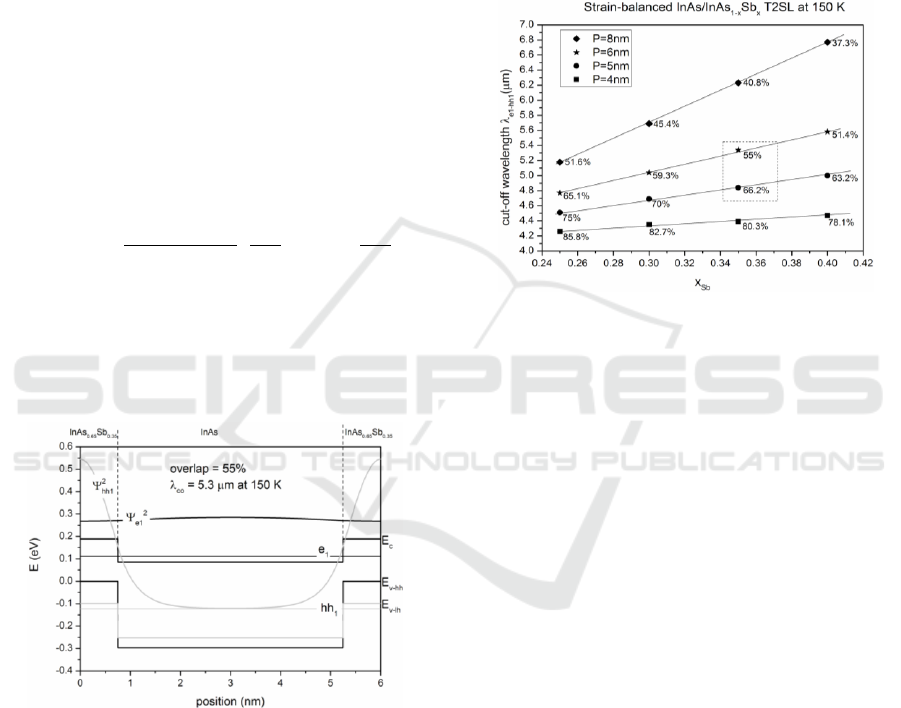
Figure 1: Band structure simulation of an InAs QW in
InAs
0.65
Sb
0.35
strain balanced on GaSb substrate with
periodic boundary conditions at 150 K. The dotted lines
are the 1st quantized energy levels of the electron confined
in the InAs layer and the heavy hole in InAsSb. Ψ
2
is also
plotted so that the zero of probability coincides with the
corresponding quantized energy level.
Assuming a type II-b InAs/InAsSb band offset (D.
Lackner et al., 2012) with electrons confined in the
InAs layer and holes confined in the InAsSb one
(Fig. 1), the quantized miniband energies of the
strain balanced InAs/InAs
1-x
Sb
x
T2SL were
calculated with nextnano
3
commercial software (See
http://www.nextnano.de/nextnano3/).
At T=150K, for x
Sb
varying from 0.25 to 0.4 and
P varying from 4 nm to 8 nm, cut-off wavelength
(λ
co
or λ
VH1-C1
) corresponding to ground heavy hole
VH1 to conduction C1 interminiband energetic
transition, is plotted on Fig. 2. For each case, wave
functions overlap |<Ψe
1
|Ψhh
1
>|
2
values calculated
for each fundamental VH1-C1 transition are also
specified.
Figure 2: Strain balanced InAs/InAs
1-x
Sb
x
T2SL on GaSb
substrate: Calculated cut-off wavelength at T = 150K and
associated wave functions overlap of the ground VH1-C1
miniband transition as a function of Sb concentration (x
Sb
)
and for different period thicknesses (P).
Consequently, to reach full MWIR detection, an
InAs/InAs
1-x
Sb
x
SL structure with x
Sb
= 0.35 and 5 ≤
P(nm) ≤ 6 could be of interest since numerical
simulations predict a cut-off wavelength between
4.8μm and 5.2μm and a wave functions overlap
between 55% and 66% (square with dashed lines
Fig. 2) at 150K.
3 MBE GROWTH
Ga-free InAs/InAsSb strain balanced SL lattice
matched to GaSb have been grown on n-type GaSb
Te-doped (100) substrates by solid source MBE
equipped with valved crackers set up to produce As
2
and Sb
2
species. Following the thermal oxide
desorption, a 400 nm-thick Te-doped GaSb buffer
layer was grown before the structure made of a 3μm
thick superlattice region composed of alternating
InAs(4.1 nm)/InAsSb(1.4 nm) non intentionally
doped (nid) layers and finally caped by a 150 nm-
thick n-doped Gasb layer (Fig. 3). Due to the well-
known competition for incorporation between
Arsenic (As) and Antimony (Sb) in the InAsSb
New Ga-Free InAs/InAsSb Superlattice Infrared Photodetector
233
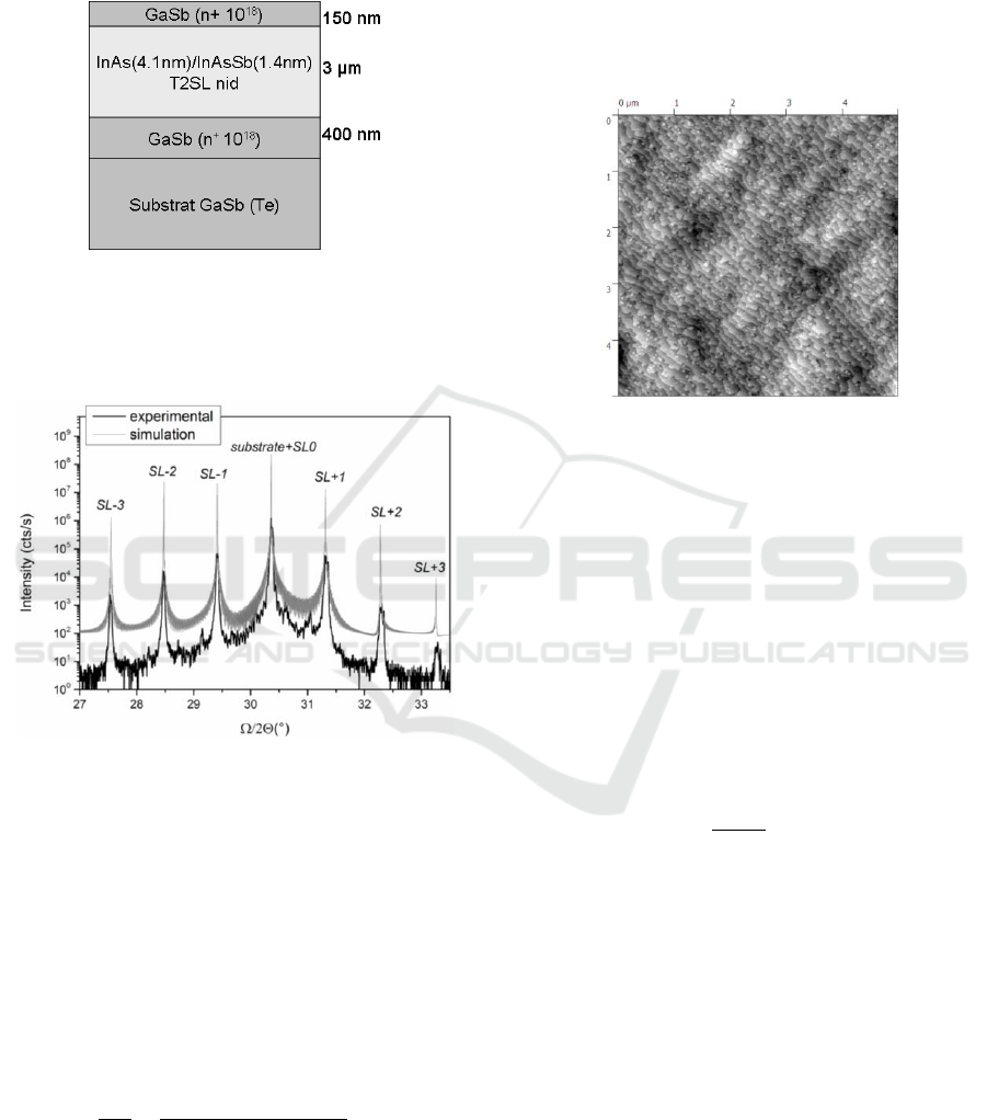
layer, several test samples have been grown to find
accurate speed growth of these species leading to
lattice-matched structure on GaSb with respect to x
Sb
= 0.35 in InAsSb layers.
Figure 3: InAs/InAs
1-x
Sb
x
T2SL sample cross-section.
The corresponding high-resolution X-ray diffraction
(XRD) spectrum shown in Fig. 4 exhibits many
intense satellite peaks with a full-width at half-
Figure 4: High-resolution XRD spectrum (004) reflection
of InAs/InAs
0.65
Sb
0.35
T2SL sample (P = 5.5nm) lattice-
matched to the GaSb substrate.
maximum (FWHM) of the first-order peak (SL0)
equals to 44 arcsec, attesting the good crystalline
quality of the layers. The targeted SL period value
(P = 5.5nm with layer thicknesses tInAs = 4.1 nm and
tInAsSb = 1.4nm calculated from Eqs (1) and (2)) is
confirmed by the simulated curve that matches the
experimental one.
In addition, the lattice mismatch calculated using
(T. Schuler-Sandy et al., 2015):
sin
1
sin ( )
substrate
substrate
a
a
(3)
where θ
substrate
is the angle in degrees of the substrate
peak measured by XRD and Δθ is the angular
difference between the substrate peak and the
epitaxial peak (the 0
th
order SL peak in this case) in
degrees is less than 300ppm.
The surface morphology has also been observed by
atomic force microscopy (AFM) on a 5x5μm
2
scan
area highlighting well-defined atomic steps (Fig. 5),
and measured root-mean-square (RMS) surface
roughness only equals to 0.15nm (that is, less than
one monolayer in the case of Sb-based materials).
Figure 5: AFM scan of InAs/In As
0.65
Sb
0.35
T2SL sample.
Clear monolayer steps can be observed.
4 OPTICAL
CHARACTERIZATIONS
The Ga-free InAs/InAsSb SL structure fabricated
could be the active zone of a XBn MWIR
photodetector. Such a device is designed to be
diffusion-current
1
limited. According to Eq. 4, the
diffusion-current is inversely proportional to the
minority carrier lifetime and the carrier
concentration Nd:
2
i
d diff
d
qn
JL
N
(4)
where q is the electrical charge, ni the intrinsic
carrier concentration and Ldiff the minority carrier
diffusion length. As a consequence, determination of
will give a trend on the expected dark current.
On top of this, it’s necessary to ensure that the SL
structure is suitable for the full MWIR domain. For
this purpose, photoluminescence (PL) measurements
allow to reach the bandgap energy of the structure,
which will correspond to the 50% cut-off energy of
the photodetector spectral response (see section 5.2).
4.1 Photoluminescence
Samples are placed in a cryostat allowing accurate
control of the temperature from 10K to 300K and are
PHOTOPTICS 2018 - 6th International Conference on Photonics, Optics and Laser Technology
234
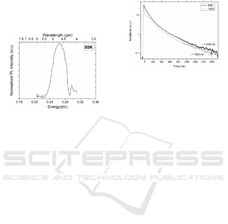
optically excited with a 50W/cm
2
power density
from a 784nm laser diode modulated at 133kHz
through a CaF
2
window. The luminescence signal is
analyzed with a Nexus 870 FT-IR system equipped
with a MCT detector (12µm cut-off wavelength).
Figure 6: PL spectra at T = 80K of a P = 6nm
InAs/InAs
0.65
Sb
0.35
SL sample.
Fig. 6 shows the normalized PL signal at 80K of a
InAs/InAs
0.65
Sb
0.35
SL structure with a 6 nm period.
The PL peak position, observed at wavelength equal
to 4.7µm at 80K, is in agreement with the calculated
fundamental valence to conduction interminiband
transition (Fig. 1). This result confirms the choice of
a T2SL period close to 6nm.
4.2 Photoluminescence Decay
To reach the minority carrier lifetime ,
photoluminescence decay (PLD) measurements have
been performed on structure presented in Fig. 3.
Among contactless techniques, this method remains
one of the simplest and most straightforward. The
experimental set-up used for PLD measurements is
the one described by Delacourt et al. (B. Delacourt
et al., 2017). Since excess carriers are generated by a
pulsed Erbium-doped fiber laser at a wavelength of
1545 nm, it’s important to note that, at this
wavelength, the light is absorbed by the active layer
while the heavily doped buffer and cap layers are
transparents. The PLD signals measured at 80K and
150K, for the same level of injection, are reported in
Fig. 7.
The time-resolved signal is then fitted by a least
squares Levenberg–Marquardt method
(B. Delacourt
et al., 2017) to estimate the contributions from
Auger (
Auger
), SRH (
SRH
) and radiative (
rad
)
recombinations to the total carrier lifetime, since:
1 1 1 1
()
Auger SRH rad
(5)
Figure 7: PLD signals of Ga-free sample at T=80K and
T=150K.
Values of 565ns and 605ns have been
respectively extracted at T=150K and T=80K,
highlighting a minority carrier lifetime for a Ga-free
InAs/InAs
0.65
Sb
0.35
SL around five times higher than
the InAs/GaSb SL’s one. It is to note here that
such values may certainly be improved since no
attempts to reach optimal growth conditions have
been performed. Moreover, investigation of the
different mechanisms (not presented in this work)
showed that the lifetime was clearly SRH limited.
5 GA-FREE SL IN XBN
CONFIGURATION
The XBn structure is composed of a n-type
absorbing layer (AL), an unipolar barrier layer (BL)
and a contact layer (CL). The objective of BL is to
block majority carrier (electrons) while allowing
collection of minority carrier (holes). When properly
designed, the use of a wide bandgap BL enables
device operation limited by diffusion current
1
.
5.1 XBn Architecture
The MWIR XBn detector is made of 3µm-thick Ga-
free InAs/InAs
0.65
Sb
0.35
AL, 80nm-thick n-doped
AlAs
0.09
Sb
0.91
BL and a 150nm-thick n+-doped
InAs
0.91
Sb
0.09
CL (Fig. 8).
XRD scan of the complete detector structure is
shown in Fig. 9. No angular difference Δθ~0 (Eq.3)
was detected between the substrate peak and the 0
th
order AL, indicating lattice-matching of this layer.
In contrast, the BL is in compressive strain with a
lattice mismatch around 2200ppm and a 94.5% Sb
composition in the AlAsSb ternary alloy. Anyway,
with a thickness of only 80nm, no relaxation occurs
in this layer. In addition, from satellite peak
New Ga-Free InAs/InAsSb Superlattice Infrared Photodetector
235
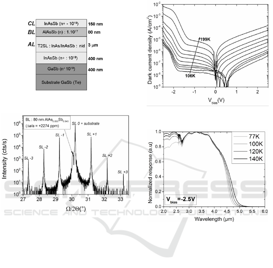
positions (SL-3, SL-2,.., SL+3) we can estimate the
period of the AL : P=5.3nm in that case.
Figure 8: Schematic cross-section of the XBn
photodetector
Figure 9: XRD spectrum (004) reflection of the complete
XBn structure (P = 5.3nm).
5.2 Experimental Results and Analysis
Standard optical photolithography was used to
define detector mesas varying in size from 60 μm
down to 310 μm in diameter. The mesas were etched
down to the GaSb layer with a citric acid/H2O2 based
etch solution (O. Dier et al., 2004). The diodes were
passivated by a thin SiO2 dielectric layer deposited
by plasma enhanced chemical vapor deposition
(PECVD). Dark current measurements (Fig. 10) as a
function of bias and temperature were then
conducted under vacuum within a liquid nitrogen
cooled Dewar.
The Ga-free SL XBn detectors operate under
negative bias voltages (negative voltage on the top
contact). The bias operation is extracted at -2.5V.
This too high value, necessary to allow the transport
of holes (minority carriers) from the AL to CL
through the BL clearly indicates that the valence
band alignment between the BL and AL is not
Figure 10: Dark current density vs bias at temperatures
between 106K and 199K for a 310μm diameter device.
Figure 11: Normalized spectral response measured at
different temperatures for a 310μm diameter device at
V
bias
=-2.5V.
optimized. Normalized spectral response
characteristics measured at different temperatures
for a 310μm diameter device at bias operation V
b
=-
2.5V are shown in Fig. 11.
From these measurements, we extract the cutoff
wavelength λ
co
= 4.6µm. This value, a bit lower than
the expected one, may probably be explained
because of a too short period of the SL (5.3nm
obtained vs 5.5 nm targeted).
6 PERFORMANCE
COMPARISON
From data presented in Fig. 10, we have plotted on a
Arrhenius graph (Fig. 12) the corresponding values
of the dark current density at V
bias
=-2.5V (red
PHOTOPTICS 2018 - 6th International Conference on Photonics, Optics and Laser Technology
236

circles) as a function of inverse temperature. In
addition, to compare the performances of our Ga-
free XBn device, we have also plotted in Fig. 12 the
data at bias operation of three different types of
InSb-based photodetectors (J. P. Perez et al., 2015)
(MWIR broadband detectors):
- InSb pn junction fabricated by standard planar
process,
- InSb pin junction fabricated by MBE,
- InSb nBn structure fabricated by MBE (A.
Evirgen et al., 2014).
The red line in Fig. 12 corresponds to the
diffusion regime of XBn structure. Consequently it
clearly appears that below 180K, our device is not
diffusion limited. Probably, due to its valence band
offset with the AL, AlAsSb is not the most
appropriate material for the BL. This is evidenced by
the large value bias operation we mentioned
previously in section 5.2. As a consequence, the
strong bias to be applied on our device to allow
holes (minority carriers) collection certainly leads to
tunnelling current contribution.
In Fig. 12, the horizontal dashed line indicates
the typical photonic current produced in the 3-5μm
band for f/3 optics by a III-V detector system with a
quantum efficiency = 80 % (M. A. Kinch et al.,
2010). On top of this, taking into account the criteria
according to which a high performance MWIR
detector must have a dark current density two
decades lower than its photocurrent (P. C. Klipstein
et al., 2004)), we also have reported in Fig. 12
the corresponding value (horizontal solid line):
6 10
-7
A/cm
2
.
Figure 12: Comparative Arrhenius plot of Ga-free SL with
three different types of MWIR broadband InSb-based
photodetectors.
Consequently, an optimized Ga-free SL structure in
XBn configuration should be able to operate at
temperature around 135K-140K, that is, a higher
temperature than InSb photodiode’s one operating in
the full MWIR spectral range.
ACKNOWLEDGEMENTS
Part of this work was supported by the French
“Investment for the future” program (Equipex
EXTRA ANR11-EQPX-0016).
REFERENCES
P. Klipstein et al., Opt Engin. 50, 061002 (2011).
A. Manissadjian et al., Proc. SPIE 8353, 835334 (2012).
Y. Reibel et al., Proc. SPIE 9451, 945110 (2015).
R. Taalat et al., J. Phys. D, Appl. Phys. 47 015101 (2014).
S. P. Svensson et al., J. Cryst. Gr., 334,103 (2011).
G. Chen et al., Opt. Lett. 40, 45 (2015).
N. Baril et al., Proc. of SPIE Vol. 10177 101771L-1,
(2017).
B. V. Olson et al., Appl. Phy. Lett. 101, 092109 (2012).
A. Haddadi et al., Appl. Phys. Lett. 106, 011104 (2015).
D. R. Rhiger et al., J. Electron. Mater. 45, 4646 (2016).
D. Lackner et al., J. Appl. Phy. 111, 034507 (2012).
See http://www.nextnano.de/nextnano3/ for more
information about the nextnano
3
software.
T. Schuler-Sandy et al., J. Cryst. Gr., 425, 29 (2015).
B. Delacourt et al., J. Elec.Mat. (2017) https://doi.org/
10.1007/s11664-017-5728-x.
O. Dier et al., Semicond. Sci. Technol., 19, 1250-1253,
(2004).
J. P. Perez et al., Proc. SPIE 9370 93700N-93700N-7
(2015)
A. Evirgen et al., Elec. Lett., 50, 20, 1472-1473, (2014)
M. A. Kinch et al., Proc. of SPIE, 7660, 76602V-1,
(2010).
P. C. Klipstein et al., Proc. of SPIE, 5406, 222-229 (2004).
New Ga-Free InAs/InAsSb Superlattice Infrared Photodetector
237
