
Transmission and Thermal Emission in the NO
2
and CO Absorption
Lines using Macroporous Silicon Photonic Crystals
with 700 Nm Pitch
D. Cardador, D. Segura, D. Vega and A. Rodríguez
Micro i Nanotecnologies, Departament d’Enginyeria Electrònica, Universitat Politècnica de Catalunya,
C/Jordi Girona, 31, 08031, Barcelona, Spain
Keywords: Photonic Crystals, Pitch, Cavity, Resonance, Transmission, Emission, Q-factor, Gas Sensor.
Abstract: Macroporous silicon photonic crystals with a cavity in the middle of their structure have been studied in
both, transmission and emission. The initial transmittance of the photonic crystals was increased form 4%-
6% up to the value of 25%-30% by performing a rear attach of the samples of approximately 160 µm. The
use of wafers with 700 nm of pitch allowed us to fabricate the optical response of the photonic crystals in
the ranges of 6.4 µm and 4.6 µm, where different gases have their absorption frequency –such as NO
2
or
CO. The fabricated samples have been also heated in order to evaluate their viability to be used as selective
emitters for gas sensing purposes. Results show a good agreement in the position of the respective peak
compared to the transmission spectrum. However, further studies have to be done to place the base of the
peak as close as possible to the 0% of emission in order to have a better selective emitter. This work is a
starting point for gas detection devices using macroporous technology in the mid-infrared, which includes
ammonia, formaldehyde, carbon monoxide or nitrous oxide, among others.
1 INTRODUCTION
Photonic Crystals (PC) are becoming increasingly
attractive for both research and market applications.
Their optical properties, obtained by creating
periodical structures of different refractive index
materials, are very interesting for a wide range of
application areas, such as optical communications or
sensing. The introduction of defects in the structure
that break the periodicity confers the PC some
interesting functionalities. They allow the creation of
resonant states within the photonic bandgap at
specific frequencies or modes -(Joannopoulos et al.
2011; Braun et al. 2006)- what can be used as
waveguides (Rinne et al. 2007), light couplers,
optical resonators (Youcef Mahmoud et al. 2012),
thermal emitters (Gesemann et al. 2010) or tuneable
filters (Neumann et al. 2008), etc.
As reported in the literature, there are several
factors that affect the photonic bandgap features:
the contrast between the high and the low reflective
index in the PC, the morphology, the light path,
etcetera (Joannopoulos et al. 2011). In the case of
introducing a defect inside the photonic crystal, it is
also important to have into account its shape to
predict the optical response of the structure. Several
articles have dealt with this issue in 1D and 2D PCs
–i.e. (Alvarado-Rodriguez 2003; Xiao et al. 2016;
Mohebbi 2015). However, the influence of the
defects morphology in the optical response of 3D
photonic crystals have not been so deeply analysed,
perhaps, because of the high dependence of the
method used to fabricate the PC (Nelson 2011;
Braun et al. 2006b). A number of different
techniques have been proposed to incorporate defect
structures within the PCs in woodpiles (Taverne et
al. 2015), synthetic opals (Massé et al. 2006;
Palacios-Lidón et al. 2004) or macroporous silicon
(Mertens et al. 2005), among others.
In this paper we focus on macroporous silicon
(mp-Si), which is a versatile material that can be
successfully fabricated through the so-called
electrochemical etching (EE). With this technique it
is possible to fabricate pores with different depth
profiles -such as sinusoidal or straight- with a planar
defect inside the crystal structure –see Fig. 1.
Previous studies reported mp-Si structures with a
cavity in the middle of the PC that had a resonant
wavelength around the 7 µm (Mertens et al. 2005).
Nevertheless, they worked with a lattice parameter –
Cardador D., Segura D., Vega D. and Rodrà guez A.
Transmission and Thermal Emission in the NO2 and CO Absorption Lines using Macroporous Silicon Photonic Crystals with 700 Nm Pitch.
DOI: 10.5220/0006120101910195
In Proceedings of the 5th International Conference on Photonics, Optics and Laser Technology (PHOTOPTICS 2017), pages 191-195
ISBN: 978-989-758-223-3
Copyright
c
2017 by SCITEPRESS – Science and Technology Publications, Lda. All rights reserved
191
also called pitch- of 2 µm and a vertical periodicity
about 2.5 µm. This vertical periodicity is limited to
the lattice parameter: when approaching to the pitch
value, the vertical periodicity is more difficult to
achieve and the profile is much more difficult to
control by EE. Although some other studies reported
modulated structures in 700 nm (Langner 2008),
they did not insert a cavity in their structures,
probably because the profiles were not as good as
the ones obtained in 2 µm of pitch. In the present
study, the samples used to fabricate the macroporous
silicon PCs had a pitch of 700 nm and a vertical
periodicity around the lattice parameter, what
enabled us to place a peak and tailor it at wavelength
as short as 4.6 microns, were different gas
absorption peaks can be found.
By removing around 160 µm of bulk silicon of the
samples, we have been able to increase the
transmission percentage from values around 4%-6%
up to values between 25% and 30%. This improves
the features of the peak –i.e. transmittance and
quality factor- and, as a consequence, the sensitivity
of the final gas sensor device is enhanced. Further
improvement of the transmission could be achieved
by removing some more bulk silicon, but the risk of
damaging the photonic crystal –mechanical support
or etching of the PC structure- becomes high and
some silicon bulk has to be left to avoid these
problems. In the case of thermal emission this layer
has not an important impact in the relative
transmission amplitude of the peak –from the base to
the top of the resonant peak-, but it has a
considerable effect in the position of the base point.
Specifically, the more bulk silicon the more
radiation of the no texturized region, which is finally
reflected in a higher offset from the zero emission
point to the base point, where the emission peak
rises.
The conclusions drawn in this paper lead us to
confirm that the studied macroporous silicon
structures can be employed in gas sensing
applications. However, further work has to be done
in order to improve the amplitude and the Q-factor
of the peak, as well as to reduce the offset, either
working in transmission or emission.
2 EXPERIMENTAL
The 3D structures were obtained by electrochemical
etching of n-type (100) crystalline silicon samples in
hydrofluoric (HF) acid solution. The starting
material had a resistivity between 0.1-0.3 Ω·cm
(~3·10
16
/cm
3
phosporous-doped). An N
+
layer was
implanted on the backside of the wafer to provide a
low-resistance transparent ohmic contact. Next, the
wafer was oxidized and a nanoimprint lithography of
700 nm pitch was performed. A Reactive-ion
Etching (RIE) and a tetramethylammonium
hydroxide (TMAH) etching were done to create
inverted pyramid-shaped pits that act as nucleation
centres for the ordered pore growth. Finally, the EE
etching was carried out to control the modulation of
pore diameter which, is regulated by the applied
etching current. This method allows to design the
profile beforehand and to create smooth 3D
structures of great complexity just by applying
different etching currents.
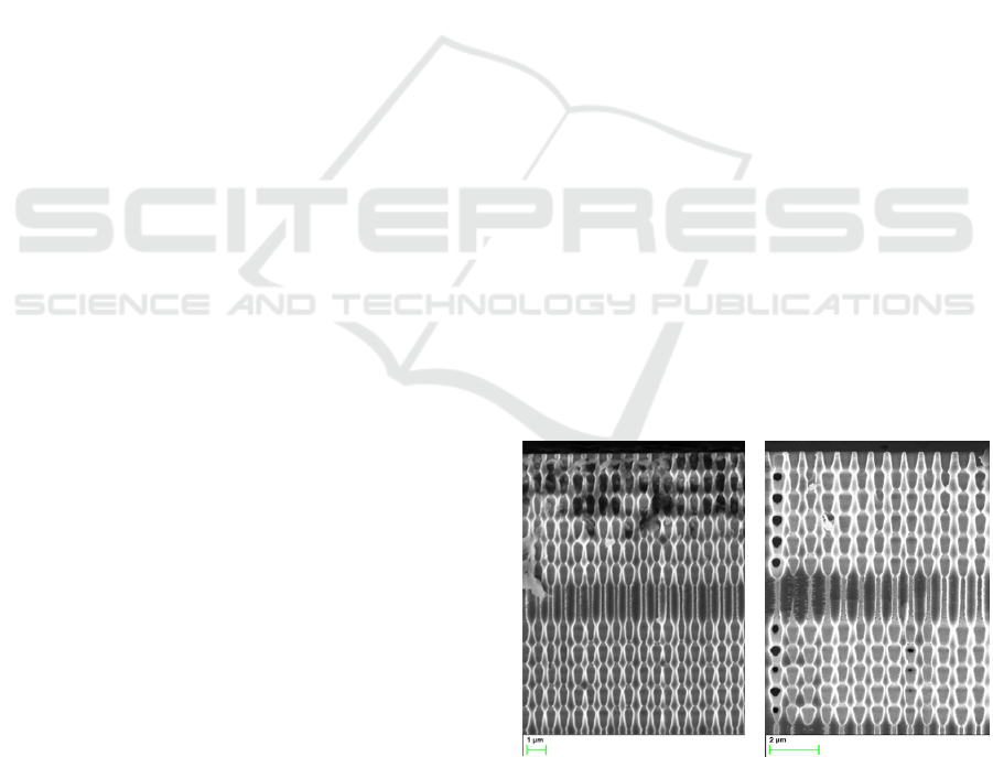
In particular, the periodical profiles attached in
Fig.1 have been generated. In the first sample (left)
the depth periodicity was set to be about 1.1-1.2 µm
what arouse a bandgap around [5-7] µm. As
depicted in the figure, a planar defect was introduced
halfway the total pore depth by suppressing one of
the modulations and leaving a constant diameter
section. The length of the cavity varied from 2.1 µm
to 2.6 µm with a diameter of 0.23 µm in all the
samples. In order to reduce the bandgap central
wavelength, and thus the position of the peak, the
vertical modulation of the pore was shortened. In
concrete, it was set to the lattice constant value
(~700nm). Thanks to that, the bandgap moved to the
range of [4-5] µm, while the defect’s length took
values in the range of [1.5-1.8] µm. The total depth
of all samples was about 12-15 micrometers. A
complete description of the process can be found
elsewhere (Lehmann 1993). The second fabricated
structure can be observed in the right image.
Figure 1: Cross sectional view of two 3-D PCs fabricated
by EE over a litography of 0.7 μm pitch. The inclusion of
a defect in the PC lattice enables a transmitted mode in 6.4
µm (left) and 4.6 µm (right). (les he reordenat en l’ordre
del text).
PHOTOPTICS 2017 - 5th International Conference on Photonics, Optics and Laser Technology
192
The transmitted response of the fabricated samples
was measured in the MIR range using a Bruker
Optic’s Vertex FT-IR spectrometer. The lattice was
aligned to the Γ – M direction (along one lattice axis
in the surface), an aperture of 1 mm and a resolution
of 4 cm
-1
was used for the calculation of the
spectrum. The measurements have been referred to
the source spectrum to normalize the results.
The emissivity was experimentally measured
using the A540 emission adapter of the FT-IR
spectrometer. This commercial setup allows normal
thermal emission measurement, with a beam
opening angle of ±7,5°, from room temperature up
to 400 °C. In this setup, the sample is clamped
vertically to a metallic surface that is at a constant
temperature. After thermalization, the sample is at a
constant and homogeneous temperature very close to
the temperature of the heater, since c-Si is an
excellent thermal conductor. In our case, the samples
were heated at the highest possible temperature in
order to obtain the maximum power of the emitter.
Finally, the emissivity values are obtained after
conducting a standard calibration with a piece of
polished Si as reference.
3 RESULTS AND DISCUSSIONS
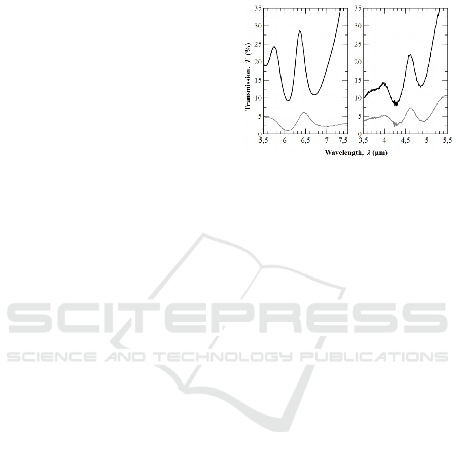
The two fabricated samples of the Figure 1: are
characterized in the FT-IR. In the Figure 2: the
sample’s transmission spectrum is shown. As
depicted in it, there is a high enhancement in the
transmission due to the reduction of, approximately,
160 µm of bulk silicon from the back side of the
wafer. In particular, the transmission percentage
rises from the value of 6% up to 29%. Previous
studies reported maximal transmission peaks of
almost 50% using mp-Si structures. Nonetheless,
their peaks were placed out of the mid-infrared
range –following the same convention as in (Byrnes
2008)- in concrete at 20 µm, far from the interesting
gas sensing mid infrared frequencies.
Figure 2: Transmittance of the samples before (grey) and
after (black) the TMAH attack for removing part of the
bulk silicon of the wafer. The different wavelength range
are achieved by controlling the vertically periodicity. Left
image corresponds to the image plotted in Fig.1(a) and the
right image to the Fig.1(b).
The values presented in this work are the best
ones reported in the mid-infrared, as far as our
research reached, in 3D mp-Si structures. Moreover,
the use of samples with 700 nm of pitch made
possible to reduce the vertical modulation and adjust
its periodicity close to the lattice constant. This
entailed a proportional translation of the entire
spectrum towards lower frequencies. An
appropriated dimensioning of the defect’s length and
width lead us to correctly place a resonant mode
inside the bandgap. Consequently, we were able to
reproduce the transmittance figure around 4.6 µm,
where the CO has its absorption lines –see Fig. 2.
As explained in the introduction, below the PC
there is some remaining bulk silicon. This silicon
reduces the amount of ideally transmitted light,
which in simulations –without any bulk silicon- can
be around 60%. However the reduction of more
silicon presents some problems. The first of them is
the risk of damaging the PC structure after some
hours of TMAH attack. The second one is that if the
attacked surface is big, some mechanical stress can
appear, completely breaking the surface as a
consequence.
One interesting fact is that by removing some
bulk silicon the quality factor of the peak is also
enhanced, improving the performance of a future gas
sensor. Nevertheless, the transmission inside the
band gap is also increased what, in turn, will result
in less sensitivity in a gas sensor. Some research
should be carried out to reduce the transmission
inside the band gap for obtaining good gas sensors.
Transmission and Thermal Emission in the NO2 and CO Absorption Lines using Macroporous Silicon Photonic Crystals with 700 Nm Pitch
193
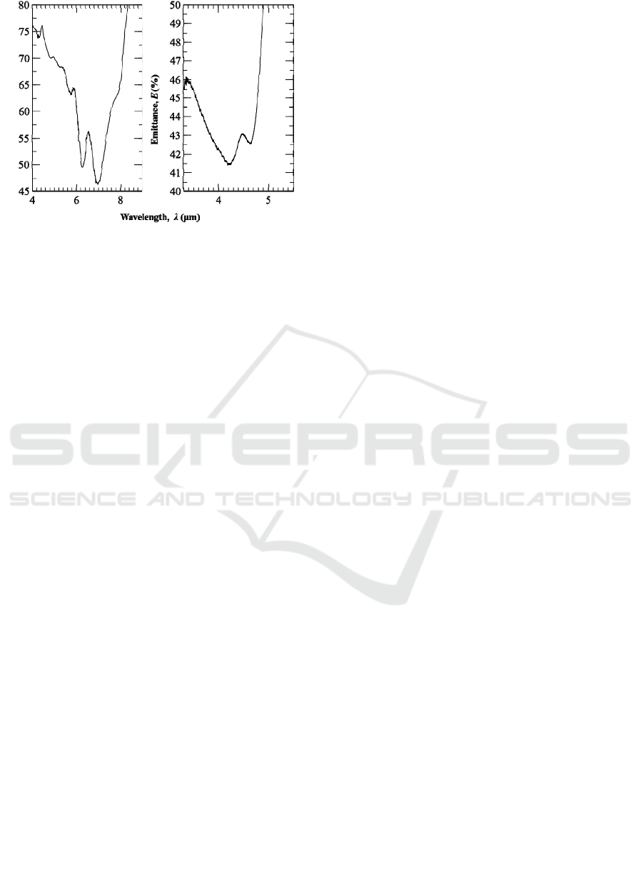
Figure 3: Experimental emisison spectra for the samples
depicted in Fig. 1 (they are conveniently depicted. E.g.:
left image in Fig. 1 corresponds to the left image in Fig.3).
Both samples were heated at 400 ºC.
In the right image of the Fig. 2, it can be seen the
trademark of the CO
2
absorption lines at a 4.25 µm
wavelength. These marks correspond to variations of
gas concentrations referred to the background case.
If the peak is positioned on the absorption lines of a
target gas, the concentration of it can be determined
by comparing the area of the peak before and after
the gas exposure. Even more, despite using the PC
for filtering the light coming from the emitter, the
sample can be heated in order to have an emission
peak at the desired wavelengths. This would allow
replacing the optical emitter for a selective thermal
emitter, emitting in a smaller range of wavelengths,
and thus, simplifying the configuration for sensing
gases, probably without the need of an optical filter.
The lowered samples were used to evaluate their
thermal emission in the two studied wavelengths –
see Fig. 3- when the samples are heated at 400ºC.
The peaks are placed around 6.5 µm and 4.5 µm, in
good accordance with the position of the peak in
transmission. If observed insightfully a peak
broadening of about 100 nm can be seen in both
cases. A reduction of their respective amplitudes,
compared to their transmission spectrum, is also
noticeable, particularly at 4.5 µm. During the study
we have verified that there are some variations in the
pore’s morphology due to the expansion of the
silicon with the heating of the sample, which affects
the optical response of the peak; these experimental
variations, although they are of a few tens of
nanometers, modify the local refractive index what,
finally, impacts in the position and the amplitude of
the peak.
Another remarkable point is that the peaks do
not start at zero position; they have their beginning
at the emissivity of 40%-45%. Probably part of this
offset is due to the remaining bulk silicon in the
bottom of the photonic crystal, which also radiates in
the frequencies of the peak, reducing the
performance of the samples as selective thermal
emitters.
Further studies should deal with this issue in
order to obtain good selective emitters that
propagate a range of frequencies along its bandgap.
4 CONCLUSIONS
Macroporous silicon photonic crystals with a defect
inserted in the middle of the structure have been
studied. The initial transmittance of these structures
is between the 4% and the 6%. Performing a rear
attach of the sample –approximately 160 µm-, the
transmission percentage increases to the value of
25%-30%.
The use of samples with 700 nm of pitch allows
to work with sub micrometre vertical periods.
Thanks to this, peaks at lower resonant frequencies
can be placed, in concrete, we have fabricated two of
them: at 6.4 µm and 4.6 µm, what can be used to
sense different gases that have their absorption
frequency in ranges close to that values –such as
NO
2
or CO.
Both peaks been heated at room temperature of
400 ºC in order to obtain a selective emitter. Results
show a good agreement in the position of the peak
compared to the position in the transmission
spectrum. The little differences are attributable to
the variations in the shape of the pores given by the
expansion of the silicon due to higher temperatures.
Further studies have to be done to place the base of
the peak as close as possible to the 0% of emission
in order to have a real selective emitter.
This work is a starting point for gas detection
devices using macroporous technology in the mid-
infrared, which includes ammonia, formaldehyde,
carbon monoxide or nitrous oxide, among others.
ACKNOWLEDGEMENTS
This work has been founded by TEC-2013-48-147-
C6-2-R.
REFERENCES
Alvarado-Rodriguez, I., 2003. Fabrication of two-
dimensional photonic crystal single-defect cavities and
their characterization by elastic scattering. A
PHOTOPTICS 2017 - 5th International Conference on Photonics, Optics and Laser Technology
194

dissertation Doctor of philosophy in Electrical
Engineering.-Los Angeles, University of california.
Braun, P.V., Rinne, S.A. & García-Santamaría, F., 2006.
Introducing Defects in 3D Photonic Crystals: State of
the Art. Advanced Materials, 18(20), pp.2665–2678.
Byrnes, J., 2008. Unexploded ordnance detection and
mitigation. Springer Science & Business Media.
Gesemann, B., Schweizer, S.L. & Wehrspohn, R.B., 2010.
Thermal emission properties of 2D and 3D silicon
photonic crystals. Photonics and Nanostructures -
Fundamentals and Applications, 8(2), pp.107–111.
Joannopoulos, J.D. et al., 2011. Photonic Crystals:
Molding the Flow of Light, Princeton university press
(Second Edition).
Langner, A., 2008. Fabrication and characterization of
macroporous silicon. Doktorarbeit, Martin-Luther-
Universität.
Lehmann, V., 1993. The Physics of Macropore Formation
in Low Doped n-Type Silicon. Journal of The
Electrochemical Society, 140(10), p.2836.
Massé, P. et al., 2006. Tailoring planar defect in three-
dimensional colloidal crystals. Chemical Physics
Letters, 422(1-3), pp.251–255.
Mertens, G. et al., 2005. Tunable defect mode in a three-
dimensional photonic crystal. Applied Physics Letters,
87(24), p.241108.
Mohebbi, M., 2015. Refractive index sensing of gases
based on a one-dimensional photonic crystal
nanocavity. Journal of Sensors and Sensor Systems.
Nelson, E., 2011. Three-dimensional photonic crystal
optoelectronics. Diss. University of Illinois at Urbana-
Champaign.
Neumann, N. et al., 2008. Tunable infrared detector with
integrated micromachined Fabry-Perot filter. Journal
of Micro/Nanolithography, MEMS and MOEMS, 7(2),
p.021004.
Palacios-Lidón, E. et al., 2004. Engineered Planar Defects
Embedded in Opals. Advanced Materials, 16(4),
pp.341–345.
Rinne, S.A., García-Santamaría, F. & Braun, P. V., 2007.
Embedded cavities and waveguides in three-
dimensional silicon photonic crystals. Nature
Photonics, 2(1), pp.52–56.
Taverne, M., Ho, Y. & Rarity, J., 2015. Investigation of
defect cavities formed in three-dimensional woodpile
photonic crystals. JOSA B.
Xiao, X. et al., 2016. Investigation of defect modes with
Al2O3 and TiO2 in one-dimensional photonic crystals.
Optik - International Journal for Light and Electron
Optics, 127(1), pp.135–138.
Youcef Mahmoud, M. et al., 2012. Optical channel drop
filters based on photonic crystal ring resonators.
Optics Communications, 285(3), pp.368–372.
Transmission and Thermal Emission in the NO2 and CO Absorption Lines using Macroporous Silicon Photonic Crystals with 700 Nm Pitch
195
