An Electro-optical Connectome Prototype for Eight Neuron
Representations in FPGA Technology
Lorenzo Ferrara, Alexey Petrushin and Axel Blau
Dept. of Neuroscience and Brain Technologies (NBT), Italian Institute of Technology (IIT), 16163 Genoa, Italy
Keywords: Brain-inspired Computation, Nervous System Emulation, Optical Connectome, Parallel Information Flow,
Structured Illumination, Replica-casting, Field-programmable Gate Arrays.
Abstract: In nature, interneural signaling is highly parallel and temporally precisely structured. It would require equal
parallelism and temporal accuracy to faithfully mimic neural communication in hardware representations.
Light-based communication schemes fulfil this prerequisite. We report on a prototype of an optical
connectome implementation for a neuromorphic system eventually consisting of eight neurons. The
platform is based on field-programmable gate arrays (FPGAs) that run neuron-specific response models.
Their axons are represented by light-emitting diodes (LEDs) with axonal arbors in the form of micro-
patterned transparencies. They distribute membrane voltage threshold crossings, which are represented by
light pulses, onto synapse-specific photodiodes of postsynaptic neurons. This contribution sketches out the
overall system design and discusses its prospective application in replicating the connectome of the
nematode C. elegans in the framework of the Si elegans project.
1 INTRODUCTION
Surprisingly, even simple biological neural
networks can outperform today’s fastest
computational systems in tasks such as pattern
recognition and locomotion control. Nervous
systems are complex, highly parallel information
processing architectures made of seemingly
imperfect and slow, yet exceptionally adaptive and
power-efficient components to carry out
sophisticated information processing functions.
However, despite the rapidly growing body of
knowledge on almost every aspect of neural
function, currently no computational model or
hardware emulation exists that is able to describe
or even reproduce the complete behavioural
repertoire of the nematode Caenorhabditis elegans,
an organism with one of the simplest known nervous
systems. C. elegans, a soil-dwelling worm with a life
span of a few days, 1 mm long and 80 µm in
diameter, is one of the five best characterized
organisms. It is multicellular and develops from a
fertilized egg to an adult worm similar to higher
organisms. The morphology, arrangement and
connectivity of each cell including its neurons
have been completely described
and are found to
be almost invariant across different individuals.
Initially, 6393 chemical synaptic connections, 890
electrical junctions, and 1410 neuromuscular
junctions were identified (White et al., 1986). Recent
revisions of the original electron microscopy datasets
suggest that these numbers may actually be higher.
All of this data including the connectome, the
detailed interconnectivity map of the 302 neurons
through synapses, is publicly available through the
Worm Atlas (Achacoso and Yamamoto, 1992;
Oshio et al., 2003; Varshney et al., 2011). Despite its
simplicity, the nervous system of C. elegans does
not only sustain vital body function, but generates
a rich variety of behavioural patterns in response
to internal and external stimuli. These include
associative and several forms of nonassociative
learning that persist over several hours (Hobert,
2003). Interestingly, many processes of learning and
memory in C. elegans were highly conserved across
different species during evolution, which
demonstrates that there are universal mechanisms
underlying learning and memory throughout the
animal kingdom (Lin and Rankin, 2010).
To replicate the parallel information processing
pathways in nervous systems as faithfully as
possible, an equally parallel information
Ferrara, L., Petrushin, A. and Blau, A..
An Electro-optical Connectome Prototype for Eight Neuron Representations in FPGA Technology.
In Proceedings of the 3rd International Congress on Neurotechnology, Electronics and Informatics (NEUROTECHNIX 2015), pages 127-132
ISBN: 978-989-758-161-8
Copyright
c
2015 by SCITEPRESS – Science and Technology Publications, Lda. All rights reserved
127
transmission scheme would be required. However,
classical 2D interconnectivity designs are based on
serial data transmission protocols, which are prone
to temporal jitter when simultaneously distributing
signals to more than one target receiver. Parallel
wire-based approaches will likely encounter
interconnect bottlenecks upon their upscaling to the
simultaneous addressing of a high number of target
synapses (Cangellaris, 1998). The Si elegans project
therefore pursues the development and
implementation of a 3D electro-optical free-space
interconnectivity scheme for the parallel
transmission and precise temporal processing of
neuronal information. The general concept and its
variants have been sketched out and discussed in
previous publications (Petrushin et al., 2014;
Petrushin et al., 2015).
In this contribution, we report on the elements
and working principle of an 8-neuron prototype of a
static light-based connectome and its integration
with the FPGA representations of their pre- and
postsynaptic neurons.
2 OPTICAL EMITTER AND
LIGHT DISTRIBUTION
ELEMENTS
Membrane potential threshold crossings of nerve
cells, here represented by field-programmable gate
array (FPGA) boards, are transmitted from pre- to
postsynaptic neurons by an optical connectome.
When the neural response model in a presynaptic
FPGA reaches that threshold, it sets its axonal
output, one of its freely addressable I/O pins, to a
high state. This triggers the light source, thereby
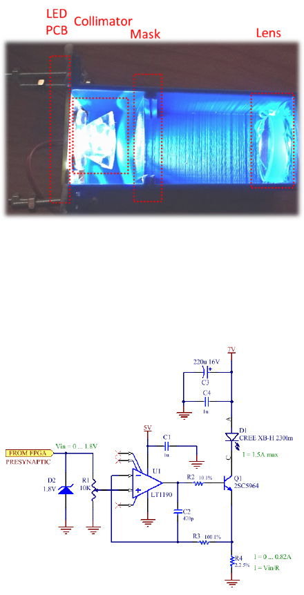
initiating the optical communication. The light-
emitter module is composed of a printed circuit
board (PCB) with a light-emitting diode (LED) and
its driver, a collimator in front of the LED to reduce
the divergence of the beam, a transparent mask that
structures the projected light into permissive and
non-permissive pathways, a lens that focuses the
mask pattern on the target and a box to contain all of
these elements (
Figure
1).
An XLamp® XB-H LED was selected as the
light source. This LED has sufficient light intensity
(230 lm). Its emitted color matches the spectral
sensitivity of the photodetector. An LED was
preferred to a laser diode for its longer lifetime and
lower cost. The LED modulator is shown in Figure
2. It works as follows: the input voltage, V
in
, appears
at the non-inverting input of the operational
amplifier (op-amp) U1. U1 forms a feedback loop
that drives the transistor Q1 in such way that the
voltage at the current-limiting resistor R4 is equal to
V
in
. The input voltage can range from 0 to 1.8 V.
Figure 1: Light-emitter module.
At 0 V, the LED turns off. At 1.8 V, the LED turns
on and draws a maximum current of 0.82 A. The
trimmer, R1, is used for adjusting the light intensity.
Additional resistors and capacitors were added for
stability purposes.
Figure 2: LED modulator schematics.
The collimator is an ASMT-M015 component
(Avago). It is glued in front of the LED to collimate
the light to an angle of 15 °, thereby concentrating
the light and reducing optical losses.
The light-distribution mask is composed of a
transparency film, which is printed with black toner
from a laser printer and then cut to fit the box. The
mask is patterned to project the light only on the
target photodiodes of those postsynaptic FPGA
neurons that a presynaptic neuron establishes
connections with.
NeBICA 2015 - Symposium on Neuro-Bio-Inspired Computation and Architectures
128
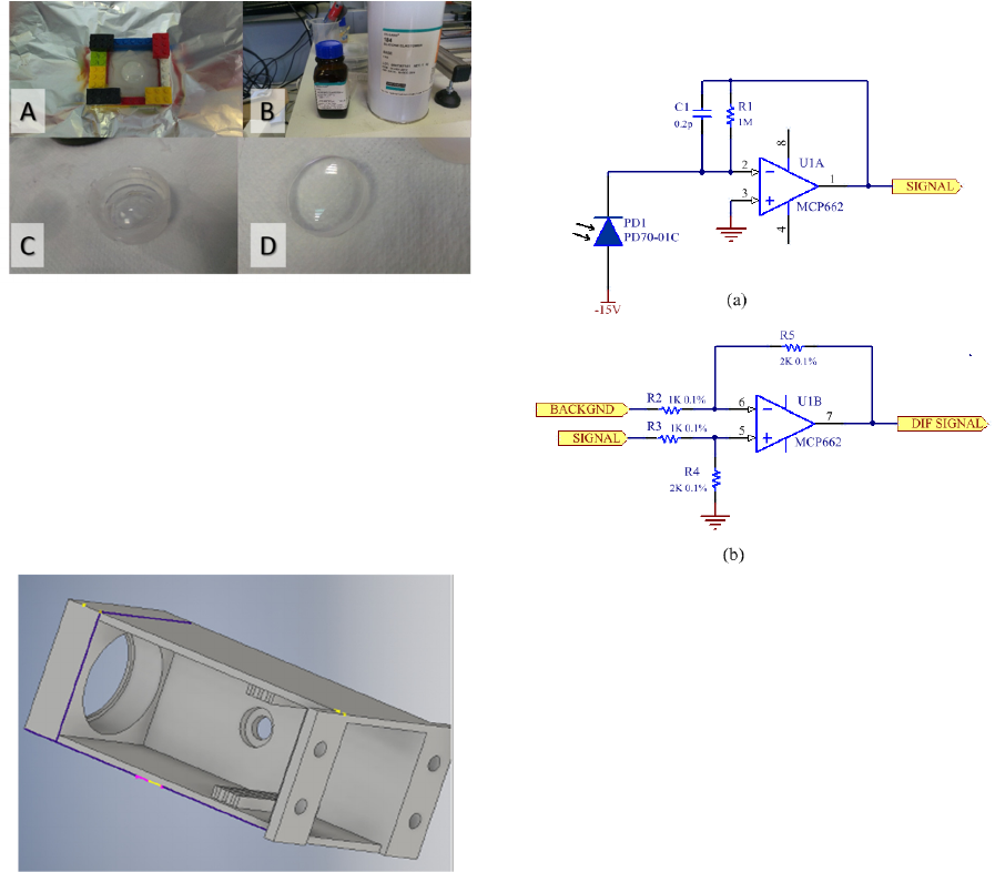
The lenses are plastic replica of a plano-convex
lens with a diameter and focus of 25 mm. The
fabrication process (
Figure 3
) consists of creating a
polydimethylsiloxane (PDMS) mold of the original
lens with clay (A), filling the mold with a
photoresist (SU8, MicroChem; B and C) with the
desired optical characteristics (e.g., refractive index)
and curing it to give a replica-lens (D). This strategy
results in affordable lenses of good optical quality.
Figure 3: Replica-molding of lenses.
The housing for the optical elements is made from
acrylonitrile butadiene styrene (ABS) by resorting to
a 3D printing technique. The computer-aided design
(CAD) (Figure 4) features holes for attaching the
PCB, a hole for the fixation of the module mounting
column and its alignment, the correct focal distance
between the mask and the lens, a support structure
for the mask and an aperture for the lens.
Figure 4: CAD view of the housing of the light-emitter
components.
3 PHOTORECEIVER AND
SIGNAL CONDITIONING
ELEMENTS
The optical signals are converted into electrical
signals by a photodiode (Everlight, PD70-01C). This
opto-electrical transducer was selected for its small
footprint, good sensitivity, high efficiency in the
visible spectrum and its relatively small parasitic
capacitance. Once light strikes the active area of the
photodiode, a current flows from the cathode to the
anode. The generated current is on the order of
microamperes and needs to be amplified before it
can be processed by subsequent electronics. This
amplification is performed by a current-to-voltage
converter configuration called transimpedance
amplifier (Figure 5).
Figure 5: A) Transimpedance Amplifier Schematics. B)
Differential Amplifier Schematics.
The negative input of the amplifier, U1A, senses
the current generated by the photodiode. Voltage on
the output of the amplifier will be equal to the
photocurrent times the value of the feedback
resistor, R1. A small feedback capacitor, C1, is
necessary to maintain stability. The photodiode is
operated in photoconductive mode with a -15 V
reverse bias voltage. The advantage of such biasing
is an increase of the system’s dynamic range. As a
drawback, biasing will result in a higher dark
current. However, this increase in the dark current is
not critical for the application. The transimpedance
op-amp should have a large gain bandwidth, a low
input capacitance and a low bias current. In addition,
it should come in a dual op-amp surface mounted
device (SMD) package with a small footprint,
feature a rail-to-rail output and operate on a power
supply as low as 3.3 V. Among the available op-
amps, the model MCP662 (Microchip) was selected.
An Electro-optical Connectome Prototype for Eight Neuron Representations in FPGA Technology
129
The illumination pattern is defined by a mask
with black and transparent regions. Ideally, the black
areas of the mask should block the light completely.
However, in practice, some light passes through the
black areas of the mask, thereby creating some
background illumination. In order to separate the
signal from the background, one of the photodiodes
is used as a background reference sensor. This
photodiode generates a background level signal,
which is subtracted from the received signal. This
operation is performed by the differential amplifier,
U1B (Figure 5). The obtained differential signal is
compared to the reference voltage of 1.1 V (Figure 6).
Figure 6: Comparator schematics.
If the reference voltage is higher than the signal, the
output of the comparator, U2A, stays low. If the
reference voltage is lower than the differential
signal, the output of the comparator, U2A, changes
to high. The comparator output is connected to the
respective pin of the postsynaptic FPGA. Resistors
R9 and R10 were added to suppress any undesired
toggling of the output. The termination resistor, R5,
dampens any over- or undershoot to increase the
signal quality.
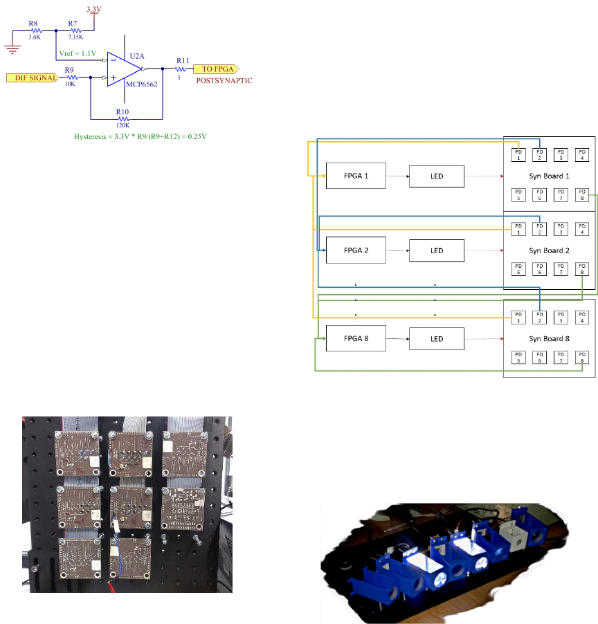
In this work, we installed a synaptic panel
composed of 8 synaptic boards (SBs), each carrying
the driving circuitry for 8 photodiodes (Figure 7).
The relative position of the photodiodes with
Figure 7: Synaptic panel with 8 synaptic boards. Each SB
controls 8 photodiodes. In the figure, only 4 SBs are fully
populated.
respect to each other equals their dimensions
(approximately 8 x 8 mm
2
). The pitch and the active
area of the photodiodes define the mask structure
because the projected light from an LED has to shine
on the correct postsynaptic target photodiodes, but
avoid those that do not participate in a particular
synaptic connection configuration.
4 INTEGRATION WITH THE
FPGA HARDWARE
INFRASTRUCTURE
To test the connection, the optical connectome was
integrated with remotely controlled FPGA boards.
Each board (Terasic, Altera DE4) drove a single
axonal LED as a pre-synaptic neuron and received
the output from one of the photodetectors on each
SB when acting as a postsynaptic neuron. A simple
connectome scheme is depicted in
Figure
8.
Figure 8: Schematics of the neural connectome. For
simplicity, only 3 out of 8 neurons are depicted.
Eight light-emitter modules were aligned to shine
their light patterns onto the synaptic panel, each
carrying a different mask for a neuron-specific
projection scheme (Figure 9).
Figure 9: Eight light-emitter modules of an 8-neuron
communication connectome.
NeBICA 2015 - Symposium on Neuro-Bio-Inspired Computation and Architectures
130
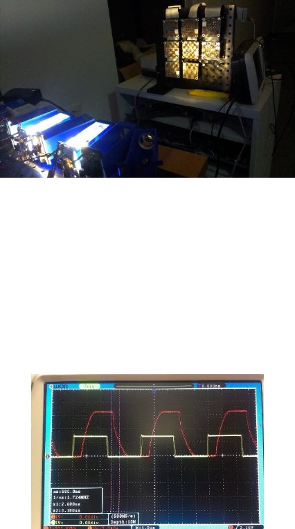
In one validation experiment, four FPGAs were
activated to simulate the communication between
four neurons. Figure 10 demonstrates the projection
through two masks of two firing LEDs.
Figure 10: Test projection of two LED illumination
patterns driven by their respective pre-synaptic FPGAs.
The test was performed at different frequencies to
evaluate the delay between the triggering signal
from the FPGA and the response of the targeted
photodiode (yellow and red traces in Figure 11,
respectively). The response with a delay of 500 ns
and a maximum operation frequency of 200 kHz is
sufficiently accurate and fast to emulate biological
spiking.
Figure 11: PD response to an LED illumination. The
maximum modulation frequency that keeps a 50% duty
cycle is around 200 kHz.
5 CONCLUSIONS
A parallel electro-optical setup that faithfully
mimics neural communication and its timing has
been implemented. Although the hardware is
currently limited to the emulation of 8 neurons, it
demonstrates the proof of principle for the emulation
of more complex neural networks such as the
complete connectome of the nematode C. elegans
(302 neurons, ~8,000 connections). A platform
based on FPGAs has sufficiently extensive
computation capability for the emulation of very
complex neural response algorithms and network
connectivities. To date, proof-of-concept tests have
been performed to demonstrate the correct synaptic
connection through precise light addressing. The
setup will be employed to further investigate
phototaxis in C. elegans, where 8 neurons are
involved.
ACKNOWLEDGEMENTS
The Si elegans project 601215 is funded by the 7
th
Framework Programme (FP7) of the European
Union under FET Proactive, call ICT-2011.9.11:
Neuro-Bio-Inspired Systems (NBIS). Kind loans of
electronic equipment by the IIT robotics workshop
team were very much appreciated. Many thanks to
our collaboration partners Martin McGinnity, Pedro
Machado, Alicia Costalago Meruelo and Kofi
Appiah for their help and fruitful discussions. We
are very grateful for FPGA board donations by
Altera.
REFERENCES
Achacoso, & Yamamoto. (1992). AY's Neuroanatomy of
C. elegans for Computation (pp. 304): CRS Press,
Boca Raton, FL.
Cangellaris. (1998). The interconnect bottleneck in multi-
GHz processors; new opportunities for hybrid
electrical/optical solutions. Fifth International
Conference on Massively Parallel Processing, Las
Vegas, Nevada, USA.
Hobert. (2003). Behavioral plasticity in C. elegans:
Paradigms, circuits, genes. Journal of Neurobiology,
54(1), 203-223.
Lin, & Rankin. (2010). Nematode Learning and Memory:
Neuroethology. In Breed & Moore (Eds.),
Encyclopedia of Animal Behavior (pp. 520-526).
Oxford: Academic Press.
Oshio, Iwasaki, Morita, et al. (2003). Database of
Synaptic Connectivity of C. elegans for Computation.
Retrieved from http://ims.dse.ibaraki.ac.jp/ccep/.
Petrushin, Ferrara, & Blau. (2015). The Si elegans
connectome: A neuromimetic emulation of neural
signal transfer with DMD-structured light. SPIE
Photonics West, Emerging Digital Micromirror
Device Based Systems and Applications VII, Session
6: Novel and Emerging DMD Applications, San
Francisco, USA.
Petrushin, Ferrara, Liberale, et al. (2014). Towards an
electro-optical emulation of the C. elegans
connectome. 2nd International Congress on
Neurotechnology, Electronics and Informatics, Rome,
Italy.
An Electro-optical Connectome Prototype for Eight Neuron Representations in FPGA Technology
131
Varshney, Chen, Paniagua, et al. (2011). Structural
Properties of the Caenorhabditis elegans Neuronal
Network. PLoS Computational Biology, 7(2),
e1001066.
White, Southgate, Thomson, et al. (1986). The Structure
of the Nervous System of the Nematode
Caenorhabditis elegans. Philosophical Transactions
of the Royal Society of London. B, Biological Sciences,
314(1165), 1-340.
NeBICA 2015 - Symposium on Neuro-Bio-Inspired Computation and Architectures
132
