
High Performance Silicon-on-Sapphire Subwavelength Grating
Coupler for 2.7μm Wavelength
Jingjing Zhang, Junbo Yang, Wenjun Wu, Honghui Jia and Shengli Chang
Center of Material Science, National University of Defense Technology, Changsha 410073, China
Keywords: Beam Splitter, Grating-Assisted Coupler, Coupled Mode Theory, Transfer Matrix Method.
Abstract: Couplers are important parts in integrated optical circuit and high efficiency compact couplers are in great
demand. We report on high-efficiency silicon-on-sapphire (SOS) grating couplers at wavelength of 2.7μm.
A 75% coupling efficiency and 50nm etching depth bandwidth (the tolerance of etching height) from a
standard single-mode fiber to an SOS waveguide is obtained. A basic design principle of the grating coupler
is presented, and some improved structures to enhance the coupling efficiency are proposed and estimated.
The FDTD method is utilized to simulate and design the grating operated under TE polarization. With our
optimization design, the coupling efficiency can be largely increased and beyond 80%. The gratings open
the path to silicon photonic chips for the mid-infrared enabling new nonlinear optical functions as well as
new spectroscopic lab on-a chip approaches.
1 INTRODUCTION
The mid-infrared (MIR) wavelengths, typically
defined to range from 2-20μm (Saleh and Teich,
2007; Richard Soref, 2010; Richard A Soref et al.,
2006), have proven to be useful for a number of
applications. Many astronomy experiments depend
upon the detection of MIR wavelengths (L. Labadie
and O. Wallner, 2009). Chemical bond spectroscopy
benefits from a large range of wavelengths from
visible to past 20μm (H. B. Gray, 1994). Thermal
imaging (such as night vision) depends upon mid-
infrared wavelengths as a source of blackbody
radiation (G. C. Holst and S. W. McHugh, 1992).
Silicon photonic waveguide circuits were
originally conceived to be used for
datacommunication and telecommunication
applications (the wavelengths of 1.3μm and
1.55μm), a myriad of other application domains
have emerged in recent years, including high
performance mid-infrared optical systems operating
in the 2-8μm spectral range
7, 8
. Working at these
longer wavelengths reduces the parasitic nonlinear
absorption in silicon, the two photon absorption,
enormously. Without the two photon absorption we
can fully benefit from the record nonlinear
parameters obtained through the combination of the
high linear index leading to high confinement and
the high nonlinear index of silicon. The mid-IR is
also a region in which second-and third-order
nonlinear optical effects can be exploited to great
advantage. Thus, such systems could find
applications in industrial and environmental
monitoring (Willer et al., 2006), threat detection
(Moore et al., 2004), medical diagnostics (Namjou et
al., 2006) and free-space communication (Capasso et
al., 2002).
The silicon-on-insulator (SOI) and silicon-on-
sapphire (SOS) nanophotonic platform has been
proposed as an excellent system for integrated mid-
infrared (mid-IR) optical devices on account of the
long wavelength transparency of silicon and many
associated CMOS-compatible materials (Soref,
2008). Various methods have been explored for
fabricating passive mid-IR waveguides and
microcavities, with group-IV materials, including
the use of “traditional” SOI rib and channel
waveguides (G. Z. Mashanovich et al., 2001; M. M.
Milošević et al., 2009), silicon-on-sapphire
substrates (T. Baehr-Jones et al., 2010; A. Spott et
al., 2010; F. Li et al., 2011).
Furthermore, numerous Si mid-IR components
have been demonstrated, including ring resonators at
5.5μm 19, modulator (Mackenzie A. Van Camp et
al., 2012), mid-infrared spectrometers (M. Muneeb
et al., 2013), and grating coupler (B. Kuyken et al.,
2011; Nannicha Hattasan et al., 2012; Zhenzhou
Cheng et al., 2012; Ananth Z. Subramanian et al.,
2012). In Ref 22, a grating couplers at wavelength of
2.15μm is demonstrated, which shows a peak
73
Zhang J., Yang J., Wu W., Jia H. and Chang S..
High Performance Silicon-on-Sapphire Subwavelength Grating Coupler for 2.7µm Wavelength.
DOI: 10.5220/0005333700730077
In Proceedings of the 3rd International Conference on Photonics, Optics and Laser Technology (PHOTOPTICS-2015), pages 73-77
ISBN: 978-989-758-092-5
Copyright
c
2015 SCITEPRESS (Science and Technology Publications, Lda.)
coupling loss of -5.2 dB. In following work
(Nannicha Hattasan et al., 2012), a -3.8 dB coupling
efficiency from a standard single-mode fiber to an
SOI waveguide at 2.1μm is obtained experimentally.
In Ref 24, a TE mode shallow etched apodized
grating with coupling efficiency of 80.6% is
predicted at the wavelength of 2.75μm by finite-
difference time-domain (FDTD) simulation. The
coupling strength of mid-IR gratings can be tuned
from 0.011 to 0.16 by changing the fill factor from
0.05 to 0.42. Authors use apodized structure in the
front section of the grating, and uniform gratings for
the rear section, thus, the design and fabrication is
relatively difficult in practices. In addition, a grating
coupler (using silicon nitride waveguide) at near-
infrared wavelength is presented. An experimental
efficiency of 5.7dB is reported (Ananth Z.
Subramanian et al., 2012). Obviously, grating
coupler at long wavelength is taken more and more
attentions.
In this paper we propose a compact, simple and
uniform structure grating coupler with 75% coupling
efficiency at wavelength of 2.7μm. The rigorous
coupled wave theory is applied to the design and
analysis of this coupler. Finally, the simulation
results are obtained by the finite-difference time
domain method.
2 PRINCIPLE AND DESIGN
Various grating couplers for coupling light between
single mode fiber and submicron sized silicon
waveguides have already been demonstrated at the
1550nm telecom wavelength region (Junbo Yang et
al., 2011; Junbo Yang et al., 2012; Dirk Taillaert,
2005). However the high absorption of silicon
dioxide (for wavelength > 2.6μm) greatly limits their
applications in mid-infrared region. Therefore, we
designed and fabricated the silicon coupler on SOS
substrate. We optimize first the design parameters,
including waveguide width, grating period, fill
factor, grating widths, and grating height. A grating
coupler can be obtained as shown in Fig. 1, which is
composed of subwavelength pillars with uniform
height.
The grating period is T and etching depth h. The
thickness of waveguide and sapphire are H and W,
respectively. A θ=10° tilt from vertical is presumed
to avoid substantial second order Bragg reflection
back into the waveguide when coupling to the
optical fiber. The incident light P
in
is divided into
four parts throughout the grating: P
co
, P
tr
, P
re
and
P
un
. P
co
is the coupling power. P
tr
is the transmission
through the finite grating. P
re
is the reflection at the
grating. P
un
is the power that is leaked down. P
tr
can
Figure 1: Schematic of fiber-to-chip grating coupler
structure based on SOS.
be reduced to be very small after optimizing the
structure and incident angle. So, we have:
P
in
= P
co
+ P
re
+ P
un
+ P
t
r
(1)
Coupling efficiency η is defined as:
(2)
The underlying sapphire thickness W has a major
influence on the coupling efficiency. Its value is
chosen in such a way that the downward radiated
light which gets reflected at the sapphire/substrate
interface interferes constructively with the direct
upward radiated light. Based on this result the
sapphire thickness W was fixed at 0.88μm which can
reduce leaked to the substrate to improve the grating
couplers directionality.
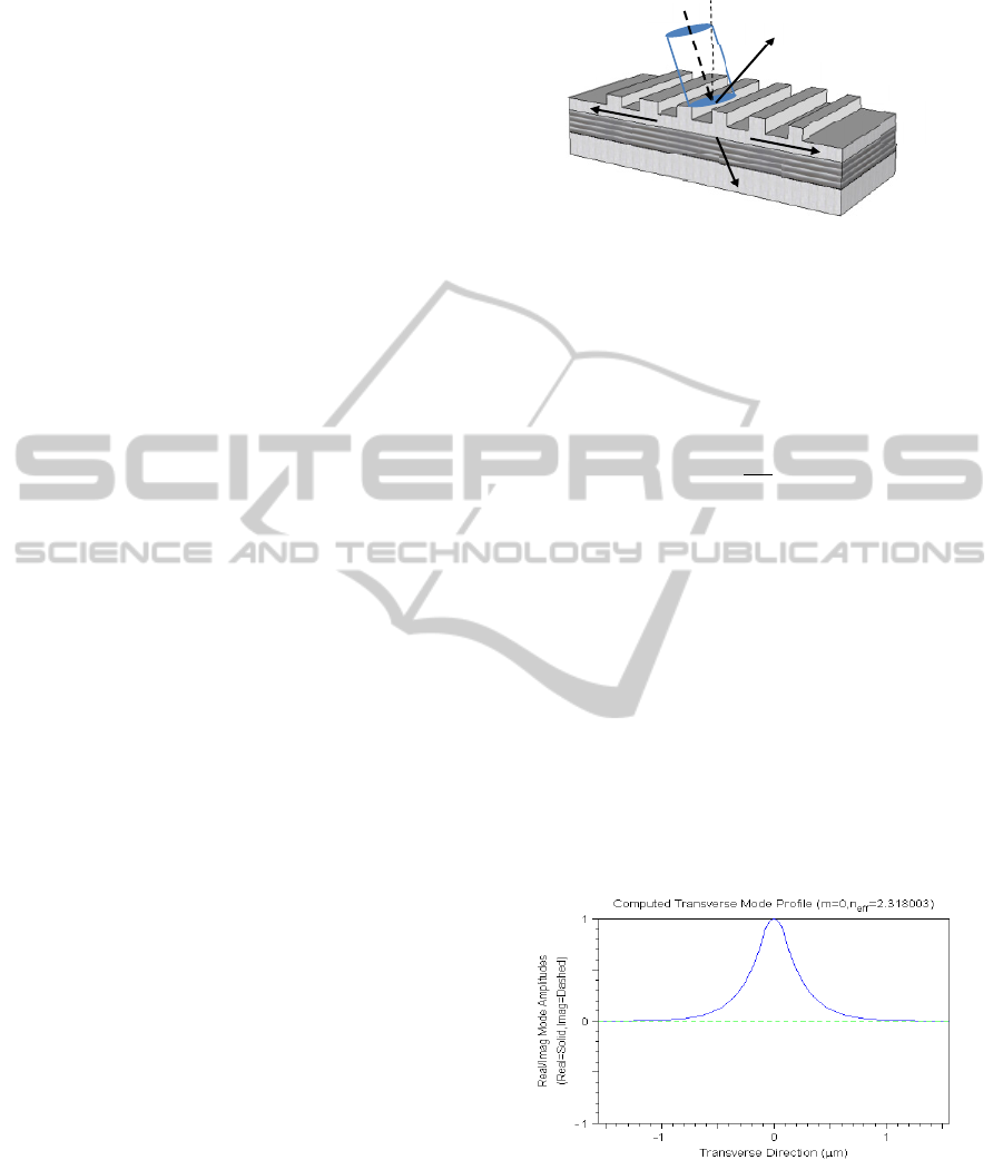
For an SOS planar waveguide structure, we can
obtain the effective refractive index (ERI) of the TE
mode n
eff
=2.318, we use Rsoft to compute n
eff
=2.318
when the thickness of the waveguide H is 220nm
(The limited thickness of TE
0
mode) λ =2.7μm as
shown in Fig.2.
Figure 2: The profile of waveguide mode.
Next, according to the phase match condition
between the gratings and the waveguide mode:
T
n
n
∙sinθ
mλ
m0, 1, 2⋯
(3)
Where n
clad
=1 (air) and the grating period T is equal
Si
Sapphi
Si
P
i
P
re
P
co
P
t
P
u
PHOTOPTICS2015-InternationalConferenceonPhotonics,OpticsandLaserTechnology
74
to 1.2603μm. In addition, the fill factor of grating f
which defined as the ratio of pillar width to grating
period is equal to 0.4. We can control the width of
each pillar to obtain the desired refractive index
distribution. With the calculations given above,
finally, all the parameters required for constructing a
subwavelength grating coupler based on SOS is
listed in Table.1.
Table.1: Design parameters of grating coupler (Unit:
Micrometers).
Parameters λ T h H W f θ
Value
2.
7
1.260
3
0.1
2
0.22 0.88
0.
4
10
º
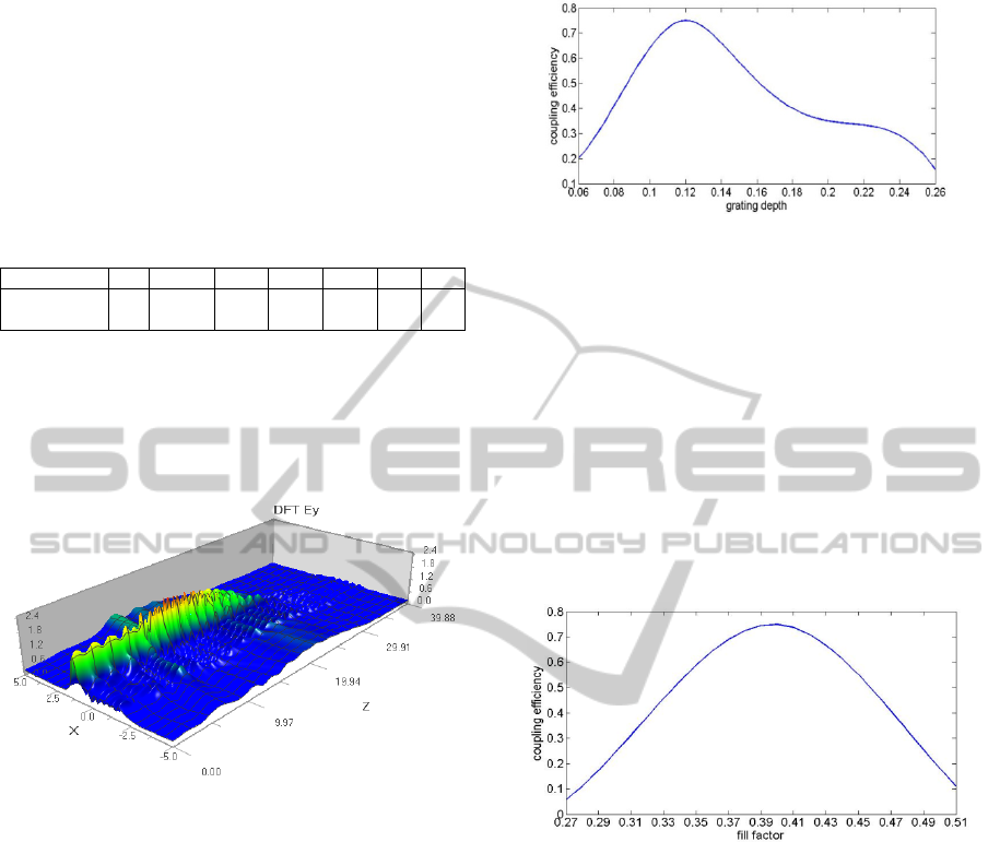
Simultaneously, the finite-difference time-domain
method, a powerful and accurate method for a finite-
size structure, is chosen to simulate and design this
device. For a 2.7μm wavelength, the coupling
efficiency is about 75% when we consider the TE.
The Ey component of optical filed is given in Fig. 3.
Figure 3: Distribution of optical field.
According to above theoretical analysis, we take
these parameters given in Table 1 as a starting point
to simulate and evaluate the performance of the
grating coupler described above. We will look at the
sensitivity of the grating couplers to variations in the
grating parameters. We introduce errors on the etch
depth, filling factor and grating width (period
tolerance).
In fabrication, considering requirements of
production process, the grating depth is hard to
control because electron beam density which is hard
to control current on the accuracy of the etching
depth. We will evaluate the influence of fabrication
error to the coupling efficiency. The resulting
coupling efficiency as a function of etching depth is
shown in Fig. 4.
It shows a maximum coupling efficiency around
75% (grating depth h=0.12μm) and a 1 dB depth
bandwidth of 50 nm (from 0.1μm to 0.15μm). When
the grating height is larger than 0.26μm or lower
than 0.06μm, the mismatch of mode profile between
Figure 4: Coupling efficiency as a function of grating
depth with λ=2.7μm, T=1.2603μm, f=0.4, θ=10º.
grating field and fiber will be large. Consequently, if
the grating is etched too deep or too shallow the
wavelength is obviously shifted to longer or shorter
wavelengths (not shown in Fig.4), and the second
order reflection is also increased. So the coupling
efficiencies are significantly low.
Fig.5 shows the effect of a different filling factor.
It shows a maximum coupling efficiency around
75% with grating depth f=0.4μm.Changing it from
0.4 to 0.35 or 0.45 has only a small effect on the
coupling efficiency curves, in which the coupling
efficiency is larger than 60%.
Figure 5: Coupling efficiency as a function of fill factor
with λ=2.7μm, T=1.2603μm, h=0.12μm, θ=10º.
Fig.6 shows the coupling efficiency as a function
of angle. The θ=10º curve has a maximum for
λ=2.7μm. The case of vertical coupling (θ=0º) is
very interesting from a practical point of view.
However, as above mentioned, in such case, the
second order diffraction is reflecting back into the
waveguide, which results in the coupling efficiency
obviously degenerated.
The effect of random errors on the groove widths
is shown in Fig.7. The coupling efficiency gets its
maximum value when the grating period error is 0
(T=1.2603μm). The errors have a normal (Gaussian)
distribution with half width 40nm (from -20nm to
20nm). Compared to the perfect structure, the
coupling efficiency is obviously reduced to the half
of the maximum.
HighPerformanceSilicon-on-SapphireSubwavelengthGratingCouplerfor2.7μmWavelength
75
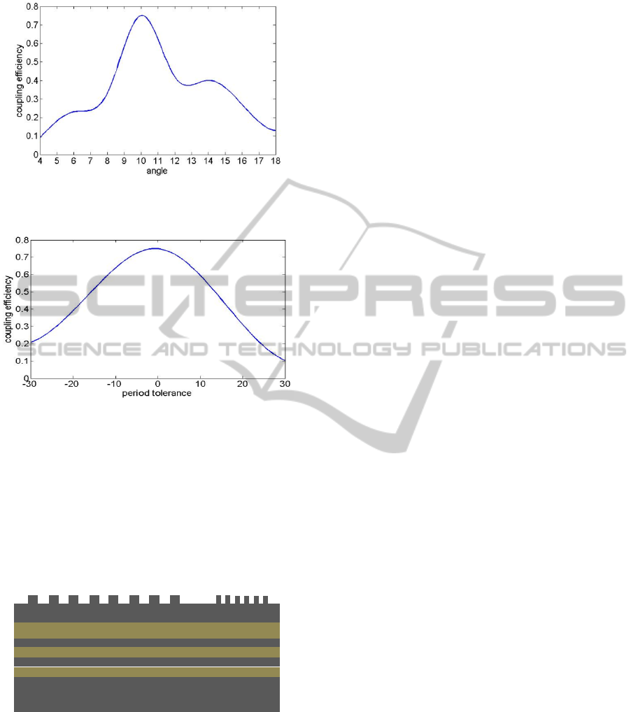
Figure 6: Coupling efficiency as a function of incidence
angle with λ=2.7μm, T=1.2603μm, h=0.12μm, f=0.4.
Figure 7: Influence of period tolerance on coupling
efficiency with λ=2.7μm, h=0.12μm, f=0.4, θ=10º.
In real fabricated structures these errors on the
different parameters are present all at the same time.
In the worst case scenario everything adds up, but it
is also possible that one error cancels the other. We
can conclude that the tolerances to fabrication errors
are very tight, but achievable. The high accuracy
needed is typical for all nanophotonic structures.
Figure 8: Optimized grating coupler using reflector grating
and Bragg reflection layers.
As above discussed, at the coupler grating, part of
the light is reflected P
re
, part is coupled out P
co
, part
is transmitted P
tr
and the rest is leaked down to
substrate P
un
. In order to improve the coupling
efficiency, one way is to add a second grating with
the same etch depth as the coupler grating, which
acts as a reflector behind the coupler grating as
shown in Fig.8. If the structure is properly designed
which the direct reflection at the coupler grating and
the reflection from the reflector grating interfere
destructively, it is possible to reduce the reflection at
the coupler and couple all light out. Simultaneously,
a bottom reflector can further improve the coupling
efficiency to fiber. This bottom reflector can be a
multi-layer dielectric mirror or a metal mirror. We
have chosen for a Bragg reflection layers consisting
of Si/Sapphire pairs. The thickness of each layer
t=λ/4n must be well controlled to obtain a high
reflectivity. n is the refractive index of the layer of
silicon and sapphire. Thanks to the high refractive
index contrast, only a few pairs are needed and the
reflection is broadband. Depend on above optimized
methods, the coupling efficiency beyond 80% can be
realized for mid-infrared wavelength.
4 CONCLUSIONS
In this paper, we proposed a subwavelength grating
coupler with coupling efficiencies exceeding 75% at
a wavelength of 2.7μm with an 50nm depth
bandwidth of 1dB. The coupling efficiency can
reach up to about 80% if the optimized method is
adopted. The gratings open the path to silicon
photonic chips for the mid-infrared enabling new
nonlinear optical functions as well as new
spectroscopic lab on-a chip approaches. Experiments
are being carried out and results will be presented
soon.
ACKNOWLEDGEMENTS
This work was supported by the National Natural
Science Foundation of China (60907003), the
Foundation of NUDT (JC13-02-13), the Hunan
Provincial Natural Science Foundation of China
(13JJ3001), and Program for New Century Excellent
Talents in University (NCET-12-0142). The authors
gratefully acknowledge helpful discussions with
Prof. Zhiping Zhou.
REFERENCES
B. E. A. Saleh and M. C. Teich, Fundamentals of
Photonics (John Wiley & Sons, Inc., 2007), p.39.
Richard Soref, Mid-infrared photonics in silicon and
germanium, Nature Photonics, 4, 495-497, 2010.
Richard A Soref, Stephen J Emelett and Walter R
Buchuald, Silicon waveguided components for the
Coupling
g
ratin
g
reflec
tor grating
Bragg
reflector
layers
PHOTOPTICS2015-InternationalConferenceonPhotonics,OpticsandLaserTechnology
76

long-wave infrared region, Journal of Optics A: Pure
and Applied Optics, 8, 840-848, 2006.
L. Labadie, and O. Wallner, Mid-infrared guided optics: a
perspective for astronomical instruments, Opt. Express
17, 1947-1962, 2009.
H. B. Gray, Chemical Bonds: An Introduction to Atomic
and Molecular Structure (University Science Books),
1994.
G. C. Holst and S. W. McHugh, Review of thermal
imaging system performance, Proceedings of SPIE,
78-84, 1992.
Xiaoping Liu, Bark Kuyken, Gunther Roelkens, Roel
Baets, Richard M. Osgood Jr, Willian M.J.Green,
Bridging the mid-infrared-to-telecom gap with silicon
nanophotonic spectral translation, Nature Photonics,
23, 667-671, 2012.
Jalali, B. et al. Prospects for silicon mid-IR Raman lasers.
IEEE J. Sel. Top.Quantum Electron. 12, 1618–1627
(2006).
Willer, U., Saraji, M., Khorsandi, A., Geiser, P. & Schade,
W. Near- and mid-infrared laser monitoring of
industrial processes, environment and security
applications. Opt. Laser Eng. 44, 699–710 (2006).
Moore, D. S. Instrumentation for trace detection of high
explosives. Rev. Sci. Instrum. 75, 2499-2512 (2004).
Namjou, K., Roller, C. B. & McCann, P. J. The
Breathmeter: a new laser device to analyze your
health. IEEE Circ. Dev. Magazine 22-28 (2006).
Capasso, F. et al. Quantum cascade lasers: ultrahigh-speed
operation, optical wireless communication, narrow
linewidth, and far-infrared emission. IEEE J. Quantum
Electron. 38, 511-532 (2002).
R. Soref, Towards silicon-based longwave integrated
optoelectronics (LIO), SPIE Proc. 6898, 689809,
689809-13 (2008).
G. Z. Mashanovich, M. M. Milošević, M. Nedeljkovic, N.
Owens, B. Xiong, E. J. Teo, and Y. Hu, Low loss
silicon waveguides for the mid-infrared, Opt. Express
19(8), 7112-7119 (2011).
M. M. Milošević, P. S. Matavulj, P. Y. Yang, A. Bagolini,
and G. Z. Mashanovich, Rib waveguides for
midinfrared silicon photonics, J. Opt. Soc. Am. B
26(9), 1760-1766 (2009).
T. Baehr-Jones, A. Spott, R. Ilic, A. Spott, B. Penkov, W.
Asher, and M. Hochberg, Silicon-on-sapphire
integrated waveguides for the mid-infrared, Opt.
Express 18(12), 12127-12135 (2010).
A. Spott, Y. Liu, T. Baehr-Jones, R. Ilic, and M.
Hochberg, Silicon waveguides and ring resonators at
5.5 μm, Appl. Phys. Lett. 97(21), 213501 (2010).
F. Li, S. D. Jackson, C. Grillet, E. Magi, D. Hudson, S. J.
Madden, Y. Moghe, C. O’Brien, A. Read, S. G.
Duvall, P. Atanackovic, B. J. Eggleton, and D. J.
Moss, Low propagation loss silicon-on-sapphire
waveguides for the mid-infrared, Opt. Express 19(16),
15212-15220 (2011).
Yang Liu, Alexander Spott, Tom Baehr-Jones, Rob Ilic,
Michael Hochberg, Silicon waveguides and ring
resonators at 5.5μm, Group Ⅳ Photonics(GFP), 2010
7
th
IEEE International Conference.
Mackenzie A. Van Camp, Solomon Assefa, Douglas M.
Gill, Tymon Barwicz, Steven M. Shank, Philip M.
Rice, Teya Topuria, and William M. J. Green1,
Demonstration of electrooptic modulation at 2165nm
using a silicon Mach-Zehnder interferometer, Optics
Express, 20(27), 28009-28016, 2012.
M. Muneeb, X. Chen, P. Verheyen, G. Lepage, S. Pathak,
E. Ryckeboer, A. Malik, B. Kuyken, M. Nedeljkovic,
J. Van Campenhout, G. Z. Mashanovich, and G.
Roelkens, Demonstration of Silicon-on-insulator
midinfrared spectrometers operating at 3.8μm, Optics
Express, 21(10), 11659-11669, 2013.
B. Kuyken, N. Hattasan, D. Vermeulen, S. Selvaraja, W.
Bogaerts, W. M. J. Green, R. Baets, G. Roelkens,
Highly Efficient Broadband Silicon-on-Insulator
Grating Couplers for the Short Wave Infrared
Wavelength Range,
OSA/ANIC/IPR/Sensors/SL/SOF/SPPCom/2011
Nannicha Hattasan, Bart Kuyken, Francois Leo, Eva M. P.
Ryckeboer, Diedrik Vermeulen, and Gunther
Roelkens, High-Efficiency SOI Fiber-to-Chip Grating
Couplers and Low-Loss Waveguides for the Short-
Wave Infrared, IEEE Photonics Technology Letters,
24(17), 1536-1538, 2012.
Zhenzhou Cheng, Xia Chen, C. Y. Wong, Ke Xu, Christy
K. Y. Fung, Y. M. Chen, Hon Ki Tsang, Mid-Infrared
Grating Couplers for Silicon-on-Sapphire
Waveguides, IEEE Photonics Journal, 4(1), 104-113,
2012.
Ananth Z. Subramanian, Shankar Selvaraja, Peter
Verheyen, Ashim Dhakal, Katarzyna Komorowska,
and Roel Baets, Near-Infrared Grating Couplers for
Silicon Nitride Photonic Wires, IEEE Photonics
Technology Letters, 24(19), 1700-1703, 2012.
Junbo Yang, Zhiping Zhou, XinJun Wang, Danhua Wu,
Huaxiang Yi, JianKun Yang, and Wei Zhou, Compact
double-layer subwavelength binary blazed grating 1×4
splitter based on silicon-on-insulator, Optics Letters,
36(6), 837-839, 2011.
Junbo Yang, Zhiping Zhou, Honghui Jia, Xueao Zhang,
and ShiQiao Qin, High-performance and compact
binary blazed grating coupler based on an asymmetric
subgrating structure and vertical coupling, Optics
Letters, 36(14), 2614-2616, 2012.
Dirk Taillaert, Grating couplers as Interface between
Optical Fibres and Nanophotonic Waveguides, Gent
University, 2005.
HighPerformanceSilicon-on-SapphireSubwavelengthGratingCouplerfor2.7μmWavelength
77
